Tutorial Series
tutorial series
Understanding SR Latches: Complete Guide to Set-Reset Latch, Gated & Clocked Versions

An SR latch is a basic memory element in digital electronics that stores binary data using Set and Reset inputs. This tutorial covers the SR latch truth table, the circuit diagram, and the working principle of basic, gated, and clocked SR latch variants.
Initially, after the introduction of transistors, engineers constructed simple latch circuits using transistors. After several stages of evolution, dedicated latches were built using logic gates like the NAND gate and NOR gate. These latches were used to store data, essentially binary data. In this article, we’ll briefly take a look at the SR Latch, along with its Gated SR Latch and Clocked SR Latch versions.
Quick Overview
Duration: 1-2 hours | Type: Digital Logic | Difficulty: Beginner
Technical Scope:
SR latch variants, truth tables, gate circuits
Use Cases:
Memory storage, control flags, data buffering, timing synchronisation
Table of Contents
What is a Latch?
The latch is just a simple bistable circuit and hence has two stable states: set (logic 1) and reset (logic 0). It is a digital circuit that stores one bit of information and retains that output until input variations change it. On the other hand, compared to flip-flops, latches are asynchronous sequential circuits and do not operate with the help of a clock signal. So, output changes occur immediately after the input changes when the latch is enabled.
Key Features of Latches
- Memory unit: Storing one data-bit as long as there is power.
- Asynchronous: There is no clock input; state changes directly with the input.
- Constructed from logic gates: Usually, the gates used will be NAND, NOR, AND, OR, and NOT.
- Basic building blocks of digital systems: They find use in data storage, control circuits, and sequential logic designs.
- Outputs: As the inputs change, outputs keep reflecting that change if it is enabled; else, they hold the stored value.
Types of latches
The primary types of latches that are used in digital circuits and systems
∗ SR Latch
∗ JK Latch
∗ D Latch
∗ T Latch
Let us now discuss the SR Latch in detail.
What is an SR Latch?- Complete Definition
The SR Latch, also known as the Set-Reset Latch, is a fundamental digital memory circuit that stores one bit of binary data using two inputs, namely Set (S) and Reset (R). When Set is activated, the latch outputs '1' (HIGH), and when Reset is activated, it outputs '0' (LOW). The stored value remains stable even after inputs are removed, making it a basic memory element. This latch can be built using either NOR or NAND gates, with the key difference being that NAND implementation uses inverted (active LOW) inputs compared to NOR gates.
Note: If a latch circuit, such as an SR Latch, is edge-triggered using a clock pulse, it becomes a flip-flop. So, ideally, latches and flip-flops are two different things and should not be confused for the same. In our case, if the SR latch is given a clock pulse, it becomes a clocked SR latch, which is also called an SR Flip-Flop.
If you are completely new to flip-flops and latches, check out our tutorial on the Basics of Flip-Flops in Digital Electronics.
More Digital Electronics Tutorials
Sequential Logic Circuits:
SR Latch Quick Reference Guide
| Parameter | Description | Function |
| Set (S) Input | Control input for setting output to HIGH | Forces Q = 1 when activated |
| Reset (R) Input | Control input for resetting output to LOW | Forces Q = 0 when activated |
| Q Output | Primary output representing stored bit | Shows current state (0 or 1) |
| Q̅ Output | Complementary output (inverted Q) | Always opposite of Q in stable states |
Key Elements of SR Latches
- Set (S) Input: Forces Q output to the HIGH state (logic 1)
- Reset (R) Input: Forces Q output to the LOW state (logic 0)
- Q Output: Primary output (representing stored bit)
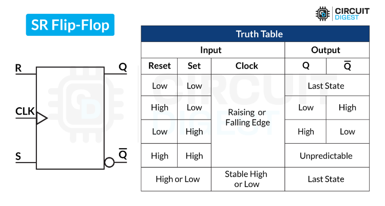
Sometimes you may also see a Q̅, which is nothing but an inverted output of Q. In the image below, you can see the symbol and a simple SR Latch truth table. From the table, you can notice that the logic is straightforward since it's a memory element.
SR Latch Truth Table - Complete Analysis
The SR latch truth table defines all possible input combinations and corresponding outputs. This table serves as the foundation for understanding SR latch behaviour in digital circuits.
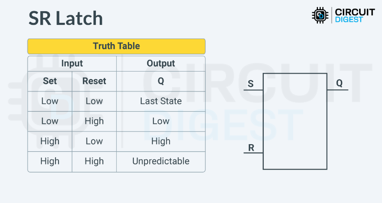
SR Latch Diagram States Explained
There are four possible logic states for this latch:
- When both inputs are LOW, the output remains unchanged. Initially, the output will be undefined (random), but after any other condition is applied, the “both LOW” state will retain the last output.
- When Set is LOW and Reset is HIGH, the output Q goes to the Reset state, which is LOW.
- When Set is HIGH and Reset is LOW, the output Q enters the Set state, which is HIGH.
- In the rare case where both Set and Reset are HIGH, the output Q becomes unstable due to the racing condition. Therefore, this state is considered invalid.
| Set (S) | Reset (R) | Q Output | Q̅ Output | State | Description |
| 0 | 0 | Qprevious | Q̅previous | Hold/Memory | No change - maintains previous state |
| 0 | 1 | 0 | 1 | Reset | Output forced to LOW (0) |
| 1 | 0 | 1 | 0 | Set | Output forced to HIGH (1) |
| 1 | 1 | ? | ? | Invalid/Forbidden | Undefined state - avoid in design |

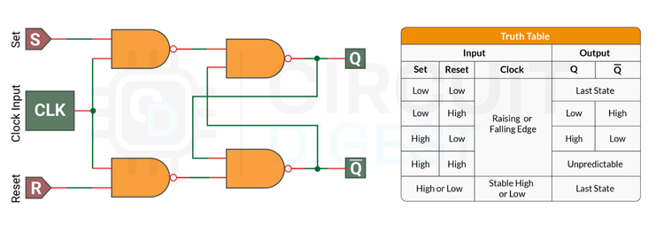
SR Latch Circuit Diagram - NAND and NOR Implementations
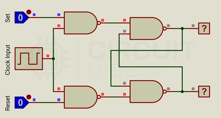
The SR latch circuit diagram can be implemented using either NAND gates or NOR gates, each with distinct characteristics and input polarities. Below, you can see a working simulation of a simple SR Latch made using NAND gates, built using Proteus. You can notice how the output values Q and Q̅ change based on the input values S and R.

Now, let’s take a look at the Gated and Clocked versions of the SR Latch.
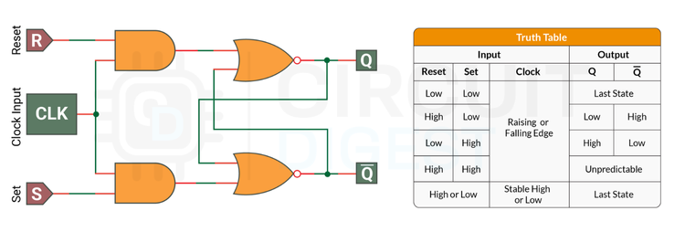
Gated SR Latch - Enhanced Control Mechanism
For the most part, the gates SR Latch is similar to the standard SR Latch. The only difference is the addition of one extra input, known as Enable. Below, you can see the Gated SR latch truth table and symbol for better understanding.

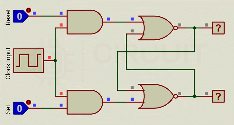
The Enable input allows us to enable or disable the latch, providing more control compared to the basic version. Below is a Gated SR Latch built using NAND logic gates in Proteus. This simulation will help you understand the concept clearly.
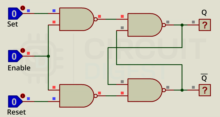
The logic here is generally the same as a standard SR Latch, with the only addition being the Enable input.
- If the Enable input is HIGH, the Gated SR Latch works as expected.
- If the Enable input is LOW, regardless of the S and R inputs, the output remains unchanged—in other words, the previous state is held.
Clocked SR Latch
The Clocked SR Latch, also known as the SR Flip-Flop, is very similar to the Gated SR Latch, except that the Enable input is replaced by a Clock input. Instead of a stable enable line, the output now depends on the rising or falling edge of the clock signal. This is called edge-triggered behaviour.
Below, you can see the symbol and the truth table for a better grasp of the concept.
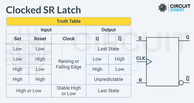
Clocked SR Latch Benefits
- Edge Triggered: Changes in state occur with the clock transition; the latch is insensitive to the input during any other time
- Noise-Immunity: Glitches get through only when the clock is not transitioning
- Synchronous Operation: Enables timing coordination in consecutive processes
- Timing Predictability: Sidesteps race hazards in systems with complex timing
So, this Clocked SR Latch is essentially an SR Flip-Flop. To learn more about this, you can check out the Flip-Flop in Digital Electronics article for additional information and practical demonstrations. You can also view the simulation result using Proteus in the simulation image below.
As mentioned earlier, the Clocked SR Latch is an edge-triggered device, which makes it more reliable for timed operations in sequential circuits. The working logic is slightly different from that of a regular latch circuit.
To keep it simple, here’s how it works:
- No Change (S = R = 0): The flip-flop retains its previous state.
- Set (S = 1, R = 0): Output Q becomes ‘1’ (Set).
- Reset (S = 0, R = 1): Output Q becomes ‘0’ (Reset).
- Invalid (S = R = 1): Both outputs (Q and Q̅) may become ‘1’, leading to instability. This condition is generally avoided in practical designs.
All these transitions happen only on the positive or negative clock edge, depending on the specific components used in the circuit.
SR Latch Applications in Modern Digital Systems
| Application Domain | Latch Type | Specific Use Cases | Key Benefits |
| Memory Systems | Clocked SR | Cache registers, buffer memory, register files | Fast access, reliable storage |
| Control Logic | Basic SR | State machines, flag registers, event detection | Simple implementation, low cost |
| Communication | Gated SR | UART buffers, protocol controllers, data latching | Controlled access, timing flexibility |
| Timing Circuits | Clocked SR | Clock dividers, frequency synthesis, timing generation | Precise timing, synchronization |
Frequently Asked Questions on SR Latch Table
⇥ 1. What is the difference between an SR latch and a D latch?
An SR latch works with two distinct inputs, Set and Reset, and careful activation of only one of the inputs is required to avoid race conditions. By contrast, a D latch has one data input; the complementing actions take place automatically, hence preventing invalid states and providing a simpler and more reliable operation for digital systems.
⇥ 2. What is invalid for the SR latch if S=1, R=1?
By establishing both inputs of the latch as HIGH and consequently trying to set a 1 at Q and reset a 0 at Q̅, creates an indeterminate state of either 0 or 1. This indeterminate state can initiate an oscillating output and/or lead to unpredictable or undefined behaviour of the circuit. More importantly, the race condition invalidates the fact that Q and Q̅ must be complementary values at any stable output state.
⇥ 3. What is the limiting factor of the SR latch propagation delay?
Propagation delay can restrict switching speed and timing margins. Propagation delay governs the maximum operating frequency of sequential circuits and the setup and hold time, and gated SR latches based on NAND typically achieve about 2-5ns of propagation delay, and NOR is assumed to be slower.
⇥ 4. What will happen to the output of the SR latch at power-on?
The latch will not have a defined output as it will be unpredictable due to component variation, as well as noise at startup. Most latch/systems would contain a power-on reset circuit to force a specific initial state and would likely take advantage of RC networks or power-on reset integrated circuits for reliable startup at system power-on.
⇥ 5. How much power does an SR latch consume?
For CMOS implementations, static power consumption will be almost negligible, with the exception of leakage current; however, dynamic power will depend on switching frequency. At moderate switching speeds, it would be quite minute, about 0.1 - 1 mW. Generally, a NAND implementation will consume less power than the NOR counterparts for most logic families.
⇥ 6. How will temperature affect the SR latch's behaviour?
Increased temperature will increase propagation delays while also compromising noise margins. Commercial-rated devices will be operable within a temperature range of 0 °C - 70 °C, with the industrial counterparts rated -40 °C - 85 °C. Compensation circuits may thus be needed for some applications that require exactness.
⇥ 7. How fast can SR latches operate at?
Most modern CMOS implementations of the SR latch can operate at a frequency of a few GHz, limited by the propagation delay of the latch and parasitic capacitances that result from wiring in the implementation. The practical frequency of operation will depend on what logic family the latch is in: TTL (50 - 100 MHz), CMOS (500 MHz - 2 GHz), and newer processes have demonstrated even greater speeds.
Conclusion
This tutorial covered the fundamental working principle, truth table, and circuit diagrams of basic SR latch, gated SR latch, and clocked SR latch implementations. Understanding these digital logic building blocks is essential for sequential circuit design and memory applications in electronics. If you have any questions, leave them in the comment sections at the bottom of this page, and we will be happy to answer them. You can also join our community or forums to start a discussion.
This tutorial was created by the Circuit Digest engineering team. Our experts focus on creating practical, hands-on tutorials that help makers and engineers master electronic circuit projects.
I hope you liked this article and learned something new from it. If you have any doubts, you can ask in the comments below or use our forum for a detailed discussion.
DIY Projects with SR Flip Flops
If you would like to learn more about SR Flip-Flops, these tutorials include helpful diagrams, truth tables, and logic circuits to guide you through the concepts.

Clocked SR Flip Flop: Complete Guide with Circuit, Truth Table, and Working
Learn how Clocked SR Flip-Flops work using NAND and NOR gates. Includes truth tables, logic diagrams, and real-world timing applications.

SR Flip-Flop with NAND Gates: Circuit, Truth Table and Working
Learn how to build an SR Flip-Flop circuit using NAND gates. Understand the logic, truth table, working principle, and output behaviour with a complete circuit diagram and explanation

What is Switch Bouncing and How to Prevent It Using a Debounce Circuit
Learn how switch bouncing can affect SR Flip-Flop circuits and how to prevent false triggering using debounce techniques like RC filters and Schmitt triggers in digital logic systems.
Add New Comment
Clocked SR Flip Flop: Complete Guide with Circuit, Truth Table, and Working

The Clocked SR flip flop is one of the most fundamental sequential logic circuits in digital electronics. Unlike basic SR latches, a clocked SR flip flop circuit uses a clock signal to control when state changes occur, making it essential for synchronous digital systems. This comprehensive guide covers the clocked SR flip flop truth table, circuit diagrams using both NAND and NOR gates, working principles, and practical applications in modern electronics.
Whether you're learning about flip-flops or designing sequential circuits, or troubleshooting memory systems, understanding how a clocked SR flip flop works is crucial for mastering synchronous logic design. We'll explore both positive edge-triggered and level-triggered implementations, compare NAND vs NOR gate designs, and demonstrate real-world applications where precise timing control is essential.
What is a Clocked SR Flip Flop? (Clocked RS Flip Flop)
The Clocked SR flip flop, also called a Clocked RS flip flop or gated SR flip flop, is a synchronous sequential logic circuit that combines the functionality of a basic SR latch with clock-controlled timing. This clock input acts as the heartbeat of the circuit, ensuring that every change in the stored bits happens only during specific clock pulses, making synchronisation between multiple flip-flops much easier than using basic latches. To understand the complete landscape of sequential logic circuits, you can explore our comprehensive guide on Flip-Flop in Digital Electronics: Types, Truth Table, Logic Circuit, and Practical Demonstration.
The Clocked SR (Set-Reset) Flip-Flop or Clocked RS Flip-Flop is an upgraded version of the SR or RS latch, which adds clock synchronisation for better timing control in digital systems. The Clocked SR flip-flop has a total of three inputs:
Set (S)
Reset (R)
Clock (CLK)
Here, during the rising or falling edge of the clock pulse, the flip-flop responds, unlike a latch, which operates continuously.
In the truth table below, the output (i.e., stored data) changes only when an active clock signal is applied. Otherwise, even if S or R is active, the data remains unchanged. This clock-controlled behaviour makes it synchronous and much more reliable for sequential circuit applications.
Clocked SR Flip Flop Truth Table and Symbol
The clocked SR flip flop truth table is essential for understanding how this sequential circuit responds to different input combinations. Below is the complete Clocked SR flip flop diagram showing all possible states of Set (S), Reset (R), Clock (CLK), and the resulting outputs Q and Q̅.
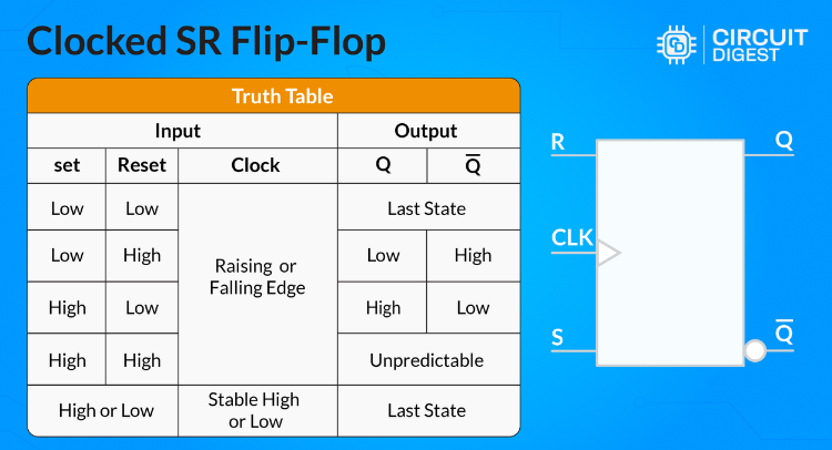
The truth table shows how the flip-flop reacts to different input combinations:
⇒ When the Clock is LOW, the values of S and R don’t matter — the output stays the same as before. No change happens until the clock goes HIGH.
⇒ When the Clock is HIGH, and both the Set and Reset are LOW, the output remains unchanged. It simply holds the previous state.
⇒ When Clock is HIGH, Set is HIGH and Reset is LOW, the output Q becomes HIGH, and Q̅ becomes LOW. This is the Set condition.
⇒ When Clock is HIGH, Set is LOW, and Reset is HIGH, the output Q becomes LOW, and Q̅ becomes HIGH. This is the Reset condition.
⇒ When the Clock is HIGH, and both the Set and Reset are HIGH, the output becomes invalid or unpredictable. This is a forbidden state and should be avoided.
Next, let's take a deeper look at how the Clocked SR (or RS) Flip-Flop works.
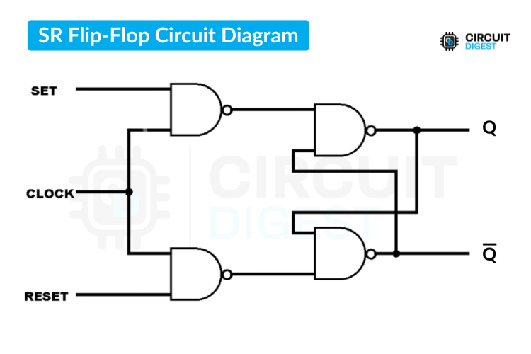
Clocked SR Flip Flop Using NAND Gate
The most common implementation uses NAND gates. For this, a clocked S-R flip-flop is designed by adding two NAND gates to a basic NOR gate flip-flop. The circuit diagram of the Clocked SR (or RS) Flip Flop that uses a NAND Gate is shown below.
The circuit typically consists of:
A basic SR latch made from NAND gates
Another set of NAND gates that act as clock-controlled switches, along with the S and R inputs
Working Operation in the Clocked SR Flip Flop Using NAND Gate
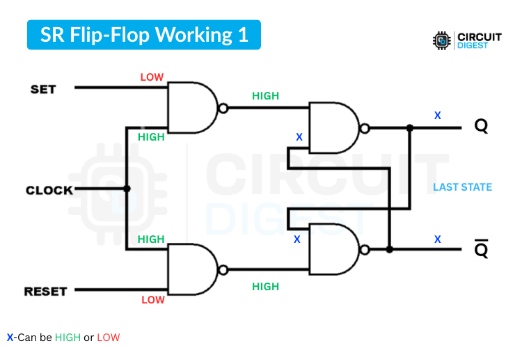
When the value of the clock pulse is '0', the outputs of both the AND gates will be low, effectively disabling the S and R inputs. This means the flip-flop will hold its previous state regardless of what happens at the S and R inputs.
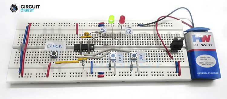
The SR flip-flop works based on basic logic gate combinations. If you follow the signal path through each gate, it’s easy to see how the outputs change. Below, you can see the simulation of the Clocked SR Flip-Flop using NAND gates made in Proteus.
When both Set and Reset are LOW, the output stays the same as before. It's like the flip-flop is remembering its last state. However, this can behave slightly differently in simulations versus real hardware, so keep that in mind.
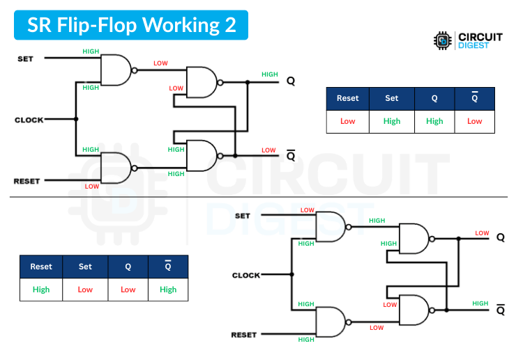
When Set is HIGH and Reset is LOW, the output Q becomes HIGH, and Q̅ becomes LOW. This is called the "Set" condition.
When Reset is HIGH and Set is LOW, the output Q goes LOW, and Q̅ becomes HIGH. This is the "Reset" condition.
When both Set and Reset are HIGH, this causes an invalid or unpredictable output. It creates a race condition, which can lead to instability, so it's something we should always avoid.
The key advantage of this design is timing control. The SR flip-flop can be used to synchronise data signals between two digital circuits, ensuring that they operate on the same clock cycle. This is useful in communication systems where data needs to be transmitted and received at specific times.
Clocked SR Flip Flop using NOR gate
The Clocked SR Flip-Flop using NOR gates employs NOR gates along with additional AND gates for clock control. In this design, a clocked S-R flip-flop is created by adding two AND gates to a basic NOR gate flip-flop. The circuit diagram of the Clocked SR (or RS) Flip Flop that uses a NOR Gate is shown below.
The circuit typically consists of:
Two AND gates that receive the S, R, and Clock inputs
A basic SR latch made from NOR gates
The AND gates act as clock-controlled switches
When the clock pulse goes HIGH (for a positive-edge-triggered flip-flop), the AND gates let the Set (S) and Reset (R) signals pass through to the SR latch inside. From there, the flip-flop behaves just like a regular SR latch:
If S is HIGH and R is LOW, the output Q becomes HIGH.
If S is LOW and R is HIGH, the output Q becomes LOW.
If both S and R are LOW, the output stays the same as before, and it holds the last state.
If both S and R are HIGH, the output becomes unpredictable. This is an invalid condition and should always be avoided.
The working operation of this Clocked SR Flip Flop using NOR Gate can be briefly observed in the GIF video below, which shows the simulation done using Proteus.
Key Advantages of SR Flip-Flops
The main advantage over basic SR latches is that a gated SR latch (or clocked SR latch) can only change its output state when there is an enabling signal along with valid inputs. This prevents unwanted state changes and eliminates timing issues common with asynchronous latches.
Most clocked SR flip-flops are positive edge-triggered, meaning they respond to the rising edge of the clock signal, though some designs may use negative edge-triggering or level-triggering depending on the application.
- Synchronous operations get rid of timing glitches.
- State change control rules out glitches and races.
- Memory function stores one-bit information.
- An accurate timing system is put in place with the clock edge trigger.
- Noise immunity helps to disable the false trigger.
Applications of SR Flip-Flops
Clocked SR Flip-Flops are widely used in digital systems that require synchronised operation, such as:
- Data synchronisation between different circuit blocks
- Memory registers in microprocessors and controllers
- State machines where timing control is critical
- Counter circuits and sequential logic systems
- Control systems that need precise timing coordination
Frequently Asked Questions on Clocked SR Flip Flop
⇥ 1. What is the difference between a clocked SR flip-flop and an SR latch?
A clocked SR flip flop has a clock signal that controls when state changes may occur, whereas an SR latch immediately responds to a change in input. The digital systems use a clock to synchronize events so that unwanted state transitions cannot occur.
⇥ 2. Why is the S=1, R=1 condition forbidden in a clocked SR flip-flop?
The set and reset are entered HIGH simultaneously, which establishes a condition wherein both outputs strive to become LOW, producing unpredictable consequences and possibly an oscillation that may damage the circuit.
⇥ 3. How is clock edge triggering performed with the clocked SR flip-flop?
With fall/rise clock edge triggering, the flip-flop or conditioning circuits respond during selected clock transitions. With this method, it is possible to allow one precise timing instance and speed execution of other actions so that there can be no more changes in state during a current clock pulse period.
⇥ 4. How do you prevent setup and hold time violations in a clocked SR flip-flop?
Your Set and Reset inputs should stabilise before the clock edge (setup time) and hold after the clock edge (hold time). Utilise your timing analysis, and if necessary, insert buffers.
⇥ 5. What is the propagation delay in a clocked SR flip-flop?
Propagation delay is the time from when the clock edge triggers to the time when the output will change. Generally, this takes 5-20 nanoseconds, depending on what your technology is. This will be factored into your maximum operating frequency and other timing calculations often required in digital systems.
⇥ 6. Can the clocked SR flip-flop operate without an external clock signal?
No, the clocked SR flip-flop needs an external clock signal to function properly. Without the clock signal, it acts as a basic latch with always sensitive inputs, effectively losing the advantages of synchronisation.
Exploring Other Flip-Flop Types
Now that you understand the SR flip-flop, you might want to explore other essential flip-flop types that build upon these concepts

T Flip-Flop: Circuit, Truth Table and Working
Learn how a T Flip-Flop works, along with its circuit, truth table, and timing diagram. This guide explains toggle flip-flop operation in digital electronics, comparing it with other types like JK and D flip-flops. Ideal for electronics students and circuit designers exploring sequential logic systems.

JK Flip-Flop: Circuit, Truth Table and Working
Learn how the JK Flip-Flop works with circuit diagrams, truth table, and timing explanation. Understand its toggling behavior and practical applications.

D Type Flip-Flop: Circuit, Truth Table and Working
Explore the working of D Flip-Flops with circuit diagrams, truth table, and timing details. Learn how data is stored and transferred in digital systems.
SR Flip-Flop with NAND Gates: Circuit, Truth Table and Working
Learn how to build an SR Flip-Flop circuit using NAND gates. Understand its working, truth table, and behavior for digital memory and control applications.
T Flip-Flop: Circuit, Truth Table and Working
Explore the T Flip-Flop circuit with working explanation, truth table, and timing diagram. Ideal for frequency division and toggle operations in digital circuits.
Add New Comment
What is Amplitude Modulation? Complete Guide with Formula, Circuit Diagram & Practical Demo

Amplitude modulation (AM) was first introduced to enable long-range wireless audio communication, representing a major advancement over wireless telegraphy using spark-gap transmitters. Understanding what is amplitude modulation and how it works is fundamental for electronics engineering students and professionals working with radio frequency circuits. This comprehensive guide covers amplitude modulation theory, circuit design, practical implementation, and real-world testing results with oscilloscope demonstrations.
Speaking about modulation, in simple terms, it's the method used to impose the message signal on a carrier signal, which is then transmitted by antenna or wire. And demodulation is practically the exact opposite, where the message signal is extracted from the carrier wave and used. In this article, we are going to learn about modulation and more about amplitude modulation with a practical circuit implementation.
Table of Contents
- Modulation and Its Types
- Amplitude Modulation Theory
- How Does Amplitude Modulation Work? Step-by-Step Process
- Amplitude Modulation Waveform
- Amplitude Modulation Advantages and Disadvantages
- Amplitude Modulation Practical Demonstration
- Amplitude Modulation Circuit Diagram
- Amplitude Modulation FAQ - Common Questions Answered
- DIY Projects on Wireless Audio Transmission
Modulation and Its Types
Modulation is the process of adding information, like sound or data, to a high-frequency signal called a carrier wave so it can travel long distances or be sent more efficiently through wires or the air. Even though modulation itself looks simple, there are three main methods of modulation. They are:
Amplitude Modulation
Frequency Modulation
Phase Modulation
Below you can see a simple comparison chart that explains the basic differences between each type of modulation technique:
And remember that there are still more types of modulation available, like Pulse Amplitude Modulation (PAM), Pulse Width Modulation (PWM), Pulse Position Modulation (PPM), Frequency Shift Keying (FSK), Phase Shift Keying (PSK), Quadrature Amplitude Modulation (QAM), and more, as technology is getting improved day by day.
Amplitude Modulation Theory
Amplitude Modulation (AM) is a method of sending information, like voice or music, by changing the strength (amplitude) of a high-frequency carrier wave based on the input signal. It allows us to transmit audio over long distances using radio waves and forms the foundation of AM radio broadcasting systems.
So, you need to understand the meaning of amplitude first to understand AM clearly.
Amplitude of a Signal
In simple terms, amplitude is how strong or intense a wave is. It's plotted on a graph with time on the x-axis and amplitude on the y-axis. It's how loud the sound wave is, think of it as more volume, more sound, more amplitude.

It's usually measured in volts (V) for electrical signals, decibels (dB) for sound, or other units depending on the context.
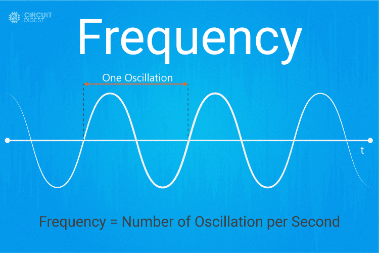
Frequency of a Signal
Frequency is the number of times a wave with the same pattern repeats itself in one second. It tells us how fast a wave is vibrating. For example, a frequency of 50 Hz means the wave cycles 50 times every second.
It's usually measured in Hertz (Hz). Now let's take a deeper look at amplitude modulation and understand how it works step by step.
How Does Amplitude Modulation Work? Step-by-Step Process
Understanding how amplitude modulation works step by step is crucial for electronics engineers and students. The AM process involves three main stages: carrier wave generation, message signal preparation, and the modulation process itself. Here's how amplitude modulation works in practice:
Carrier Wave Generation: A high-frequency sine wave (typically 535 kHz to 1700 kHz for AM radio) is generated using an oscillator circuit like the ICL8038 or similar function generator.
Message Signal Input: The audio or data signal that contains the information to be transmitted is prepared and amplified to appropriate levels.
Modulation Process: The amplitude of the carrier wave is varied according to the instantaneous amplitude of the message signal using a modulator circuit.
Signal Combination: The modulated signal combines both the carrier frequency and the message information in a single waveform.
Transmission: The modulated signal is amplified and transmitted through an antenna for long-distance communication.
This step-by-step amplitude modulation process ensures that low-frequency audio signals can be transmitted over long distances by riding on high-frequency carrier waves.
Amplitude Modulation Waveform
Below, you can see the image that clearly illustrates the modulated wave along with the carrier wave and the message signal, showing how the AM waveform is formed.
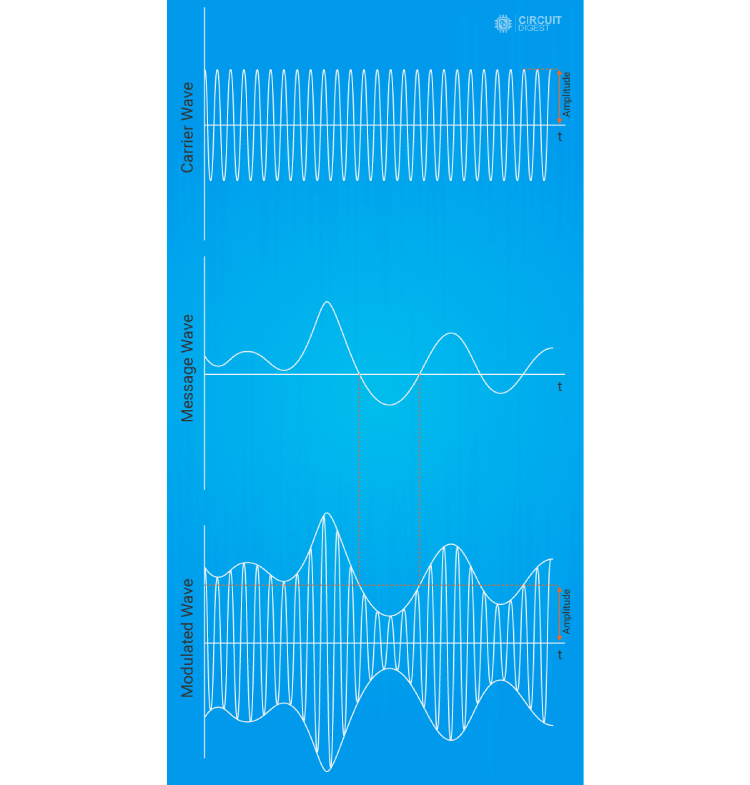
The first wave shown is the carrier signal.
In the case of AM radio, the carrier signal will be a medium-frequency wave, typically from 535 kHz to 1700 kHz. This carrier signal is generally a pure sine wave, generated using a dedicated oscillator circuit.
The next wave is a simple example message signal for demonstration. In this message wave, there is no specific frequency or amplitude. It's all random, which is how a real message would be. But the only thing is that the frequency of the message signal will be lesser than the carrier wave frequency.
Now, in the third modulated signal, you can see that the amplitude of the upper side of the carrier signal looks exactly like the message signal. This is how amplitude modulation works. In general, this effect can be achieved easily using a single transistor, where the carrier wave is amplified with respect to the input message signal, just like that.
AM Signal Equation Explained
The amplitude modulation formula derivation starts with understanding how the message signal modifies the carrier amplitude. This AM signal equation explained below shows the mathematical relationship between carrier, message, and modulated signals:
s(t)=[Ac+m(t)]cos(2πfct)
Here,
s(t): Refers to the modulated signal as a function of time. Sometimes this modulated signal is also represented as v(t), which is more specific as a voltage signal and is mostly used in circuit analysis. In general, this modulated signal can be represented as s(t).
Ac: Refers to the amplitude of the carrier wave that is used.
fc: Refers to the frequency of the carrier wave.
m(t): Refers to the modulating message signal as a function of time.
Amplitude Modulation Formula Derivation Explained
To understand the amplitude modulation formula derivation, let's break down each component. The modulation index (m) is a crucial parameter that determines the depth of modulation and can be calculated as m = Am/Ac, where Am is the amplitude of the message signal and Ac is the carrier amplitude. For proper AM transmission without distortion, the modulation index should not exceed 1 (100% modulation).
The complete AM formula derivation shows that the modulated signal contains the original carrier frequency plus upper and lower sidebands that carry the actual information. This mathematical foundation is essential for understanding how AM modulator circuits work in practice.
Now let's get into a practical demonstration for clear understanding.
Amplitude Modulation Advantages and Disadvantages
When designing AM circuits, it's important to understand the advantages and disadvantages of amplitude modulation compared to other modulation techniques like FM and digital modulation:
Advantages of Amplitude Modulation:
Simple circuit design and low-cost implementation compared to FM circuits
Easy demodulation using simple diode detectors without complex circuitry
Good long-range transmission capabilities, especially during nighttime propagation
Minimal bandwidth requirements (bandwidth = 2 × message signal bandwidth)
Mature technology with well-established manufacturing processes
Compatible with low-cost receivers, making it accessible worldwide
Disadvantages of Amplitude Modulation:
Poor noise immunity compared to FM and digital modulation techniques
Lower power efficiency due to continuous carrier transmission (only 33% efficiency at 100% modulation)
Susceptible to atmospheric interference and electrical noise
Limited audio quality compared to modern FM and digital broadcasting
Fading effects during long-distance transmission can cause signal degradation
Amplitude Modulation Practical Demonstration
To demonstrate amplitude modulation, we came up with a simple circuit using minimal components that you can try yourself.
Components Required
To keep this demonstration simple, I will be using commonly available components that are easy to find. Here's the complete list for building your own AM modulator circuit:
Below are the key components involved in the modulation process.
BC547 - 1 (Common NPN Transistor)
7805 - 1 (5v Voltage Regulator)
Resistor - 470Ω - 3
Resistor - 100Ω - 1
Resistor 1KΩ - 1
Capacitor - 470nF-2
Capacitor - 10pF-1
Modules
These modules are added only to reduce the complexity of the circuit used for testing amplitude modulation. With these, two major complexities solved, the circuit for generating the carrier signal and the circuit for the microphone setup for the message signal.
ICL8083 - 1(For Carrier Signal Generation)
Bluetooth Audio Receiver - 1(For message signal input)
Amplitude Modulation Circuit Diagram
Before getting into the actual circuit diagram, let's understand the basic working behind the circuit diagram.
How to Build AM Modulator Circuit - Step by Step Guide
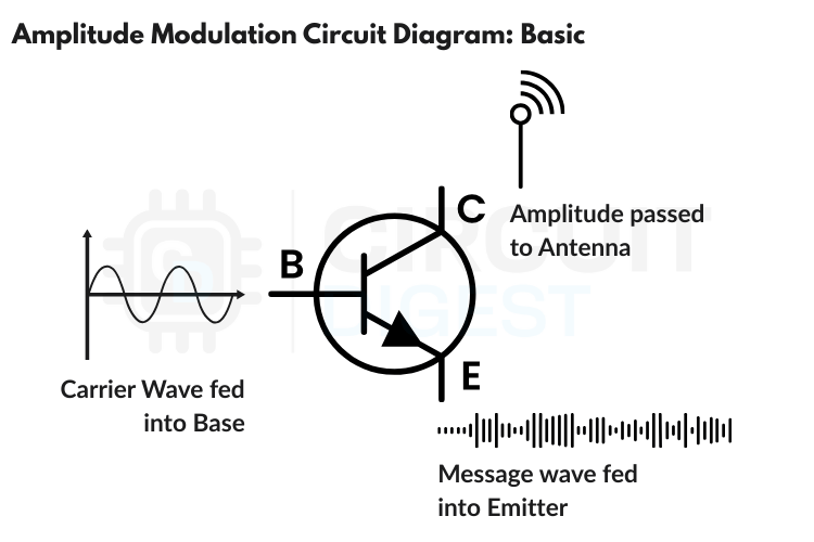
The image below shows the basic concept behind amplitude modulation. Depending on the real-time application, there might be some upgrades, but the core concept remains the same.
This amplitude modulation circuit design using BC547 transistor is perfect for students learning how to build AM modulator circuits. The circuit demonstrates the fundamental principle of AM generation and can be easily replicated on a breadboard. For beginners wondering how to make amplitude modulation circuit at home, this design uses commonly available components and provides clear, observable results on an oscilloscope.
The transistor acts like a variable amplifier controlled by two signals:
RF (Radio Frequency) input that comes from the oscillator (the medium-frequency carrier wave), and
Audio input that comes from a music source (like a computer, phone, or microphone).
The transistor works like an automatic volume control. As the audio signal gets louder, it makes the radio signal stronger. When the audio gets quieter, it makes the radio signal weaker.
This creates a modified radio signal where:
The frequency stays the same (like the radio station's channel),
The strength (amplitude) changes to match the message audio.
Any AM radio can detect these strength changes and convert them back into sound, simply by reversing the process.
Schematics of the AM Modulator
As you already know, to reduce the complexity, we are using separate modules for generating the carrier wave and feeding the message signal.
To clearly understand how the carrier wave is generated using the ICL8038, I recommend visiting the article: "How to Configure the ICL8038 to Generate a Sine Wave?" In our case, the only thing you need to know is that we power the ICL8038 module with 12V to ensure a higher frequency output.

In the above circuit diagram, you can clearly see the complete layout.
The generated sine wave (carrier wave) is fed into the base of the transistor with the help of a coupling capacitor. The base is also stabilized using two biasing resistors of 470Ω each.
For the message signal, we're using a simple, inexpensive Bluetooth audio receiver, the same module used in the project , Simple DIY Wireless Bluetooth Speakers using Audio Amplifier.
The audio output of the Bluetooth module is connected to the emitter of the transistor using a coupling capacitor. And that's it, most of the circuit is ready!
In practical AM transmitter circuits, a dedicated RF amplifier stage is added before the antenna. In simpler circuits, a small capacitor is used to block DC while allowing RF to pass, and sometimes a basic LC filter is used to reduce harmonics.
But in our case, since we're not using an AM receiver to test this setup and only want to observe it using an oscilloscope, we've added just a DC blocking capacitor at the output.
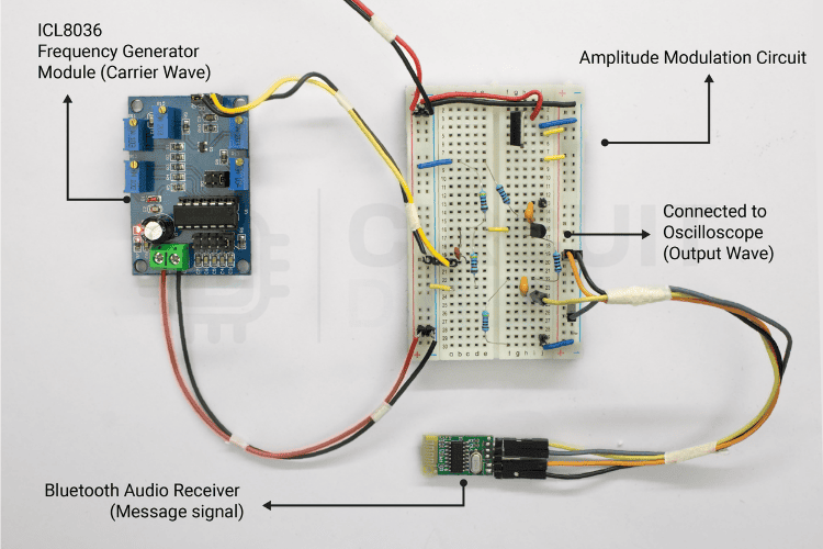
Powering the circuit is also important. I used a regulated power supply (RPS) to provide 12V to the entire circuit. This 12V powers both the ICL8038 module and the modulator transistor. A 7805 voltage regulator is used to provide 5V to the Bluetooth module.
Testing Our AM Modulator Setup
Testing was simple. I used my smartphone to send the message signal and an oscilloscope to verify the output and observe the amplitude modulation waveform in real time.
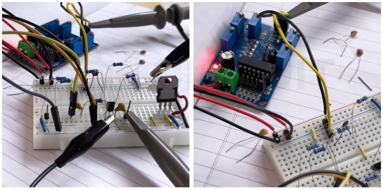
First, after connecting the breadboard to a 12V power supply, I checked for any faults.
I recommend you do the same, if the transistor is inserted with the wrong polarity, it may heat up quickly and its hFE (gain factor) could degrade over time.
Next, it was time to tune the carrier frequency on the ICL8038 module. I have set it to 380 kHz just as an example, you can set any high frequency of your choice for your AM modulator testing.
For precision, I used an oscilloscope to tune and verify the frequency.
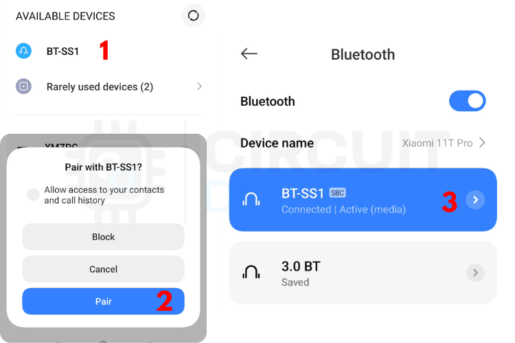
I opened the Bluetooth settings on my smartphone and paired it with the Bluetooth audio receiver. If you don't have a Bluetooth module, you can also use a simple AUX cable from your phone to extract the audio signal for amplitude modulation testing.
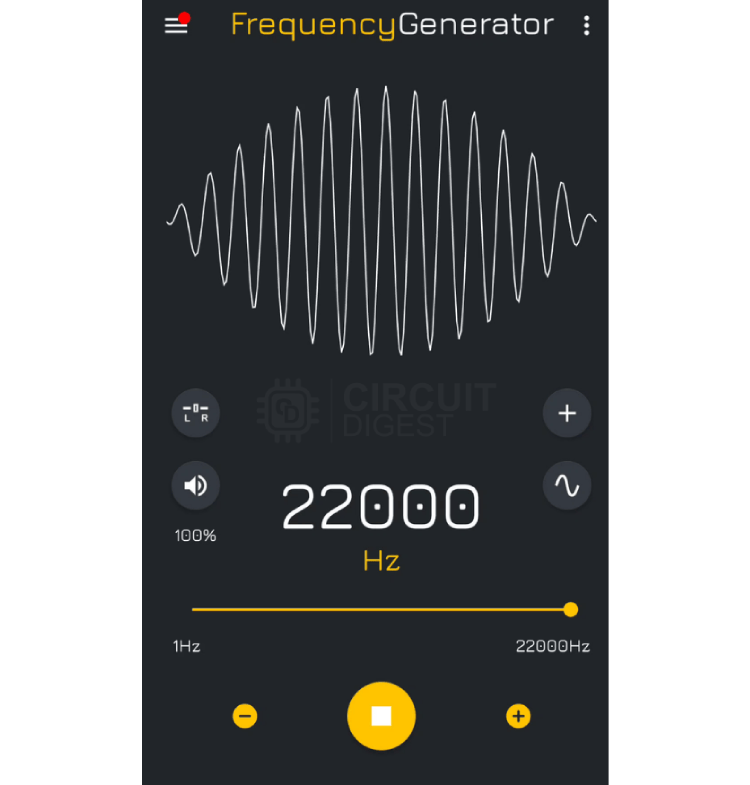
Next, I opened a frequency generator app. You can use any app for sound or even music. But for clearer oscilloscope visuals and better amplitude modulation demonstration, I chose to generate a stationary sine wave.
Using the app, I generated a 22 kHz sine wave and connected the second probe of the oscilloscope to the circuit's output to observe the amplitude modulation results.
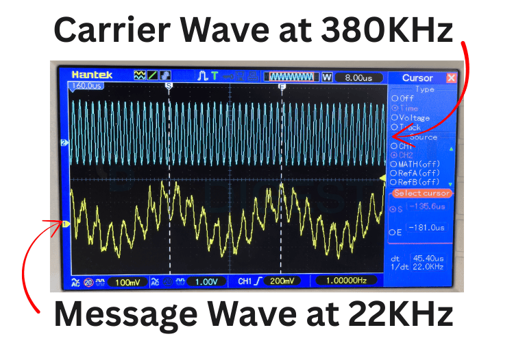
The oscilloscope display shows two important signals: the white trace (top) displays our 380 kHz carrier wave output from the AM modulator, while the yellow trace (bottom) shows the 22 kHz message signal from our phone app. The key observation is how the amplitude of the carrier wave (white) varies up and down following the exact pattern of the message signal (yellow), this varying envelope is amplitude modulation in action.
Notice how when the yellow message wave reaches its peak, the carrier amplitude becomes maximum, and when the message wave hits its lowest point, the carrier amplitude becomes minimum. This direct relationship proves our circuit is successfully impressing the audio information onto the high-frequency carrier wave. Please note that in the image above the carrier wave appears "inverted" due to our NPN transistor configuration, but this doesn't affect functionality.
This oscilloscope result confirms perfect amplitude modulation, the carrier frequency stays constant at 380 kHz while its amplitude varies according to our 22 kHz message signal. Any AM radio tuned to 380 kHz would detect these amplitude changes and convert them back into the original 22 kHz audio tone, demonstrating how AM radio communication works in practice.
Amplitude Modulation Circuit Troubleshooting Guide
When building your own AM modulator circuit, you might encounter some common issues. Here's a comprehensive troubleshooting guide for amplitude modulation circuits that will help you identify and fix problems quickly:
Common AM Circuit Problems and Solutions:
No Output Signal: Check power supply connections (ensure 12V is reaching ICL8038 and transistor), verify transistor orientation (BC547 pinout: CBE from left), and confirm all ground connections are secure
Distorted Modulation: Reduce message signal amplitude using volume control, check biasing resistor values (470Ω resistors), and ensure carrier frequency is much higher than audio frequency
Weak Carrier Signal: Verify ICL8038 module connections and power supply, adjust frequency control potentiometer, and check coupling capacitor connections
Overmodulation (Signal Clipping): Reduce audio input level from smartphone or Bluetooth module, check transistor biasing point, and ensure adequate power supply current
Poor Modulation Depth: Increase audio signal amplitude carefully, verify emitter coupling capacitor (470nF), and check transistor gain (hFE should be >100)
Oscilloscope Shows No Modulation: Ensure both carrier and audio signals are present, check probe ground connections, and verify oscilloscope trigger settings
AM Circuit Testing Tips:
Always test carrier signal first before adding audio input
Use low audio frequencies (100Hz-1kHz) for initial testing
Monitor transistor temperature - it shouldn't get hot during normal operation
Start with low modulation depth and gradually increase
Amplitude Modulation FAQ - Common Questions Answered
What is the difference between AM and FM modulation?
The main difference between AM and FM modulation is that AM (Amplitude Modulation) varies the amplitude of the carrier wave while keeping frequency constant, whereas FM (Frequency Modulation) varies the frequency while keeping amplitude constant. AM has simpler circuits and better long-range propagation but lower noise immunity compared to FM. AM radio operates in 535-1700 kHz band while FM radio uses 88-108 MHz band.
Why is amplitude modulation still used today?
Amplitude modulation is still used in AM radio broadcasting, aviation communications, and amateur radio because of its simplicity, excellent long-range propagation characteristics (especially at night), and the low cost of AM receivers. Many developing countries rely on AM radio for information dissemination due to its cost-effectiveness and simple receiver design.
What components are needed for a basic AM transmitter?
A basic AM transmitter requires an oscillator for carrier generation (like ICL8038), a modulator circuit (often using a transistor like BC547), an audio amplifier for the message signal, coupling capacitors, biasing resistors, and an RF amplifier stage before the antenna. Our demonstration uses BC547 transistor, ICL8038 module, resistors, capacitors, and basic passive components for a complete working AM modulator.
How do you calculate modulation index in amplitude modulation?
The modulation index (m) in amplitude modulation is calculated as m = Am/Ac, where Am is the amplitude of the message signal and Ac is the carrier signal amplitude. For undistorted transmission, the modulation index should not exceed 1 (100% modulation). Values above 1 cause overmodulation and signal distortion.
What is the bandwidth of an AM signal?
The bandwidth of an AM signal is twice the highest frequency of the modulating message signal. For example, if the audio signal has a maximum frequency of 5 kHz, the AM signal bandwidth will be 10 kHz. This is much narrower than FM signals, making AM more spectrum-efficient.
Can I build an AM radio transmitter legally?
Building AM transmitters for educational purposes is generally allowed, but transmitting signals over certain power levels requires licensing from your country's telecommunications authority. Always check local regulations before building and operating any radio transmitter. Low-power educational demonstrations are typically permitted.
DIY Projects on Wireless Audio Transmission
Discover practical implementations of wireless audio communication with these projects, ranging from ESP32-based internet radio to advanced wireless audio transfer using nRF24L01 modules, Li-Fi, and even LEDs. These amplitude modulation related projects will help you understand various wireless communication techniques.

Wireless Audio Transfer Using LASER Light
Learn how to transmit audio wirelessly using laser light with this simple and innovative DIY project. Explore the circuit, components, and working of laser-based audio communication similar to amplitude modulation principles.

Simple DIY Wireless Bluetooth Speakers using Audio Amplifier
Build your own wireless Bluetooth speaker with this easy DIY project. Learn about the circuit design, components used, and step-by-step instructions for audio playback using Bluetooth technology - the same module used in our AM demonstration.

Arduino based Audio Spy Bug using NRF24L01
Learn how to build an Arduino-based wireless audio spy bug using the NRF24L01 module. This project demonstrates real-time audio transmission for surveillance and remote listening applications using digital modulation techniques.

Audio Transfer using Li-Fi Technology
Explore how to transfer audio wirelessly using Li-Fi technology in this project. Learn how LED light is used to transmit sound signals without radio frequencies, demonstrating optical modulation techniques similar to amplitude modulation concepts.

Long Range Arduino Based Walkie Talkie using nRF24L01
Build a simple Arduino-based walkie-talkie using the NRF24L01 module to enable two-way wireless audio communication over short distances using digital modulation instead of traditional AM techniques.

How to use nRF24L01 module with Arduino?
Learn how to interface the nRF24L01 wireless transceiver module with Arduino Uno for reliable, low-power wireless communication in your projects using advanced digital modulation techniques.

ESP32 Based Internet Radio using MAX98357A I2S Amplifier Board
Build an ESP32-based internet radio using the MAX98357A I2S amplifier board to stream music over Wi-Fi with clear audio output and easy controls, representing modern alternatives to traditional AM radio broadcasting.
Add New Comment
Flip-Flop in Digital Electronics: Types, Truth Table, Logic Circuit and Practical Demonstration

A flip-flop in digital electronics is formally defined as "A bistable device with synchronous inputs that changes state only at specified transitions of a clock signal" (IEEE Standard 91/1984)
In general, flip-flops are fundamental components in digital electronics, capable of functioning as 1-bit memory storage devices. Unlike combinational logic gates, flip-flops have the unique ability to store state information (0 or 1, low or high) and maintain this stored state indefinitely until changed, all with synchronized operation using a clock signal.
If this sounds confusing right now, don't worry! By the end of this article, you'll understand everything clearly with simple explanations and real-world examples.
What is a flip-flop and how does it work?
A flip-flop is a fundamental digital circuit designed to store a single bit of data, serving as a critical memory element in electronics. It maintains one of two stable states (0 or 1) and transitions between them based on input signals and a clock pulse. There are many types of flip-flops, such as SR (Set-Reset), D (Data), JK, and T (Toggle) flip-flops and each has distinct input-output functionalities. We will get in-depth into each of them but for simple understanding, a D flip-flop captures the input value at the clock’s edge and holds it until the next cycle, ensuring precise data retention. Essential in sequential logic, flip-flops are integral to registers, counters, and memory units in microprocessors and digital systems, enabling synchronized and reliable operation.
Flip-flops operate by processing input signals through logic gates, with state changes synchronized by a clock signal to ensure stability and predictability. For example, in a D flip-flop, the data input is sampled only when the clock triggers, storing the value in a feedback loop until the next clock edge. Similarly, an SR flip-flop uses set and reset inputs to toggle states, while a JK flip-flop offers enhanced flexibility by resolving indeterminate states. This clock-driven mechanism prevents erratic behavior, making flip-flops ideal for applications requiring precise timing, such as in CPUs and memory modules. By maintaining and updating data in a controlled manner, flip-flops form the backbone of modern digital circuit design.
Difference between flip-flop and latch
When learning about flip-flops, it’s essential to mention latches as well—and there’s a good reason. The evolution of digital electronics typically follows this path:
Transistors → Logic Gates → Latches → Flip-Flops
This progression is why flip-flops and latches are often compared, even though they serve different purposes in circuit design.
Put simply, flip-flops are an advanced form of latches. Both can store a single bit of data, but,
Flip-flops are edge-triggered and change states based on a synchronous clock signal.
Latches are level-sensitive, meaning their output changes whenever the input signal is active.
The main challenge with using multiple latches is synchronization. Since latches respond immediately to input changes, a slight delay in signal arrival (like due to varying wire lengths) can lead to timing errors. In high-speed circuits, even nanosecond-level differences can cause problems.
Flip-flops solve this issue by ensuring all data changes happen only at the clock edge, making them perfect for synchronized operations.
With the above comparison chart, I’m sure you'll understand the difference between the two more clearly. With this, let's move on to the types of flip-flops, along with practical demonstrations.
Types of Flip-Flops in Digital Electronics
Although flip-flops evolved from latches, the Flip-Flop itself has some types to make it fit in certain applications. As I said, each single type was an evolution from another with a few improvements. So, without wasting any time, let's jump straight away into the types of flip-flops,
Here are the four primary types of Flip-Flops, which are
SR Flip-Flop
The SR (Set-Reset) Flip-Flop is the most basic and commonly used type of flip-flop, and it’s the foundation for more advanced types like D, JK, and T. It has two inputs: S (Set) and R (Reset). When S = 1, the output is set to 1. When R = 1, it resets to 0. If both S and R are 0, the output simply holds the previous state. But if S = R = 1, it enters an invalid state (also called the race around condition), which must be avoided in real-world circuits.
Unlike latches that respond to input levels, the SR Flip-Flop is edge-triggered, meaning it only reacts at the rising or falling edge of the clock signal. This makes it more reliable for timed operations in sequential circuits.
Also, keep in mind: most flip-flops (and logic ICs) are rising edge-triggered, while falling edge or dual-edge triggered types are rare and used in specific designs. That’s why we generally call them edge-triggered—because either edge could be used, depending on the application.
SR Flip-Flops are often used in basic control systems, like
Turning a relay ON or OFF with logic signals,
Simple memory storage where only a few states are needed, like in reset/start switches, push button debouncing.
Simple status flags.
Symbol & Truth Table of SR Flip-Flop
Above, you can see the symbol, along with the truth table. After undergoing some detailed research, we arrived at this truth table.
To make this simple to understand, I’ve used straightforward terms here:
No Change (S = R = 0): The flip-flop retains its previous state.
Set (S = 1, R = 0): Output Q becomes '1' (Set).
Reset (S = 0, R = 1): Output Q becomes '0' (Reset).
Invalid State (S = R = 1): Both outputs (Q and Q̅) may become '1', leading to instability. This condition is prohibited in most designs.
SR Flip-Flop Circuit Working
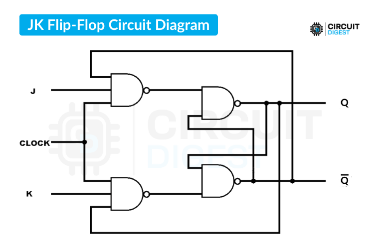
One of the simplest ways to implement an SR flip-flop is using NAND gates.
Above, you can see the basic circuit diagram of an SR flip-flop made using a combination of NAND gates. You can use any NAND IC, and the result will be the same. Here, we are using four NAND gates to construct the SR flip-flop.
The working is simply a combinational output of the logic gates. If you spend some time mapping the values for each individual logic gate, you should be able to understand it clearly.
According to the truth table, if we initially keep both the Set and Reset inputs LOW, the output will remain in its last state. I would like to add a note that this behavior might vary depending on the setup, especially between simulation and real hardware implementation.
If I make the Set pin HIGH while keeping the Reset pin LOW, that will eventually make Q HIGH and Q̅ LOW. Conversely, if the Reset pin is kept HIGH and the Set pin LOW, you will get LOW at Q and HIGH at Q̅.
Furthermore, if we keep both Set and Reset HIGH, the output will be unpredictable. In more technical terms, a race-around condition will occur, which should be avoided. To overcome that issue, the SR flip-flop was upgraded to a D flip-flop.
Practical Demonstration of SR Flip-Flop
To learn the SR flip-flop in a more practical way, you can refer to the article SR Flip-Flop with NAND Gates: Circuit, Truth Table and Working, which covers the SR flip-flop concept, its truth table, a list of components required, the circuit diagram with explanation, and the working of the SR flip-flop using NAND gates.
How to make SR flip-flop using NAND gates?
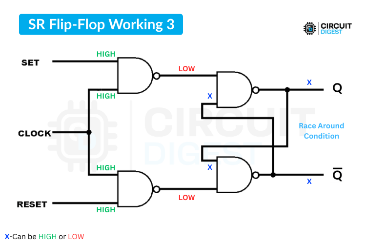
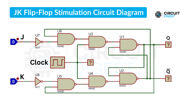
An SR (Set-Reset) flip-flop can be effectively built using NAND gates, as shown in the provided circuit diagram, which utilizes four 7400-series NAND gates. The 7400 chip contains four 2-input NAND gates, each with inputs (e.g., pins 1 and 2) and an output (pin 3). In this setup, two NAND gates form the core latch, while the other two act as input conditioners with the clock signal. The inputs S (Set) and R (Reset) are fed into the first pair of NAND gates alongside the clock signal, ensuring that state changes occur only on clock pulses. The outputs of these gates connect to the second pair, which are cross-coupled to create the latch, producing the Q and Q' (complementary) outputs. This configuration ensures the flip-flop stores a bit of data, setting Q to 1 when S is active or resetting Q to 0 when R is active, all synchronized by the clock.
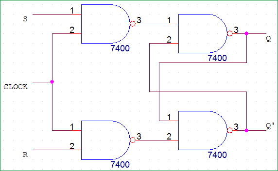
In the diagram, the clock signal enables the flip-flop to update its state only when active (typically high). When the clock is high, the first NAND gate (top left) processes the S input, and the second NAND gate (bottom left) processes the R input. These outputs feed into the cross-coupled NAND gates (right side), which form the latch. If S is 1 and R is 0, the latch sets Q to 1 and Q' to 0; if R is 1 and S is 0, it resets Q to 0 and Q' to 1. When both S and R are 0, the latch holds its previous state, and both being 1 is an invalid condition for an SR flip-flop, as it leads to instability. The use of NAND gates ensures that the circuit operates reliably, with the clock providing precise control over when the flip-flop updates, making it ideal for applications in sequential logic circuits like registers and counters.
D Flip-Flop
The D Flip-Flop is actually an upgrade of the SR Flip-Flop, specifically designed to overcome its major limitation—the invalid state. Unlike the SR Flip-Flop, which requires two inputs (Set and Reset) and may enter an undefined condition when both are high, the D Flip-Flop simplifies the design by using just one input, the D (Data) input.
The operation is straightforward, whatever value is applied to the D input gets stored and reflected at the output Q, but only at the triggering edge of the clock signal (usually the rising edge).
Because it cleanly passes the input to the output in a controlled and predictable way, the D Flip-Flop is widely used in digital electronics, especially in applications like Data storage registers, Pipeline registers in CPUs, Buffering systems, Clocked data transfer circuits
Symbol & Truth Table of D Flip-Flop
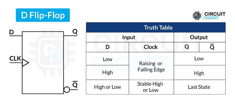
Above, you can see the symbol along with the truth table for the D flip-flop. It is self-explanatory and simple to understand.
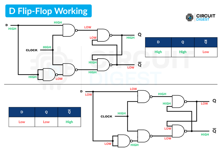
In Simple Terms:
At Clock Edge (↑), the flip-flop copies the D input and holds it until the next tick. That is, if we give HIGH, then Q will be HIGH, and vice versa.
Otherwise, the output stays the same as the previous state.
D Flip-Flop Circuit Working
Among many options for implementing a D flip-flop, I’ll go with the NAND gate version to keep it simple.
Below, you can see the circuit diagram of the D flip-flop, which might look similar to the SR flip-flop.
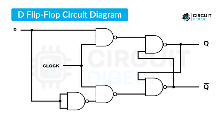
The only difference is that we have used an additional NAND gate as a NOT gate and combined the Set and Reset inputs into a single D input.
Here, as per the combinational logic circuit, Q will be equal to the D input value. If D is HIGH, Q will be HIGH, and Q̅ will be LOW. Similarly, when we provide LOW to the D input, Q will be LOW, and Q̅ will be HIGH. This all happens only at the rising or falling edge of the clock pulse.
If the clock pulse remains at the same logic level (either HIGH or LOW), then regardless of the D input, Q and Q̅ will remain the same as their last state.
Practical Uses of the D Flip-Flop
The D flip-flop is widely used in digital electronics for reliable data storage and synchronization. It forms the core of shift registers, enabling serial-to-parallel data conversion in communication systems. In microprocessors, D flip-flops are essential for building registers to hold temporary data during processing. They’re also used in counters, facilitating frequency division and event sequencing in clocks and timers. Additionally, D flip-flops ensure synchronized data transfer in memory units, preventing timing errors. Their ability to capture and hold data on clock edges makes them indispensable in sequential logic circuits.
If you want to explore the D Flip-Flop in a more practical way, check out the article D Type Flip-Flop: Circuit, Truth Table and Working. It covers the D Flip-Flop basics, truth table, logic gate representation, list of components required, circuit diagram with explanation, a practical demonstration, and even a video to help you understand better.
JK Flip-Flop
The JK Flip-Flop comes with a bit of history behind its name. The most common explanation is that it was just a naming choice used by an engineer in his documentation, maybe based on initials or just random letters that stuck around. Whatever the reason, this flip-flop became popular because it fixed a major issue in the SR Flip-Flop.
It has two inputs, J and K, which function similarly to the Set and Reset inputs in an SR flip-flop, but with a smart upgrade. When both J and K are held HIGH, instead of entering an invalid or unstable state (as seen in the SR flip-flop), the JK flip-flop simply toggles its output. This means if Q is currently LOW, it becomes HIGH, and if Q is HIGH, it becomes LOW. This automatic flipping behavior is what makes the JK flip-flop particularly useful and reliable in sequential circuits.
Because of this, the JK Flip-Flop is perfect for things like counters, digital clocks, and frequency dividers, where the circuit needs to switch states on its own in a clean and timed manner.
Symbol and Truth Table of the JK Flip-Flop
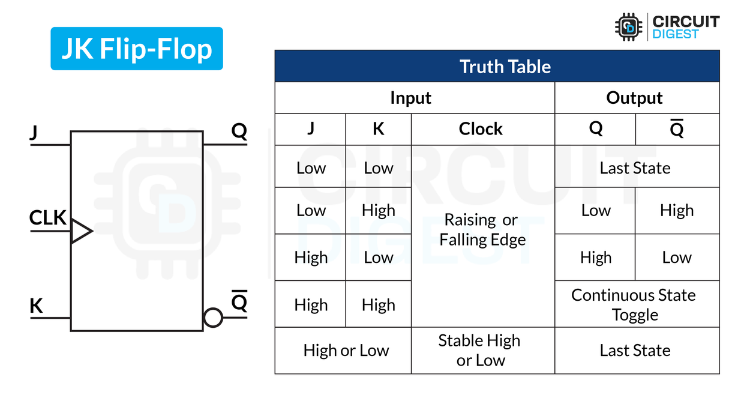
With the above symbol and truth table, you can understand the concept behind the JK flip-flop.
Just like the SR flip-flop, the combinations LOW-LOW, HIGH-LOW, and LOW-HIGH behave the same way. However, if both the J and K inputs are set to HIGH, you will observe a continuous state toggle with each clock pulse. So, let’s move on to the working part to understand it more clearly.
Working Explanation of JK Flip Flop
Like SR and D, it is also possible to implement a JK flip-flop using NAND gates. And that will be appropriate to learn the behavior easily.
Above, you can see the circuit diagram, but with a difference, it uses a 3-input NAND gate. So, it looks a little complex, but it’s actually quite easy.
If you're someone like me who tries to test the circuit using any simulation software like Proteus or Logisim, you might face difficulties in getting the proper output—I did too.
This flip-flop is difficult to simulate with its current combination. So, after some research, I found the circuit diagram below to work well for simulation. This was simulated using Proteus, and it replicates the same JK logic.
This is because, in real-world situations, there are pull-ups and pull-downs responsible for maintaining the active LOW or active HIGH state. But in simulation, it seems to lack such features. Adding them manually also didn’t work on my side.
With this, we can move to the explanation of the working.
Here, most of the logic is similar to the SR flip-flop, which means if you keep both inputs LOW, it will remain in the last state.
And if the J input is kept HIGH and the K is kept LOW, the output Q will be HIGH and Q̅ will be LOW.
Vice versa, if the J input is kept LOW and the K input is kept HIGH, the expected output will be Q LOW and Q̅ HIGH.
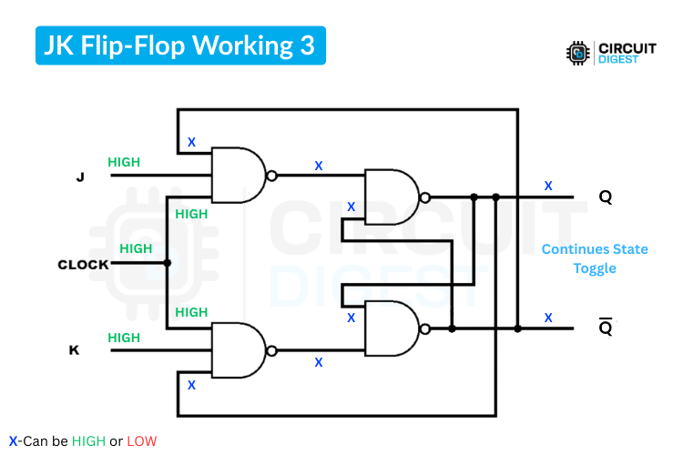
But in the case where both inputs are HIGH, the output will continuously toggle with each clock pulse.
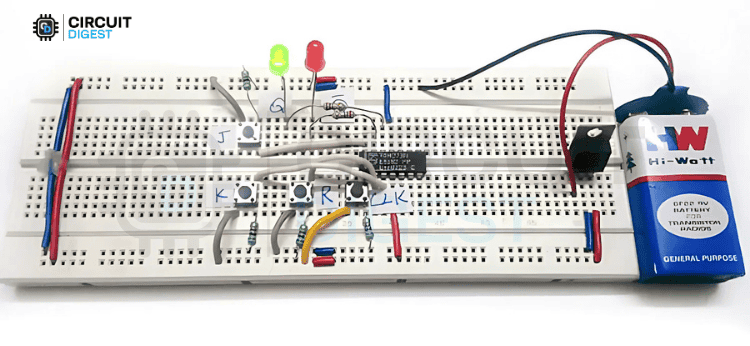
Hope you got to know about the JK flip-flop. Now, in case you are looking to implement this in real-time hardware, we can still make it simple by using dedicated JK flip-flop ICs like 7473, which is often known as MC74HC73A, SN74LS73A, etc. By using this, it’s much easier to implement the JK flip-flop.
Simple explanation of JK flip-flop with Circuit
To explore the representation of JK Flip-Flop using logic gates, a list of components required, the circuit diagram with explanation, and a practical demonstration with working, you can check out the article: JK Flip-Flop: Circuit, Truth Table and Working.
T Flip-Flop
The T Flip-Flop, also known as the Toggle Flip-Flop, is actually a simplified version of the JK Flip-Flop. In fact, it’s like taking a JK Flip-Flop and tying both the J and K inputs together. So instead of two inputs, it has just one—called T (for Toggle).
The working is super simple,
When T = 0, nothing happens. The output stays the same.
When T = 1, the output continuously toggles. IE: If Q = 0, it becomes 1; if Q = 1, it becomes 0, and this cycle repeats on each Clock pulse.
That’s it. This flip-flop is all about flipping the state when told to do so.
Because of its simplicity, the T Flip-Flop is commonly used in binary counters, toggle switches, and control circuits, especially where you want to alternate states with each clock pulse. It’s a neat little component that turns a basic input into reliable, timed output transitions.
Symbol & Truth Table of the T Flip-Flop
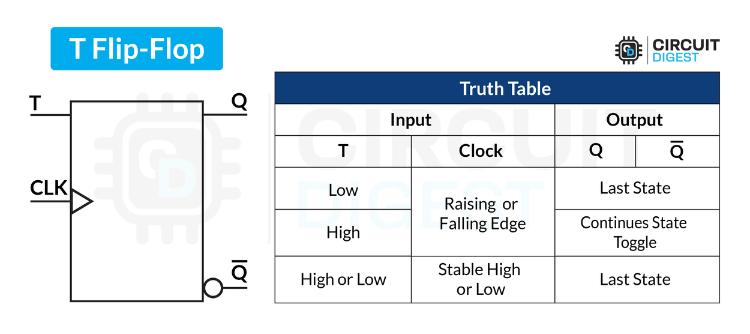
Above you can see the symbol and the truth table for the T Flip-Flop. The T Flip-Flop has just one input, T, and it works based on clock edges—usually the rising edge.
If T is set LOW, the output doesn’t change, no matter how many clock pulses come in. It just holds the previous state.
But when T is set HIGH, the magic happens—on every rising edge of the clock, the output continuously toggles. That means if the current output (Q) is LOW, it becomes HIGH, and if it’s HIGH, it becomes LOW.
T Flip-Flop Circuit Working
As you know, this T Flip-Flop is the extended version of the JK Flip-Flop. Simply tying the J and K inputs of the JK Flip-Flop to the T input makes the T Flip-Flop. Below you can see the circuit diagram of the T Flip-Flop.
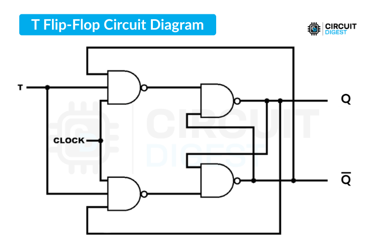
As we already discussed in the JK working section, simulating the same is not easy. I tried different combinations, but finally, it was only possible using the direct JK Flip-Flop IC. So, if you need to do a simulation, you can check it out using the 7473 JK Flip-Flop IC.
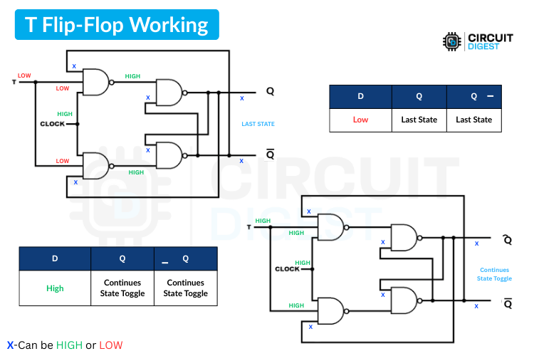
Above you can see the general working of the T Flip-Flop’s combinational logic circuit. As we already discussed, when T is LOW (0), the output stays in its last state, no matter how many clock pulses you give. But when T is HIGH (1), the output toggles on every rising edge of the clock—so if Q was 0, it becomes 1, and if it was 1, it becomes 0.
Just like the JK Flip-Flop, we can use the 7473 IC for demonstrating the T Flip-Flop.
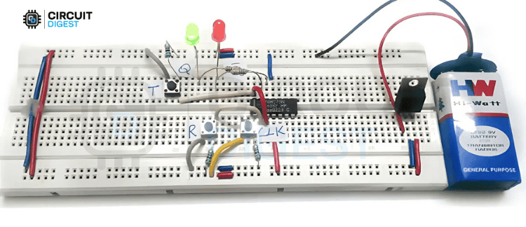
Practical Demonstration of the Toggle Flip-Flop
To dive deeper into the T Flip-Flop, check out the article T Flip-Flop: Circuit, Truth Table and Working. It explains the logic diagram, truth table, and excitation table, compares D and T flip-flops, shows how to convert between D, T, and JK flip-flops, lists the components required, and includes the circuit diagram, working explanation, a practical demo, and even a video to help you understand it clearly.
Comparison between the types of flip-flop
Hope you understand all the types of Flip-Flop Individually in the above sections. Now lets go through a direct brief comparison between each type of flip-flop.
Remember,
SR Flip-Flop is basic but can become unstable when both inputs are HIGH.
D Flip-Flop is ideal for precise data latching, what goes in comes out on clock.
JK Flip-Flop fixes SR's flaws and adds a toggle feature, great for counters.
T Flip-Flop is perfect for flipping states, used widely in frequency division.
Projects on Flip-Flop
These projects offer practical insights into flip-flop applications in digital electronics, helping to understand their use in memory storage, timing circuits, counters, and data synchronization in simple systems.
SR Flip-Flop with NAND Gates: Circuit, Truth Table and Working
Learn how to design an SR flip-flop circuit using NAND gates. This article covers the circuit diagram, working principles, and truth table for a better understanding of SR flip-flops in digital electronics.
T Flip-Flop: Circuit, Truth Table and Working
Learn about T Flip-Flop circuits, including their truth table, working principles, and applications. Explore how this type of flip-flop is used in digital electronics for toggling operations and building counters, with practical circuit examples and clear explanations.
JK Flip-Flop: Circuit, Truth Table and Working
Explore the JK Flip-Flop, its truth table, working principles, and circuit design. Explore its applications in digital electronics, including its use in counters and toggle circuits. Understand how this versatile flip-flop functions with practical examples and clear explanations.
D Type Flip-Flop: Circuit, Truth Table and Working
Understand how the D Flip-Flop works, including its circuit design, truth table, and practical uses. Learn its importance in memory storage and data synchronization with simple explanations and diagrams.
Add New Comment
Wireless Audio Transfer Using LASER Light

In this article, we are going to discuss how to transfer audio through laser light. This is a fun little project, and the concept is similar to what we see in fibre optics cable. We will use a laser light to send data from one point to another. To be particular, in this project here, we are going to transfer our voice from one point to another by shining a laser light on a solar panel. This is made possible by Light Fidelity or (Li-Fi) in short, for those who are new, Li-Fi is a technology in which data can be transferred using light. In our case, we are sending our voice as data and using a Laser as a light source.

![]()
The highlight of this project is its simplicity; you can easily build this over a weekend with commonly available components. If you are interested in Li-Fi, you can also check our Li-Fi Text communication and Li-Fi audio transfer projects.
So, without further delay, let’s dive into building the project.
Discover how to create a project that uses a laser audio transmitter and receiver to wirelessly transmit sound, voice, and music through the use of laser light itself. This project involves the transmission of an LiFi audio transmission to transmit audio data over a focused laser beam, replicating the same technology used in fibre optic communications. Our wireless audio transfer using laser light has been tested and achieves clear audio transmission over indoor distances of 50 meters and outdoor distances greater than 100 meters.
Table of Contents
- How Laser Audio Transmission Works
- └ Transmitter Side
- └ Receiver Side
- Components Required
- Building the Laser Transmitter Circuit
- Transmitter Circuit Construction
- Building the Laser Receiver Circuit
- Testing the LiFi Audio Transmission Project
- Comparison: LiFi vs WiFi vs Bluetooth
- Working Demonstration
- └ Range Testing
- Troubleshooting
- Improvement Ideas & Additional Possibilities
How Laser Audio Transmission Works
Transmitting Audio via Laser light is simpler than it sounds. On the transmitter side, we have a microphone which converts our voice into electrical signals. This signal is then amplified using an audio amplifier, and the output of this amplifier is directly connected to a LASER diode. This light is then pointed towards the solar panel on our receiving circuit. Again, on the receiver side, the solar panel is connected as an audio input for another audio amplifier, which amplifies these signals and plays them on a speaker. All of this works because of the ability of light to carry data. A laser transmitter and receiver system works by converting audio signals into modulated light waves. Understanding this laser audio transmitter circuit operation helps you troubleshoot and optimise your build.
Transmitter Side
→ Audio to Electrical Signal:
We aim to transfer the live audio signal, so in that case, we need some sort of microphone to convert the audio signal to an electrical signal. Actually, speaking, there comes a little bit of a complex circuit to achieve a perfect output. So, to make it simple, we are going to use the MAX4466 Microphone Amplifier Module. You can check out the link if you want to know more about this microphone module. The laser transmitter receiver principle relies on the photoelectric effect.
Above, you can see the GIF video representing the working of the MAX4466 Microphone Amplifier Module. Now we have the electrical signal that needs to be transmitted over the laser.
→ Electric Signal to Laser Beam:
In the above process, we have received the electrical signal. Now this electrical signal is used to drive the laser light beam. It can be done using multiple ways, like using some analog circuits (i.e., switching MOSFET). But to make it simple and more effective, we are using a Mini 5V Audio Amplifier Module based on PAM8403, as you can see in the image below.

The reason behind choosing this is simple. It works in the 5V range, so it can be easily integrated with the MAX4466 Microphone Amplifier Module. It also has an inbuilt potentiometer to adjust the amplitude of the output, and more importantly, it is more affordable. You can use whatever amplifier board you have or even create your own circuits to do the job right. Still, I suggest using the audio amplifier board for better output and hassle-free work. We have previously used the PAM8403 to also build a simple DIY Bluetooth speaker; you can check that out if you are interested.
Now, a laser diode can be connected to the output of the PAM8403 module.

Above, you can see the laser diode we are using. If you would like to reduce the current fed to the laser, you can use a resistor of minimum value. Here, the laser we are using has a built-in 30-ohm resistor in series with the power input. If you feel like reducing the power, you can do so by adding an extra resistor in series or even adjusting the potentiometer in the PAM8403 module.
Receiver Side
→ Laser Light to Electrical Signal:
As in the last step, we have already completed the transmitter side; here we go with the receiver side. So the primary process is to convert the audio signal from the laser light beam to its original state of an electrical signal. Here, generally, we can use any light-based sensor (i.e., LDR, photodiode, etc.) to do the job right, but those with smaller reception areas are quite tough to use. However, they are not unusable; you can even use them. But here in this project, I am going to use a larger array of photodiodes, which is also known as the solar panel.

I am going to use a small toy solar panel. Despite its minimal power output, it is more than enough for our project. So, by using this solar panel, we are going to convert the laser beam to an electrical signal.
→ Electrical Signal to Speaker:
The electrical signal from the solar panel cannot be directly fed to the speaker due to its low power output. Even with a larger solar panel, the small point of light hitting the panel doesn't make a significant change in the output; we will only get a higher DC voltage with a larger panel. However, we need an analog voltage.
To solve this issue, I am going to use the same amplifier module that we used on the transmitter side so that the output electrical signal can be effectively amplified and passed to the speaker.
Regarding the speaker, you can use any speaker compatible with your amplifier module. I am using a 4-ohm, 10-watt speaker, as shown in the image above.
Therefore, we have completed the theory part. I hope you all understand the main concept behind choosing the components and the workings of the project. So, let’s move on to the hardware part of the project.
Components Required for Laser Audio Transmitter Circuit
Below is the list of required components to build the Wireless Audio Transfer using a laser light project. Some components may have alternates. This laser audio transmitter and receiver project uses commonly available components. To learn more about that, read the “Concept of Audio Transfer Via Laser - Explanation” available above.
- Solar Panel - x1
- Laser Diode - x1
- Resistor (30 ohms) - x1
- Potentiometer (100k) - x1
- Speaker (4 ohms, 10W) - x1
- MAX4466 Microphone Amplifier Module - x1
- 7805 5V Voltage Regulator - x2
- PAM8403 Audio Amplifier Module with Potentiometer - x2
- 9V Battery - x2
- BreadBoard - x2
- Jumper Wires - Required Quantity
Building the Laser Transmitter Circuit
Here, this project is built by keeping in mind that to make it easy and use only Minimal components. So, as an outcome, the circuit is simple for Everyone to understand and recreate.
Transmitter Circuit Construction
Here you can see the Schematic of the transmitter part. Those connections are self-explanatory.

We can split the schematic into two parts: The power and Transmitter sections.
⇒ Power Section:
Here, the power source selected is a 9V battery. Since the rest of the circuit operates at 5V, I am using a 7805 5V Linear Voltage Regulator to effectively convert 9V to 5V.
⇒Transmitter Section:
In this section, only four components are being used.
Both the MAX4466 and PAM8403 modules are powered using the 5V output from the voltage regulator. The output of the MAX4466 Microphone Amplifier Module is connected directly to the PAM8403 Audio Amplifier Module.
The PAM8403 supports 2 channels. You can use one channel alone or use both channels as I have. However, we are going to drive only one laser. The laser's positive and negative terminals are connected in parallel with one of the channels. While connecting, I have mentioned using a 30-ohm resistor in series. This is for limiting the current flowing through the laser diode. If you are using the same laser diode as me, this resistor is not needed, as it already has a 30-ohm resistor connected internally.
Building the Laser Receiver Circuit
Below you can see the schematic of the receiver part. You might notice a similar power section here, like the transmitter part, as our requirement is still the same. We are powering the system using 5V. The receiver section of this LiFi audio transmission project converts the optical signal back into audible sound. This laser transmitter and receiver pair demonstrates complete optical communication.

Receiver Circuit Construction
Here, the solar panel’s negative side is grounded, and the positive side is connected to the input of the PAM8403 Audio Amplifier Module. Like the transmitter, I kept both input channels connected. An extra step is applying the bias voltage to the input using a potentiometer, which sets the DC offset to the input of the amplifier. Finally, a speaker is connected to the output of the PAM8403 amplifier module.
That completes our circuit. Next, let us move on to the assembling part.
Testing the LiFi Audio Transmission Project
Let's build the circuit according to our schematic. I am using a breadboard to assemble all the components. Follow this systematic testing procedure to verify that Building the Laser Receiver Circuityour laser audio transmitter and receiver project works correctly.

Above, you can see the assembled image of the transmitter with its parts marked for your reference. The laser diode is directly soldered to a 2x2 Berg strip connector, allowing it to be easily fixed to the breadboard. Similarly, the battery connector is also fitted with a Berg strip for easy breadboard integration.
In this transmitter, there are two configurable areas. One is the gain adjustment in the MAX4466 Microphone Amplifier Module, which controls the sensitivity of the microphone. The other is the amplitude adjustment in the PAM8403 module, which controls the output power to the laser diode. These configurable options allow for precise signal control.

Above, you can see the assembled image of the receiver. Parts like the speaker, solar panel, and battery are connected to the breadboard using Berg male strips, which I have soldered to the wires and fixed to the breadboard.
Like the transmitter, the receiver also has two configurable options. There is a potentiometer connected to the input of the PAM8403 module, which is used to set the DC offset to the input signal. The PAM8403 module itself has a potentiometer to adjust the amplitude of the signal going to the speaker, effectively allowing volume adjustment.
With this, we have completed building the circuit as per the schematic diagram. Next, a Working demonstration.
Comparison: LiFi vs WiFi vs Bluetooth
Understanding where your laser transmitter and receiver technology fits in the wireless communication landscape:
| Feature | LiFi (Laser Audio) | WiFi | Bluetooth |
| Data Rate Potential | High (Gbps theoretical) | Medium-High (Mbps-Gbps) | Low-Medium (Mbps) |
| Range | Medium (10-100m line-of-sight) | High (50-100m through walls) | Low (10-30m through walls) |
| Security | Excellent (cannot penetrate walls) | Good (encryption required) | Good (encryption required) |
| Line-of-Sight Required | Yes (major limitation) | No | No |
| RF Interference | None (uses light) | Moderate (2.4/5GHz congestion) | High (2.4GHz crowding) |
| Power Consumption | Low (LEDs efficient) | Medium-High | Low |
| Latency | Very Low (<1ms) | Low (5-20ms) | Medium (20-100ms) |
| Setup Complexity | High (alignment critical) | Low (automatic) | Very Low (automatic pairing) |
| Ideal Use Cases | Secure rooms, RF-restricted areas, high-bandwidth local transfer | Internet access, networking, general data transfer | Personal devices, audio streaming, IoT |
Working Demonstration of the Wireless Audio Transfer Project
After successfully assembling the components, we began testing the project. It works well both indoors and outdoors, regardless of the conditions. The range of the wireless transfer is impressive, as the intensity of the laser does not diminish significantly under clear weather conditions. As long as the laser beam hits the solar panel, the audio is transferred seamlessly. We also tested the setup from multiple angles and encountered no issues.
The image above was taken while testing the setup outdoors. Unlike other projects, I did not include any GIFs to show the working process, but we have made a video that you can watch below. The video provides a complete demonstration and explanation of the project.
Range Testing
| Environment | Expected Range | Limiting Factors | Optimization Tips |
| Indoor (low light) | 10-50 meters | Ambient light interference, beam dispersion | Test at night, use larger solar panel, shield receiver from room lights |
| Outdoor (clear) | 50-100+ meters | Atmospheric turbulence, precise alignment needed | Use stable mounts, test during calm weather, consider beam collimation lens |
| Outdoor (bright sun) | 5-20 meters | Sunlight overwhelms laser signal | Shade receiver, use IR laser (780nm), add optical filtering |
Troubleshooting Common Issues
Resolve problems with your laser transmitter receiver system using these diagnostic steps:
Problem | Possible Causes | Solutions | Prevention |
No sound from receiver | • Misaligned laser | • Re-aim laser at solar panel center | Use mounting hardware to maintain alignment, mark optimal potentiometer positions |
Distorted/crackling audio | • Excessive transmitter gain | • Reduce MAX4466 gain (turn CCW) | Start with conservative gain settings, test in controlled lighting |
Very weak audio | • Low transmitter gain | • Increase MAX4466 and PAM8403 gain | Use recommended components, avoid cheap undersized solar cells |
Laser not lighting | • Reversed polarity | • Check laser +/- connections | Always use current limiting, verify polarity before powering on |
Intermittent audio | • Vibration/movement | • Secure transmitter/receiver to stable surfaces | Solder permanent connections, use fresh batteries, mount on tripods |
Excessive noise/hum | • Ground loop between units | • Use separate batteries for TX/RX | Use battery power (not wall adapters), add proper filtering from start |
Some of the Improvement Ideas & Additional Possibilities for this Wireless Audio Transfer Project
These are some of my ideas for extending this project, which you can give a try.
Improvement ideas:
Use a more sensitive photodetector instead of a toy solar panel, such as an avalanche photodiode (APD), to improve the reception quality and range.
Implement a focusing lens system to concentrate the laser light on a smaller, more sensitive area of the photodetector.
Introduce noise reduction techniques and filters to improve the audio signal quality.
Some sort of Automatic Alignment System to ensure optimal signal transmission even with movement or misalignment.
Additional Possibilities:
Expand the project to support bidirectional communication by incorporating a similar setup on both ends, allowing two-way audio transmission.
Adapt the system to transmit not only audio but also other types of data, such as digital signals for internet communication, by incorporating appropriate modulation techniques.
Experiment with different laser wavelengths and power levels to extend the effective range of communication, ensuring long-distance transmission capabilities.
Design a compact, battery-operated version of the system for portability, making it suitable for mobile and field applications.
You have successfully built a fully functioning laser audio transmitter and receiver using LiFi technology. This wireless audio transfer using laser light project example illustrates basic ideas and principles of optical communication. The laser audio transmitter circuit serves as a great starting point for additional projects, which may include digital data transmitters, bi-directional communication systems, or long-distance optical links. Share your LiFi audio transmission project experience, ideas and comments, ask questions, and do some additional experiments with optical communications!
Frequently Asked Questions
⇥ 1) Can we use a laser in Li-Fi?
Of course, you can use lasers in a Li-Fi system. Practically, any light source, along with its sensor, can be utilised to create a Li-Fi system.
⇥ 2) Is LiFi Better than Wi-Fi?
Determining whether Li-Fi is better than Wi-Fi depends on various factors. Both have their own pros and cons. For a detailed explanation, visit our article LiFi vs WiFi.
⇥ 3) Is LiFi Safe for Humans?
Yes, LiFi (Light Fidelity) is generally considered safe for humans due to its non-ionising radiation, Low Power Levels, Limited Range, etc. Overall, LiFi is a promising and safe technology for wireless communication, offering a secure and efficient alternative to traditional radio frequency-based systems.
⇥ 4) Advantages and Disadvantages of LiFi?
Advantages of Li-Fi
High-Speed Data Transfer: Li-Fi provides exceptionally fast data transfer rates, often surpassing those of traditional Wi-Fi, by utilising visible light.
Enhanced Security: Since light cannot pass through walls, Li-Fi offers better security against unauthorised access compared to radio frequency systems.
No Radio Frequency Interference: Li-Fi avoids issues related to radio frequency interference, making it suitable for environments sensitive to such interference.
Reduced Latency: Li-Fi can achieve lower latency compared to Wi-Fi, benefiting applications requiring real-time communication and streaming.
Energy Efficiency: Li-Fi can make use of existing LED lighting systems, which are energy-efficient and help lower overall energy consumption.
Disadvantages of Li-Fi
Line-of-Sight Requirement: Li-Fi needs a direct line of sight between the transmitter and receiver, which can limit its range and flexibility.
Limited Range: The operational range of Li-Fi is shorter than that of Wi-Fi due to its reliance on visible light.
Indoor Use Only: Li-Fi is mainly effective in indoor settings where light can be easily managed and controlled.
Light Obstruction: Any blockage or interruption in the light path can disrupt the communication, impacting reliability.
Cost and Infrastructure: Implementing Li-Fi may require higher initial costs and changes to existing infrastructure, such as upgrading to suitable lighting systems.
⇥ 5) What is LiFi Used For?
Li-Fi (Light Fidelity) provides high-speed wireless communication by using visible light, ultraviolet, and infrared radiation for data transmission. It is employed in various settings, such as secure environments where radio frequency (RF) signals are restricted, including military and healthcare facilities. Li-Fi offers fast internet access and can be integrated with LED lighting systems to deliver both illumination and data transfer. It is advantageous in areas with high RF interference and is used to enhance applications like augmented reality (AR) and virtual reality (VR) with its superior bandwidth and low latency.
⇥ 6) What is SLD Laser LiFi?
SLD (Surface Light Emitting Diode) laser Li-Fi refers to a technology that utilises surface-emitting laser diodes to facilitate communication via light. Unlike traditional LEDs that emit light from a single point, SLDs distribute light over a larger surface area, which enhances the efficiency and performance of Li-Fi systems. In SLD laser Li-Fi setups, these laser diodes enable high-speed, high-bandwidth communication using visible light, offering faster data transfer rates compared to conventional LED-based systems. This technology is beneficial for applications demanding rapid data transmission and reliable performance, such as in urban environments and industrial contexts.
⇥ 7) Is laser audio transmission possible outdoors?
Yes. In clear weather, laser audio transmission is generally successful outdoors. The laser will maintain intensity over long distances without visible degradation. However, when establishing a laser audio transmission outdoors, fog, rain or anything else in the direct line of sight between the receiver and transmitter will completely interrupt audio transmission.
⇥ 8) What is the range of a home-built laser audio transmitter?
A simple home-made laser audio transmitter will typically provide audio clarity for around 10-50 meters in indoor conditions, or possibly 100+ meters in outdoor, line-of-sight conditions. The range will be determined by the laser output power, the sensitivity of the solar panel, the interference from the ambient light, and the atmospheric conditions. A more powerful laser will greatly increase the range of the transmitter.
⇥ 9) Is audio transmission using LiFi better than Bluetooth?
LiFi audio transmission encompasses greater bandwidth with no radio interference = however, it requires a direct line of sight. In contrast, Bluetooth is simple, portable, and adaptable. LiFi is preferred for radio frequency sensitive areas, such as hospitals and on an aircraft, while Bluetooth is more relatable to everyday use by consumers.
⇥ 10) What safety protocols are necessary when using laser transmitters?
Under any circumstances, would you want to expose lasers to the eyes, towards aircraft, and at reflective surfaces? If using a laser, then it is recommended to utilise Class 2 or laser systems that pose less than 1mW of risk! Post labelling, beam stops, and carefully constructing the placement of receivers to operate safely with the laser. It is advised not to keep lasers around children. If using a Class 3B or greater, protective eyewear and safety protocols are in place.
Projects in a Similar Realm
We have previously explored Li-Fi Technology in various innovative projects. You can check out the links below to learn more about them.
Audio Transfer using Li-Fi Technology
In this project, we will build a simple circuit to transfer Audio Data using Li-Fi. But first, we will learn about Li-Fi Technology.

The demand for faster and safer internet has made the highly intuitive human brain develop a new wireless technology called Li-Fi. What is this new term, Li-Fi, and how does it differ from Wi-Fi?

Li-Fi-based Text Communication between Two Arduino
Here in this project, we will be demonstrating Li-Fi communication using two Arduinos. Here, the text data is transmitted using an LED and a 4x4 keypad. And it is decoded on the receiver side using LDR. We previously explained Li-Fi in detail and used Li-Fi to transfer audio signals
Add New Comment
How does a Two Way Switch Work - Wiring Connection and Demonstration

One of the simple yet interesting connection diagrams that young engineers learn in their lab is the staircase lighting setup. Perhaps most of us might have already used it without paying much attention to how it works. Staircase lighting at home or at any other place, for that matter, is normally done with something called a two-way switch.
Now, there are many different types of switches in the market, and a few of them can be directly used for a 2 way switch wiring schematic without any special wiring connections. But in this tutorial, we will show you how to make a two-way switch wiring with normal household switches. A two way switching connection means you can control electrical equipment, like a bulb, with two switches placed at different locations, generally used in staircases.
Table of Contents
What is a Two Way Switch Connection?
A two way switch connection is an electrical circuit that allows you to control a single light or appliance from two different locations. A two way switch wiring can be operated from either switch independently, meaning that whatever the position of the other switch (ON/OFF), you can control the light with the other switch. There are two methods of making a two way switch connection diagram: one is the 2-wire control, and the other is the 3-wire control. We have explained both methods below, and both methods are demonstrated in the video given at the end of this article.
Primary Benefits of Two Way Switch Wiring
- Safer Light switch controls: You can control the lights without having to walk through a dark area.
- Convenient Light switch controls: You have a switch when entering and exiting the room.
- Energy efficient: Easy on/off control of mechanical devices may eliminate excess energy use.
- Flexible: Two way switch wiring is compatible with any electrical device: fans, motors, light bulbs.
Two Way Switch Connection Diagram: Understanding the Basics
From the start, we are using the word Two Way switch. Some might know, some not. Let’s see that in brief.
So, technically, a two-way switch is known as a Single Pole Double Throw (SPDT) Switch. Below, you can see some of the Types available in the market.
Some are used in DIY Projects, and some are used in Electrical projects. The following concept is Applicable to all types of applications, from Small DIY Projects to Complex Electrical Wiring Works.
Required Components for Two-Way Switch Connection
2-way switches x 2
Bulb x 1
AC supply x 1
Connecting wires
Two Way Switch Wiring with 2-Wire Configuration
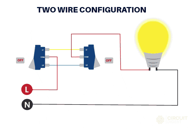
This two way switch wiring schematic represents the traditional method:
This is the first method to make a two way light switch wiring; this is the old method. If you are going to install a new one, then go for three wire control methods.
As you see in the 2 way switch wiring schematic below, you will find that the phase/live is connected with the common of the first 2-way switch. PIN1 & PIN2 of the first switch are connected with the PIN1 & PIN2 of the second switch, respectively. One end of the bulb is connected with the Common Terminal of the second switch, and another end of the Bulb is connected with the Neutral line of the AC power supply.
Note: In the 2-wire control method, when switches are in an opposite state, the light will be in the OFF state as shown in the circuit below:
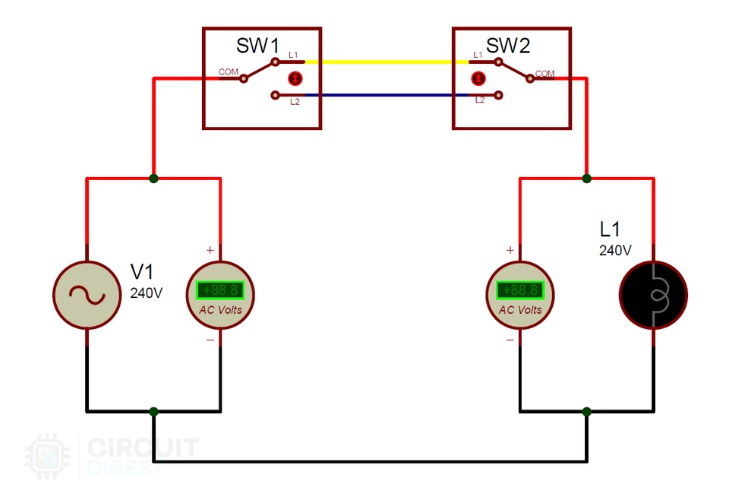
The condition of getting Output in the ON condition is the same as the Ex-nor gate truth table, which is given below:
| Switch 1 (SW1) | Switch 2 (SW2) | Lamp state (L1) |
| OFF | OFF | ON |
| ON | OFF | OFF |
| ON | ON | ON |
| OFF | ON | OFF |
Two Way Switch Connection Diagram with 3 Wires
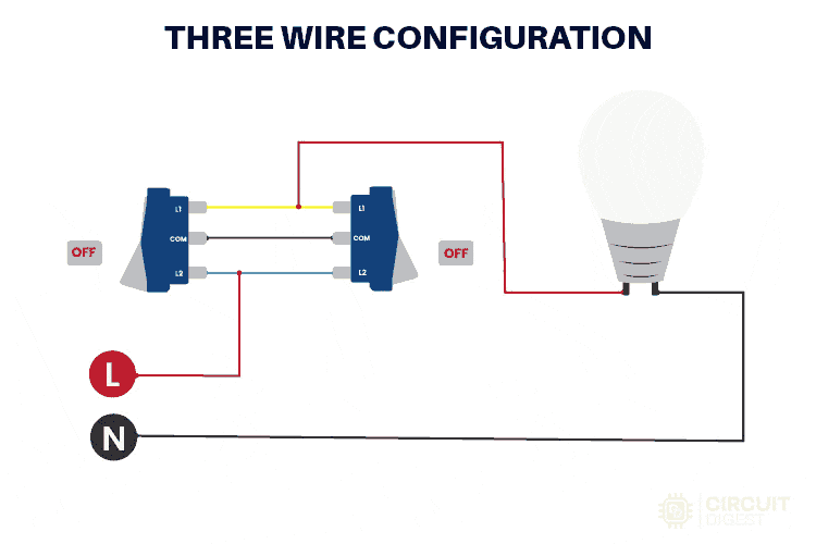
This is the new method to make a two way switch connection diagram with 3 wires, and it is slightly different from the two-wire control method. This method is commonly used nowadays as it is efficient than the Two-Wire control system.
As you can see in the 2 way switch wiring schematic below, the common of both switches is short-circuited. PIN1 of both switches are connected with the phase or live wire, and PIN2 of both switches is connected with one end of the lamp. The other end of the Lamp is connected with the Neutral line of the AC power supply.
Note: In the 3-wire control method, when switches are in the same state, the light will be in the OFF state, as shown in the circuit below:
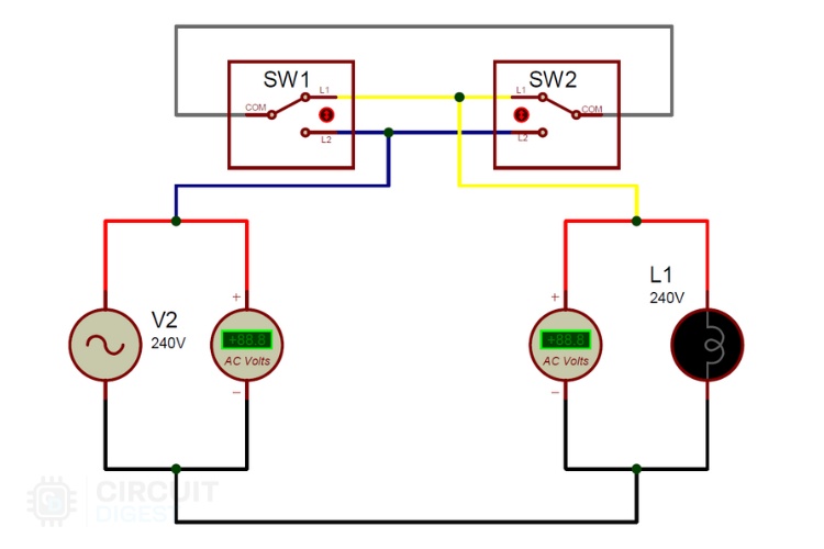
The condition of getting Output in the ON condition is the same as the EX-OR gate truth table, which is given below:
| Switch 1 (SW1) | Switch 2 (SW2) | Lamp state (L1) |
| OFF | OFF | OFF |
| ON | OFF | ON |
| ON | ON | OFF |
| OFF | ON | ON |
Advantages and Disadvantages of these Configurations
Advantages:
Allows control of any appliance from two different areas, regardless of the distance between them. Ideal for locations like staircases, large rooms, and bedrooms where control from multiple points is beneficial. Reduces the need to walk across dark areas to turn lights on or off, enhancing safety.
Disadvantages:
-Increased Wiring: Requires a significant amount of wiring, which can be more complex and costly to install. Diagnosing and fixing issues can be more challenging due to the additional wiring and switch points.
Applications of Two-Way Switch:
Staircases: For controlling lights from both the top and bottom of the stairs.
Erroneous Tripping of Safety/Circuit Protection Equipment: Helps in resetting tripped circuits from different locations.
Large Rooms with Multiple Entry/Exit Gates: Allows for convenient control of lighting or other equipment from different entrances.
Controlling AC Appliances (like fans or lights): Can be controlled from two places, such as the entry and exit points of a room.
Bedrooms: For controlling lights or fans from near the bed or while entering the room, providing convenience and flexibility.
Frequently Asked Questions on Two Way Switch Connection
⇥ In two way switch wiring, what is the difference between three and two wires?
The two-wire is achieved with traveller wires between switches (XNOR logic). The three-wire is achieved with both switches wired to live and load independently (XOR logic). The three-wire is used in new installations.
⇥ Is Wiring a Two-Way Switch Permitted?
You don't have to be an electrician to perform simple electrical work, but complicated tasks must be left to the professional. Whatever the case, follow your local electrical and safety codes. Don't forget to turn off the power before beginning any electrical task.
⇥ Why is my two-way switch not functioning properly?
The primary culprits of a two-way switch problem are shorted switches, improper wiring and poor connections. Inspect all connections; inspect the switch for continuity; and ensure the wiring diagram suits your installation method.
⇥ What Wire Gauge is Required for Two-Way Switch Wiring?
Apply 14 AWG to 15-amp circuits and 12 AWG to 20-amp circuits. Ensure the wire gauge meets your circuit breaker size and local electrical codes.
⇥ What is the longest distance for two way switches?
There is no limit, but increased wire runs equate to increased voltage drop and increased cost of installation. Low-voltage or smart switch technology is recommended for very long distances.
Innovative Applications of Electrical Switches
Discover projects built around switch applications, from simple control circuits to advanced automation systems, highlighting their role in everyday electronics.
What is Switch Bouncing and How to prevent it using Debounce Circuit
Simply, we can say that switch bouncing is the non-ideal behaviour of any switch that generates multiple transitions of a single input. Switch bouncing is not a major problem when we deal with power circuits, but it causes significant issues in logic or digital circuits

Remote Controlled Light Switch
Here we will build a Infrared Light Switch with Remote Control which can be operated wirelessly using any IR Remote like TV remote, AC remote etc.

Build Your Own Compact DIY Smart Switch
This project doesn't require you to change switches in your AC switchboards. As the brain of the project, we will be using ESP8266-01, a solid-state relay for safe and efficient AC switching, and to power it all, a Hi-Link power supply.
Video
Comments
It's a age old logic but still a mesmerizing thing to people who doesn't belong to this domain. Thanks for explaining it so clearly.
In the electrician's trade, the two switch location load control is termed a '3-way' system. The wiring schematic conforming to the adopted International Code Council requires a different physical configuration for safety compliance than what is demonstrated in this article.
Thankyou so much.
.I like it
Thank you for this acticle. You solved a problem for me.
Does anyone know how to do this with an led mech like the clipsal 30PBL? I'd like the mech led off when that switch is powering the light.
nice tutorial of new way of two way two place light control connecting but there is one isuue compared to old way - one additional wire leading in parallel to light. this is redundancy every one want to avoid
It is a good explaination thanks
The three wire versions only virtue is having both switches the same way up.
With the two wire version you just turn one switch through 180 degrees and it amounts to the same!
Add New Comment
A Simple Automatic Plant Watering System without Microcontroller

Nowadays, many people are turning towards green solutions to lead healthier lives. Efforts are being made to grow plants, which contribute to maintaining the stability of nature. The key challenge in growing plants is maintenance, particularly ensuring they receive adequate watering. Despite our best intentions, we may forget to water our plants at times. To address this, we have developed a straightforward automatic plant watering system without Arduino. The idea is to use minimal components and reduce complexity, allowing everyone to easily build it. It's an ideal option for anyone who is trying to automatically water their potted plants during a vacation. An automatic plant watering system addresses this issue by watching soil moisture levels and watering exactly when your plants need it. This article explains how to make a simple automatic plant watering system without Arduino. The components are easily available to you, and you will need no programming experience.
This simple automatic watering system for potted plants relies on simple transistor circuits instead of complicated microcontroller-based solutions, making it an easy project to access for beginners while still achieving an incredibly efficient indoor plant watering automation system.
Let’s see how we can do that!
Table of Contents
How Does This Automatic Plant Watering System Work?
The automatic plant watering system using soil moisture sensor is meant for three stages.
- Detection phase: The soil moisture sensor is there to keep a constant check on the water content in the soil, and whenever the soil turns dry, it will put in a HIGH signal.
- Timer phase: The RC timer circuit will generate an adjustable delay within which the watering has to take place.
- Pump control phase: The BC547 signal switching transistors will switch the mini water pump ON and OFF, relating to the signals from the sensor and from the timer.
The use of such transistor configurations keeps the plants' soil from drying out while avoiding excessive watering. This grows to be one of the perfect solutions as an automatic watering system for potted plants indoors or for balconies outdoors.

Why Choose This Automatic Plant Watering System Project?
- Based on the commonly used BC547.
- Easy to build.
- No need for coding.
- Low-cost design.
- Easy availability of components.
- Has a built-in adjustable delay function.
Components Required to Build Self Plant Watering System:
Required Components are listed below to build the simple Automatic plant watering system.
- Soil Moisture Sensor - x1
- BC547 - x3
- Electrolytic Capacitor - 680uf - x1
Resistor
○ 10k-x1
○ 1k-x1
○ 500E-x1
- 100k Ohm Potentiometer - x1
- Bread Board - x1
- Mini Water Pump (3-6v) - x1
- Mini Water Tube suitable for pump- Required Length.
- 5V Power Source - Any
Automatic Plant Watering System Circuit Diagram Explained
Below is the circuit diagram of the Automatic plant watering system. As you can see, this circuit diagram was so simple and beginner-friendly. If you are not comfortable using components like transistors and resistors, you can try checking out our alternate project, which uses Arduino for an Automatic plant watering system.
Here, the soil moisture sensor is the main component to detect the presence of water in the soil. You can visit our well-written article to learn how the soil moisture sensor works. You may think that with the addition of a single transistor to switch the motor, our circuit can be completed, but there are still two transistors used. It looks simple at the beginning, but if you think carefully, there is a problem that if the motor is turned on for a very short duration, it might trigger the motor more often, and there will be a need for proper watering of the plant. The automatic plant watering system circuit diagram presented below features a beginner's setup for constructing an automatic plant watering system that anyone can use. This automatic plant watering system for indoor use utilises discrete transistors instead of a microcontroller, avoiding programming issues as the automatic watering system operates reliably.

So, to solve this issue, we are utilising the simplest timer circuit known as the RC Timer, which can be seen below. Depending on the value of the resistor and capacitor, we can make the time delay up to a few seconds. As an advantage, we added a potentiometer to make this time delay adjustable. The heart of this automatic plant watering system project is the resistor-capacitor timer that determines watering duration.

Next, you can understand that the Transistor Q1 is used to discharge the capacitor whenever the HIGH signal is received from the Soil Moisture sensor. The output from the RC Timer is connected to Q2, which here works as an inverter. Therefore, I am using Q3 to drive the motor.
You may confuse Q2 itself, which can drive the motor instead of being an inverter. Yeah, of course, it can be used to drive a motor if your sensor provides a Low for Dryness. But Most of the sensors out there will provide High for Dryness and Low for Wetness. You can refer to the table provided below for a brief understanding.
| Sensor Input | Sensor Output | Inverter Requirement | Expected Water Pump State |
| Wetness | HIGH | YES | OFF |
| Wetness | LOW | NO | OFF |
| Dryness | LOW | YES | ON |
| Dryness | HIGH | NO | ON |
Components Assembly of the Automatic Plant Watering System:
For this self watering system for indoor plants, breadboard construction is recommended for easy troubleshooting and modifications. To make this simple, our preference is to make use of a breadboard. If you want to make it more stable, you can also solder it to a Dotted PCB and keep it in any small enclosure. You can see the assembled image of the components, made in the breadboard below. We increased the length of the Wire given in the water Pump, and talking about the pump, I appreciate you checking the perfectness of the waterproofing of the motor. If not, make a proper seal by yourself using some sort of gum or even hot glue, which works well.

And the main thing we need to discuss here is the power supply. This circuit was made to accept a 5V DC input. There are numerous ways to power this circuit, like using DC Power Adapters, Mobile chargers, Power banks, etc. I am using a Micro USB Breakout Module to power up the circuit using a USB Cable Connected to the power bank, which can be seen below.

Ensure that the Proper Connections are made between the components, and then we can start the installation.
Before integrating the pump into your automatic plant watering system, verify its waterproofing integrity. I have selected a small indoor plant pot and installed the humidity sensor along with the tube from the water pump, and the water pump itself was placed in the bottle with the big mouth so that the motor could be installed straightaway. The remaining circuit was placed near the pot and powered by the power bank. This Setup can be seen below.

This automatic plant watering system is powered by 5V DC, which offers a few power options:
» USB Power Bank: Best for portable use and vacation use (recommended for an automatic watering system for potted plants).
» Mobile Phone Charger: A 5V USB wall adapter for permanent installations.
» DC Power Adapter: 5V regulated for constant use.
» Battery System: A Li-ion cell and boost converter for a completely wireless option.
Automatic Plant Watering System using TinkerCad:
Let's simulate the Automatic Plant Watering System using TinkerCad before moving on to a real-time working demonstration. Before building the physical automatic plant watering system project, you can simulate and test the circuit design using TinkerCAD's online platform:
In the simulation, you'll notice that the working logic appears inverted. This is due to the sensor available in TinkerCad providing an inverted output. However, apart from this inversion, the overall logic and components remain the same.
Working Demo of the Automatic Plant Watering System Project:
As already discussed, this project works by detecting dryness in the soil using a soil moisture sensor and switching ON the mini water pump. Once the water starts flowing from the water storage to the Flowerpot, it will be turned OFF after a certain amount of delay set via the potentiometer once it detects wetness inside the pot. The video below shows how this automatic watering system for potted plants works.
That’s all, we completed our Project. This comprehensive demonstration shows how the automatic plant watering system using a soil moisture sensor operates in real-world conditions
Here are some hacks you can do in this automatic plant waterer project.
You can change the Q3-BC547_General Purpose NPN Transistor to some other NPN transistor to increase the current capacity to drive the higher power motors.
C1 can be changed as per your needs. Using the trial-and-error method, you can find the most suitable one.
You can use a battery system consisting of a Single Li-ion cell, a DC-DC Boost Converter, Battery Charging, and a Protection Circuit to make this project portable.
Apart from this concept of an Automatic Plant Watering system, this circuit has many scopes.
Troubleshooting Common Issues
| Problem | Possible Cause | Solution |
| Pump runs continuously | Sensor output inverted or Q2 transistor faulty | Check sensor output polarity; test Q2 transistor; verify wiring |
| Pump never activates | Power supply issue or transistor not conducting | Verify 5V power at all points; check transistor orientation; test with multimeter |
| Very short watering duration | Capacitor value too small or potentiometer at minimum | Increase capacitor value; adjust potentiometer clockwise |
| Sensor not detecting moisture | Sensor corrosion or poor soil contact | Clean sensor probes; ensure proper insertion depth; check sensor power |
| Weak water flow | Pump voltage insufficient or tubing kinked | Verify 5V at pump terminals; straighten tubing; check for blockages |
Conclusion:
This automatic watering system for potted plants allows both novice and seasoned makers to care for their plants, keeping them healthy and ever watered with ease. This automatic plant watering system without Arduino is a great introduction to electronics and automated gardening. This self watering system for indoor plants provides peace of mind and consistent plant care.
Have you built this automatic plant watering system project? What modifications did you make? Share your results and tips in the comments below or on our forum for discussion to help fellow plant enthusiasts create their own automated watering solutions!
Frequently Asked Questions About an Automatic Plant Watering System
⇥ Q1: How is this different from Arduino-based automatic plant watering systems?
This transistor-based system has no programming, is cheaper ($8-15 compared to $25-35 for Arduino models), and uses very little power. But Arduino systems have more features, such as timed watering, moisture readout displays, and remote access. Pick this project for ease and economy.
⇥ Q2: Is it possible to water multiple plants using one automatic watering system?
Yes, in two ways: you can create separate circuits for each of your plants (these may have different water requirements), or you can use a single pump and a manifold tube with a different valve for each plant. If you'd like to have total independent control over each pot, simply copy the entire circuit for each pot, using only one common 5 V power supply for each circuit.
⇥ Q3: What types of plants are best to use in automatic watering systems?
All potted house plants like an automatic watering system, especially if they like to be watered regularly. You want to find plants that like to be watered, like ferns, peace lilies, pothos, and spider plants. Make sure to alter the length of the water timer depending on how much moisture your plant actually needs. Vary the timer length depending on plants, for example: longer for plants requiring more moisture, and shorter watering for succulents that require less water. If you have an extra drought-resistant plant like a cactus that likes to have its soil dry out, do not use an automatic watering system with those plants, and instead just water them as you are supposed to.
⇥ Q4: Could you explain the process of changing the watering interval for my personal plants?
Please rotate the 100kΩ potentiometer in a clockwise direction; the duration will be longer, and counterclockwise, the duration will be shorter. Start at the middle position, and then check the soil moisture after 2-4 hours following watering. If the soil seems too wet, you'll need to reduce the amount, and if the soil is dry, the test period can be increased. The 680µF capacitor will give roughly 30-90 seconds according to the potentiometer adjustment.
⇥ Q5: Will this system prevent me from overwatering my plants?
Yes, the ground moisture sensor wants to avoid overwatering since it only turns the pump on when the ground is dry; however, the RC timer tells you when to water, but not if the plant is actually flooded. It still requires a proper adjustment to the timer to make sure the soil is optimally watered, and not too much water causes flooding.
⇥ Q6: What is the power consumption I can anticipate with this automatic watering system?
Low power usage: around 50-100mA in standby (monitoring with sensors) and 200-400mA when the pump is on. The system can be powered for 2-3 weeks on typical water cycles with a 10,000mAh power bank. For long-term usage, use a wall plug or solar-powered battery pack.
⇥ Q7: Can I make this without electronics knowledge?
Sure thing! This project is easy to start with, involving only wire connections and breadboard component placement using the circuit diagram. Initial builds do not require soldering. Simple multimeter work assists in troubleshooting, but it is not necessary. Dedicate 1-2 hours to the first-time assembly and testing of your automatic plant watering system.
Discover Exciting Projects in a Similar Realm
If you are interested in building more such projects, check out our collection of Arduino Projects. We have more than 500 projects with Code and Circuit diagrams that you can use to build your projects today.

Simple Soil Moisture Detector Circuit
Build your own soil moisture sensor with an easy-to-follow circuit. In this project, we are going to build a simple Transistor Soil Moisture Detector Circuit. In this circuit, we have used an NPN transistor to detect soil moisture.

Arduino-based Automatic Plant Irrigation System with Message Alert
Learn to create an automatic plant watering system using Arduino and get text message alerts using the Sim800L module. You'll also set up a 16x2 LCD display for feedback.

Low Power IoT-Based Compact Soil Moisture Monitoring Device
Make your own battery-powered smart soil moisture sensor using IoT technology, focusing on the ESP8266 module as the main controller.

Arduino Smart Irrigation System Using ESP32 and Blynk App
Explore a smart irrigation setup with Arduino and ESP32. This project goes beyond soil moisture sensing, incorporating water level, humidity, and temperature sensors. Discover how to use IoT features with Blynk.
Add New Comment
T Flip-Flop: Circuit, Truth Table and Working

The term digital in electronics represents the data generation, processing or storing in the form of two states. The two states can be represented as HIGH or LOW, positive or non-positive, set or reset which is ultimately binary. The high is 1 and low is 0 and hence the digital technology is expressed as series of 0’s and 1’s. An example is 011010 in which each term represents an individual state. Thus, this latching process in hardware is done using certain components like latch or Flip-flop, Multiplexer, Demultiplexer, Encoders, Decoders and etc collectively called as Sequential logic circuits.
So, we are going to discuss about the Flip-flops in digital electronics. The flip flop aka latches can also be understood as Bistable Multivibrator as two stable states. Generally, these latch circuits can be either active-high or active-low and they can be triggered by HIGH or LOW signals respectively.
The common types of flip-flops are,
Out of the above types only JK and D flip-flops are available in the integrated IC form and also used widely in most of the applications. Here in this article we will discuss about T Flip Flop.
T Flip-flop:
The name T flip-flop is termed from the nature of toggling operation. The major applications of T flip-flop are counters and control circuits. T flip flop is modified form of JK flip-flop making it to operate in toggling region.
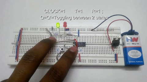
Whenever the clock signal is LOW, the input is never going to affect the output state. The clock has to be high for the inputs to get active. Thus, the T flip-flop is a controlled Bi-stable latch where the clock signal is the control signal. Thus, the output has two stable states based on the inputs which have been discussed below.
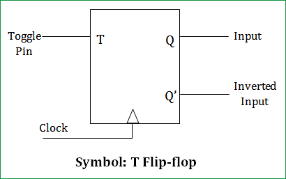
T Flip Flop Logic Diagram
As you know the Flip flops or the latches are made up of multiple logic gates. Here is the logic diagram for a T flip flop, which is basically created using a number of NAND gates. The basic construction of a T flip flop is almost the same as that of a JK flip flop. The only difference is that the J & K inputs are connected together to make the T input.
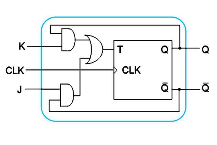
Truth Table of T Flip Flop:
Clock | INPUT | OUTPUT | ||
RESET | T | Q | Q’ | |
X | LOW | X | 0 | 1 |
HIGH | HIGH | 0 | No Change | |
HIGH | HIGH | 1 | Toggle | |
LOW | HIGH | X | No Change | |
The T represents the input while the Q and Q’ represent the output states of the flip-flop. The RESET input is used to reset the outputs to the default stat regardless of the clock or T input. During the normal operation, the RESET pin is held HIGH. During this, the outputs will toggle depending on the T input with a corresponding clock pulse. But, the important thing to consider is all these can occur only in the presence of the clock signal. This, works unlike SR flip Flop & JK flip-flop for the complimentary inputs. This only has the toggling function.
T Flip Flop Excitation Table
The excitation Table tells about the excitation which is required by the flip flop to go from the current state to the next state. Here is the excitation table for the T flip flop. Here, whenever T is 0, Qt+1 is the same as input Q. And, whenever T is 1, Qt+1 is a complement of input Q.
RESET: The RESET pin has to be active HIGH. All the pins will become inactive upon LOW at RESET pin. Hence, this pin always pulled up and can be pulled down only when needed.
D and T Flip Flop Comparison
D flip-flops and T flip-flops serve different purposes in digital circuits, with their primary difference lying in their mode of operation. The D flip-flop is straightforward and is used for storing data. It captures the value present at its D input when a clock pulse occurs, and this value is maintained as the output until the next clock pulse. This characteristic makes the D flip-flop a fundamental building block in registers, shift registers, and various other memory devices, as it reliably stores a single bit of data. On the other hand, the T flip-flop is designed for toggling its output state. With each clock pulse, if the T input is HIGH, the output state changes or toggles. If the T input is LOW, the output remains the same. This behaviour makes the T flip-flop particularly useful in applications like counters and control circuits, where a toggle function is required. In essence, while the D flip-flop serves as a data latch, capturing and holding a bit of data, the T flip-flop acts as a controlled inverter, changing its state only when triggered by its T input.
D flip flop to T flip flop Conversion
The simplest way to convert a D flip flop to a T flip flop is to add an XOR gate to the D input. As the below image shows one input of the XOR gate is fed with the T input while the other input is driven by the output.
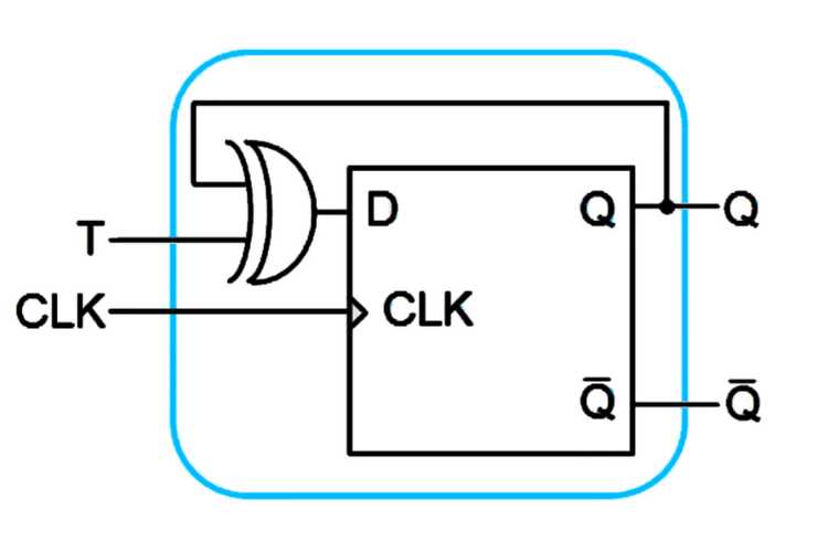
JK flip flop Using T flip flop
Just like we created a D flip flop using the T flip flop, we can also create a JK flip flop using the very same T flip flop. In the input, we have added two AND gates, one input of each of these is connected to the J and K inputs while the other inputs are connected to the outputs Q and ▁Q. The outputs of these AND gets are then fed to an OR gate. The T input is then fed by the output of this OR gate.

T flip flop Using JK flip flop
Creating a T flip flop using a JK flip flop is very simple. All we have to do is connect the J and K inputs together. Here we have used the MC74HC73A (Dual JK-type flip-flop with RESET). It is a 14-pin package which contains 2 individual JK flip-flops inside. The pin diagram and the function of each pin are given below.

| Pin Name | Function |
Q | True Output |
Q’ | Compliment Output |
CLOCK | Clock Input |
J | Data input 1 |
K | Data input 2 |
RESET | Direct RESET (Low activated) |
GND | Ground |
VCC | Supply voltage |
The IC used is MC74HC73A (Dual JK-type flip-flop with RESET). It is a 14 pin package which contains 2 individual JK flip-flop inside. Above are the pin diagram and the corresponding description of the pins. The J and K inputs will be shorted and used as T input.
Components Required:
- MC74HC73A (Dual JK flip-flop) – 1No.
- LM7805 – 1No.
- Tactile Switch – 3No.
- 9V battery – 1No.
- LED (Green – 1; Red – 1)
- Resistors (1kὨ - 3; 220kὨ -2)
- Breadboard
- Connecting wires
T Flip-flop Circuit diagram and Explanation:

The IC power source VDD ranges from 0 to +7V and the data is available in the datasheet. Below snapshot shows it. Also we have used LED at output, the source has been limited to 5V to control the supply voltage and DC output voltage. We have used a LM7805 regulator to limit the LED voltage.
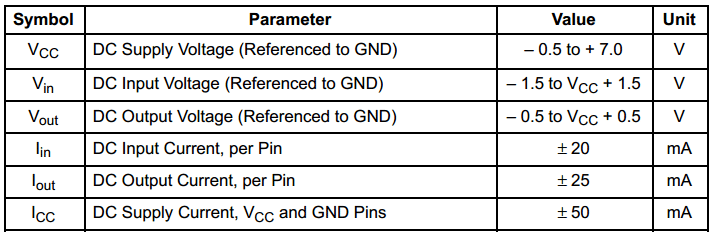
Practical Demonstration of T Flip-Flop:
The buttons T(Toggle), R(Reset), CLK(Clock) are the inputs for the T flip-flop. The two LEDs Q and Q’ represents the output states of the flip-flop. The 9V battery acts as the input to the voltage regulator LM7805. Hence, the regulated 5V output is used as the Vcc and pin supply to the IC. Thus, for HIGH and LOW inputs at T the corresponding output can be seen through LED Q and Q’.
The pins T, CLK are normally pulled down and pin R is pulled up. Hence, default input state will be LOW across all the pins except R which is in High state for normal operation. Thus, the initial state according to the truth table is as shown above. Q=1, Q’=0. The LEDs used are current limited using 220Ohm resistor.
Note: Since the CLOCK is HIGH to LOW edge triggered, both input button should be pressed and hold till releasing the CLOCK button.
Below we have described the various states of T Flip-Flop using a Breadboard circuit with ICMC74HC73A. A demonstration Video is also given below.
State 1:
Clock– HIGH ; T – 1 ; R – 1 ; Q/Q’ – Toggle between two states.
For the State 1 HIGH inputs at T and clock, the RED and GREEN led glows alternatively for each clock pulse (HIGH to LOW edge) indicating the toggling action. The output toggles from the previous state to another state and this process continues for each clock pulse as shown below.
For first clock pulse with T=1
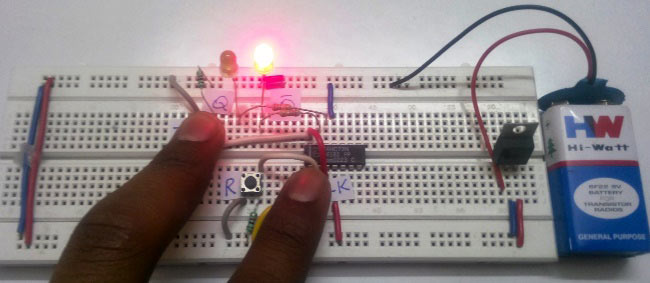
For second clock pulse with T=1
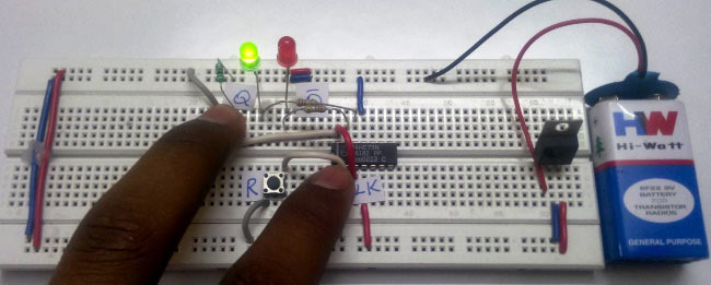
State 2:
Clock– LOW ; T – 0 ; R – 1 ; Q – 0 ; Q’ – 1
The State 2 output shows that the input changes does not affect under this state. The output RED led glows indicating the Q’ to be HIGH and GREEN led shows Q to be LOW. This state is stable and stays there until the next clock and input is applied with RESET as HIGH pulse.
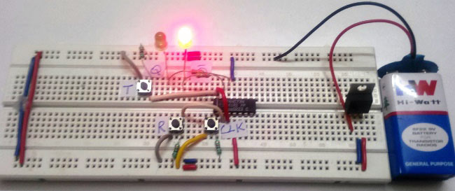
State 3: The remaining states are No change states during which the output will similar to previous output state. The changes do not affect the output states, you can verify with the Truth Table given above.
The complete working and all the states are also demonstrated in the Video below.
Video
Comments
Thank you, very easy to do, and clear lesson, I appreciate your effort. Awesome.
have a wonderful day.
I need to build a very small board with a receiver flip-flop circuit
to operate remotely on and off 20 tiny LEDs in a string. Can you help
I am new to electronics
Thank you
Add New Comment
How to Build a NAND Gate with Transistors?

In the realm of digital electronics and logic circuits, the NAND gates stands as a fundamental cornerstone that wields immense power in information processing. NAND, short for Negated AND, is a logical operation that produces an output of low only when all of its inputs are high.
In this article, we will go over how to build a NAND gate circuit with transistors.
Transistors serve as the building blocks of logic gates, such as AND gates, NAND gates, OR gates, XOR gates, and other gates that are integral to integrated circuits. In our previous electronic circuits, we have perform XOR Gate, NAND Gate, NOT Gate, NOR Gate, AND Gate, OR Gate, XNOR Gate.
By arranging transistors in specific configuration, we can construct the various gates utilized in electronics.
Any type of transistor, be it BJTs or FETs, can be used to create logic gates. However, in this article, we will use NPN BJTs in order to do it. The 2N2222 transistor is a very common and widely available NPN BJT, is capable of acting as either a switch or an amplifier.
What is a NAND logic gate?
A two-input NAND gate produces a LOW output when both of its inputs are HIGH, and a HIGH output otherwise. Creating a NAND gate using only two transistors is relatively straightforward.
NAND Gate Symbol
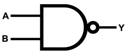
Logic NAND Gates are available using digital circuits to produce the desired logical function and is given a symbol whose shape is that of a standard AND gate with a circle, sometimes called an “inversion bubble” at its output to represent the NOT gate symbol with its logical operation given as.
Truth table of NAND Gate
|
Inputs |
Output |
|
|
A |
B |
Y |
|
0 |
0 |
1 |
|
0 |
1 |
1 |
|
1 |
0 |
1 |
|
1 |
1 |
0 |
Boolean expression for this gate is
Y = A.B
So as you can see from the above truth table, a NAND gate exhibits a HIGH output for all condition except when both inputs are 1. In such a scenario, the output will be a logic LOW.
Components Needed for building NAND gate
So with just the few components, we can construct a NAND gate circuit.
- 2 2N2222 (NPN) transistors
- 2 10kΩ resistors
- 2 220Ω resistors
- 1 470Ω resistor
- 2 Push buttons
- A Breadboard
- A 9V Battery
- LEDs and Connecting wires
Circuit Diagram of NAND Gate using Transistors
The circuit diagram below illustrates the NAND gate using 5 NPN transistors. Here, I1 and I2 represent the two inputs, and O1 signifies the output.

Now, let’s dive into the construction of the NAND gate using two NPN transistors.
- Begin by connecting the collector of the first NPN transistor (Q1) to Vcc (positive voltage) with resistor (RS). This establishes the power connection for Q1.
- Connect the emitter of Q1 to the collector of the second NPN transistor (Q2). This establishes a connection between the two transistors, forming the core of our NAND gate.
- Connect the collector of Q1 to the output terminal Y, which will be our NAND gate’s output.
- Next, attach a resistor (R1) between the base of Q1 and the input terminal A. this resistor limits the current flowing into the base of Q1.
- Connect a resistor (R2) between the base of Q2 and input terminal B. similar to R1, R2 controls the current entering the base of Q2.
A simple 2-input NAND gate can be constructed using RTL Resistor-transistor switches connected together as shown above with the inputs connected directly to the transistor bases. Either transistor must be cut-off “OFF” for an output at Y for turn on the led.
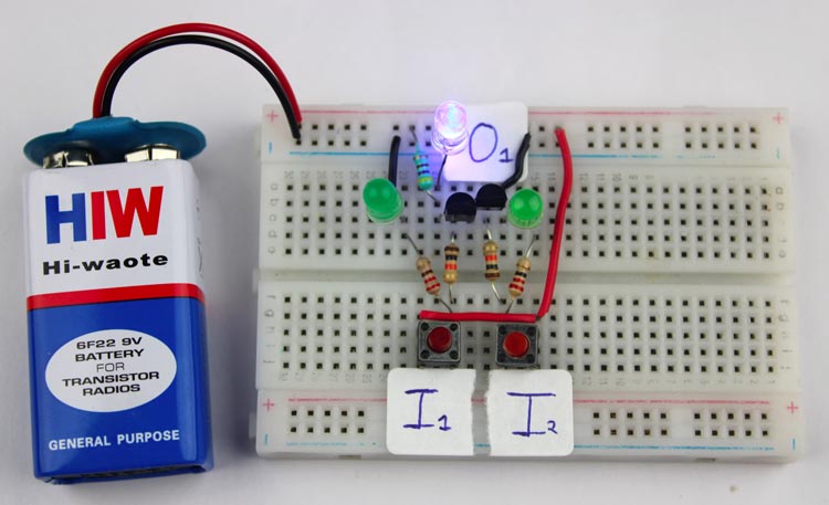
A NAND gate circuit is almost identical to an AND gate circuit. The only key difference is that instead of connecting the output to the emitter of the second transistor, the output is obtained to the collector of the first transistor.
When both inputs are set to HIGH, both transistors conduct through their collector-emitter paths, effectively creating a short circuit to ground. This diverts the current away from the output, which in turn causes the output to go LOW.
Conversely, If either transistor turns off, the supply current is unable to flow through the transistors to the ground. Instead, it flows through the output circuit (Led), resulting in a HIGH output. Hence, the output will be HIGH if either one of the inputs is LOW.
Applications
The NAND gate, with its versatile functionality and ability to negate and simplify logical expressions, finds widespread application in various fields. Some notable application of the NAND gate include Digital logic circuits, universal gate, data storage, error detection and correction, programmable logic controllers (PLCs), digital displays, mathematical and computational operations these are just a few example highlighting the wide-ranging application of the NAND gate. Its versatility, efficiency, and ability to simplify complex logic make it an indispensable component in the design and implementation of digital systems across numerous industries.
Add New Comment
How to Build an XOR Gate with Transistors?

In the vast world of digital electronics and logic circuits, The XOR gate stands as a fundamental building block that plays a crucial role in information processing. XOR, short for Exclusive OR. Is a logical operation that produces an output of high when the number of high inputs is odd, and low when the number of low inputs are even. This unique characteristic makes the XOR gate an essential component in various applications, ranging from simple binary arithmetic to complex data encryption algorithms.
In this article, we will explore the inner working of the XOR gate, including its truth table, logical symbol representation, circuit diagram, and practical construction using transistors.
Previously, we have built many electronic circuits to perform logic gates like XOR Gate, NAND Gate, NOT Gate, NOR Gate, AND Gate, OR Gate, XNOR Gate.
What is an XOR Logic Gate?
The XOR gate is also called the exclusive OR gate. An electronic XOR gate performs the digital logic XOR function. This function is generally similar to the standard OR function with one critical difference. For both OR and XOR, the output is high when either of the two inputs are high, and when both inputs are low, the output is low.
However, when both inputs are set to a high state, the standard OR circuit will produce a high output signal, whereas the XOR circuit will generate a low output signal. This fundamental behavior is the reason behind it is called exclusive OR gate. In the simplest design of XOR gate only 5 transistors are needed.
XOR Gate Symbol

Truth table of XOR gate
|
Inputs |
Output |
|
|
A |
B |
Y |
|
0 |
0 |
0 |
|
0 |
1 |
1 |
|
1 |
0 |
1 |
|
1 |
1 |
0 |
Boolean expression for this gate is
Y = (A ⊕ B)
Output
(A ⊕ B) = A.B + A.B
The truth table above shows clearly demonstrates that the output of an Exclusive-OR gate will only goes “HIGH” when both of its two input terminals are at different logic levels with respect to each other. If these two inputs, A and B are both at logic level “1” or both at logic level “0” the output is a “0”.
Logic Diagram of XOR Gate

As can be seen in the logic diagram above, the Ex-OR gate is built by combining three different types logic gates, the OR gate, the NAND gate and the AND gate to produce the desired result.
Components Needed for building XOR gate
So with just the few components, we can construct a XOR gate circuit.
- 2N2222 (NPN) transistors x5
- 10kΩ resistors x3
- 220Ω resistors x3
- Push buttons x2
- Breadboard x1
- 9V Battery x1
- LEDs and Connecting wires
Circuit Diagram of XOR Gate using Transistors
The circuit diagram below illustrates the XOR gate using 5 NPN transistors. Here, I1 and I2 represent the two inputs, and O1 signifies the output.

The picture shows a simple XOR gate circuit that uses 5 transistors. In the layout inputs A and B are both connected to 9V supply. Different color connecting wires help to see the connections. If there is any ambiguity in the placement of wires the circuit diagram can be referenced.
The gate design is a NAND gate on the left two transistors, a switch for the middle transistors, and an OR gate for the last two transistors.

Upon examining the configuration shown in the photo, it becomes evident that the current generated by the far-right resistor is unable to reach the ground on the lest, resulting in the LED remaining off. The reason behind this lies in the fact that all the current generated by the first resistor on the left is directed towards the first ground. Consequently, the switch remains in the off position due to insufficient voltage entering the base of the third transistor.
In the event that one input is activated, the current gains ability to flow from the far-right transistor to the second ground. Finally, when both inputs are deactivated, the output remains off since the current fails to enter the base of the OR gate transistors. this configuration prevents the current from traveling from the far-right resistor to the second ground.
Applications
From the depth of cryptography to the realm of error detection, the XOR gate proves to be an indispensable ally. It possesses the power to perform bitwise operation, enabling binary addition and subtraction, ensuring data integrity, and even generating parity checks. This gate’s versatility and elegance have solidified its role in countless digital system, paving the way for technological advancements that shape our modern world.
