

The first bipolar junction transistor was invented in 1947 at Bell laboratories. “Two polarities” is abbreviated as bipolar, hence the name Bipolar junction transistor. BJT is a three terminal device with Collector (C), Base (B) and Emitter (E). Identifying the terminals of a transistor requires the pin diagram of a particular BJT part, it will be available in the datasheet. There are two types of BJT - NPN and PNP transistors. In this tutorial we will talk about the NPN transistors. Let us consider the two examples of NPN transistors - BC547A and PN2222A, shown in the images above.
Based on the fabrication process the pin configuration will change and the details will be available in corresponding datasheet. As the power rating of the transistor increases necessary heat sink need to be attached to the body of transistor. An unbiased transistor or a transistor without potential applied at the terminals is similar to two diodes connected back-to-back as shown in figure below.
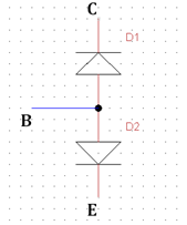
The diode D1 has a reverse conducting property based on the forward conduction of diode D2. When a current flows through the diode D2, the diode D1 senses the current and a proportional current will be allowed to flow in the reverse direction from collector terminal to emitter terminal provided a higher potential is applied at the collector terminal. The proportional constant is the Gain (β).
Working of NPN Transistors:
As discussed above, the transistor is a current controlled device which has two depletion layers with specific barrier potential required to diffuse the depletion layer. The barrier potential for a silicon transistor is 0.7V at 25°C and 0.3V at 25°C for a germanium transistor. Mostly the common type of transistor used are silicon type because silicon is the most abundant element on the earth after oxygen.
Internal operation:
The construction of npn transistor is that the collector and emitter regions are doped with n-type material and the base region is doped with small layer of p-type material. The emitter region is heavily doped when compared with collector region. These three regions form two junctions. They are collector-base junction(CB) and base-emitter junction.
When a potential VBE is applied across Base-Emitter junction increasing from 0V, the electrons and holes start to accumulate at the depletion region. When the potential increases above 0.7V, the barrier voltage is reached and the diffusion occurs. Hence, the electrons flow towards the positive terminal and the base current flows (IB) is opposite to the electron flow. Besides, the current from collector to emitter starts to flow, provided the voltage VCE is applied at collector terminal. The transistor can act as a switch and an amplifier.
Operating region versus Mode of operation:
1. Active region, IC = β×IB – Amplifier operation
2. Saturation region, IC = Saturation current – Switch operation (Completely ON)
3. Cut-off region, IC = 0 – Switch operation (Completely OFF)
Transistor as switch :
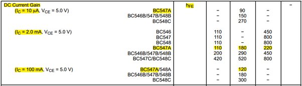
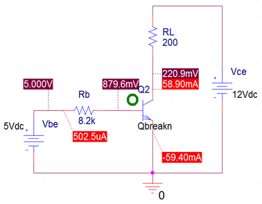
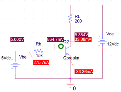
To explain with a PSPICE model BC547A has been selected. The first important thing to bear in mind to use a current limiting resistor at base. Higher base currents will damage a BJT. From the datasheet the maximum collector current is 100mA and corresponding gain(hFE or β) is given.
Steps to select components,
1. Find the collector current wiz the current consumed by your load. In this case it will be 60mA (Relay coil or Parallel LEDs) and resistor = 200 Ohms.
2. In order to drive the transistor into saturation condition sufficient base current has to be supplied such that the transistor is completely ON. Calculating the base current and the corresponding resistor to be used.
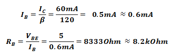
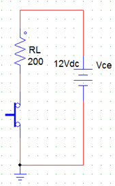
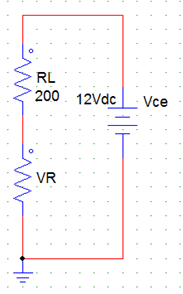
For complete saturation the base current is approximated to 0.6mA (Not too high or too low). Thus below is the circuit with 0V to base during which the switch is OFF state.
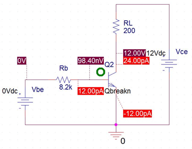
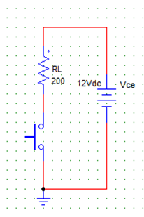
a) PSPICE Simulation of BJT as Switch, and b) equivalent Switch Condition
Theoretically the switch is completely open but practically a leakage current flow can be observed. This current is negligible since they are in pA or nA. For better understanding on current control, a transistor can be considered as a variable resistor across collector(C) and emitter(E) whose resistance varies based on the current through the base(B).
Initially when no current is flowing through base, the resistance across CE is very high that no current flows through it. When an potential of 0.7V & above is applied at base terminal the BE junction diffuses and causes the CB junction to diffuse. Now current flows from collector to emitter based on the gain.
a) PSPICE Simulation of BJT as Switch, and b) equivalent Switch Condition
a) PSPICE Simulation of BJT as Switch, and b) equivalent Switch Condition
The variation of practical value from calculated value is because of the voltage drop across transistor and the resistive load that is used.
Transistor as amplifier :
Amplification is the converting a weak signal into usable form. The process of amplification has been an important step in many applications like wireless transmitted signals, wireless received signals, Mp3 players, mobile phones, and etc., The transistor can amplify power, voltage and current at different configurations.
Some of the configurations used in amplifier circuits are
- Common emitter amplifier
- Common collector amplifier
- Common base amplifier
Of the above types common emitter type is the popular and mostly used configuration. The operation occurs in active region, Single stage common emitter amplifier circuit is an example for it. A stable DC bias point and a stable AC gain are important in designing an amplifier. The name single stage amplifier when only one transistor is being used.
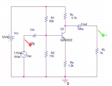
Above is single stage amplifier circuit where a weak signal applied at base terminal is converted into β times the actual signal at collector terminal.
Part purpose:
CIN is the coupling capacitor which couples the input signal to the base of the transistor. Thus this capacitor isolates the source from transistor and allows only ac signal to pass through. CE is the bypass capacitor which acts as the low resistance path for amplified signal. COUT is the coupling capacitor which couples the output signal from the collector of the transistor. Thus this capacitor isolates the output from transistor and allows only ac signal to pass through. R2 and RE provides the stability to amplifier whereas the R1 and R2 together ensures the stability in DC bias point by acting as a potential divider.
Operation:
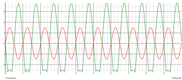
The circuit operates instantaneously for each time interval. Simply to understand, when the ac voltage at base terminal increases the corresponding increase in current flows through the emitter resistor. Thus, this increase in emitter current increases the higher collector current to flow through the transistor which decreases the VCE collector emitter drop. Similarly when the input ac voltage reduces exponentially the VCE voltage starts to increase due to the decrease in emitter current. All these change in voltages reflect instantaneously at the output which will be inverted waveform of the input, but amplified one.
|
Characteristics |
Common Base |
Common Emitter |
Common Collector |
|
Voltage gain |
High |
Medium |
Low |
|
Current gain |
Low |
Medium |
High |
|
Power gain |
Low |
Very High |
Medium |
Table: Gain comparison table
Based on the above table, the corresponding configuration can be utilized.

السلام عليكم ورحمة الله وبركاته
موقع ممتاز وغني بالمعلومات العلمية و المفيدة دروس تسلسلة ومبسطة للمبتدأ
جزاكم الله خيرا على هذه المجهوذات العلمية و المفيذة
واصلو بنشاط احسن
شكرا.