

The SR flip flop using NAND gate truth table is a basic sequential logic circuit that holds one bit of digital information. This extensive guide goes over the general SR flip flop circuit diagram with explanation, a discussion of the truth table, and its implementation using IC SN74HC00N. If you want to become proficient in digital electronics and sequential circuit design, it's important to fully understand the SR flip flop truth table.
Digital electronics is the representation of data processing in two states, a binary representation (HIGH/LOW, 1/0). Sequential logic circuits, like flip-flops, can store and use memory; hence, physical storage of one bit of digital data is possible in digital electronics. Thus, this latching process in hardware is done using certain components like latch or Flip-flop, Multiplexer, Demultiplexer, Encoders, Decoders, etc, collectively called as Sequential logic circuits.
So, we are going to discuss the Flip-flops in digital electronics. The Flip flops can also be understood as a Bistable Multivibrator with two stable states. Generally, these latch circuits can be either active-high or active-low, and they can be triggered by HIGH or LOW signals, respectively.
The common types of flip-flops are,
- RS Flip-flop (RESET-SET)
- D Flip-flop (Data)
- JK Flip-flop (Jack-Kilby)
- T Flip-flop (Toggle)
Out of the above types, only JK and D flip-flops are available in the integrated IC form and are also used widely in most of the applications.
Here in this article, we will discuss about SR Flip Flop and will explore the other Flip Flops in later articles.
Table of Contents
What is an SR Flip Flop? Understanding Sequential Logic Circuits
SR Flip-flops were used in common applications like MP3 players, Home theatres, Portable audio docks, etc. But nowadays, JK and D flip-flops are used instead, due to versatility. SR latch can be built with a NAND gate or with a NOR gate. Either of them will have the input and output complemented to each other. Here we are using NAND gates to demonstrate the SR flip-flop.
The main features of the SR flip flop:
1. Memory: 1 bit of memory
2. Two stable states: Set (Q=1) and Reset (Q=0)
3. Three-state operation controlled by a clock input for synchronised operation
4. Complementary outputs: If Q is high, then Q' is low (they are always complementary states)
5. Retains state using a cross-coupled feedback circuit
Whenever the clock signal is LOW, the inputs S and R never going to affect the output. The clock has to be high for the inputs to get active. Thus, the SR flip-flop is a controlled Bistable latch where the clock signal is the control signal. Again, this gets divided into a positive-edge-triggered SR flip flop and negative negative-edge-triggered SR flip-flop. Thus, the output has two stable states based on the inputs, which have been discussed below.
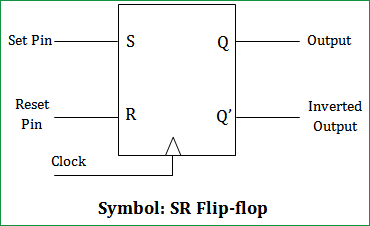
SR Flip Flop Diagram
The figure below shows the basic operation of the SR flip flop diagram in a bistable multivibrator circuit, which has two stable states, making it essential in the circuit design of counters and control applications, especially in modern electronics with memory.
SR Flip Flop Truth Table and Working Principle
The SR flip flop using NAND gate truth table defines how the clock, Set (S'), and Reset (R') inputs relate to the outputs, Q, Q'. The truth table is key to implementing SR flip flop truth table to use in practical designs.
CLK State | INPUT | OUTPUT | ||
Clock | S’ | R’ | Q | Q’ |
LOW | x | x | 0 | 1 |
HIGH | 0 | 0 | 0 | 1 |
HIGH | 1 | 0 | 1 | 0 |
HIGH | 0 | 1 | 0 | 1 |
HIGH | 1 | 1 | 1 | 0 |
Though there are configurations and SR flip flops using NOR gates, in integrated circuits, you will see NAND gate implementations more often. Not only are NAND gates compatible with TTL logic families, but they are also more readily available in fixed packages in various types of logic integration.
The memory size of the SR flip flop using NAND gate truth table is one bit. The S (Set) and R (Reset) are the input states for the SR flip-flop. The Q and Q’ represent the output states of the flip-flop. According to the table, based on the inputs, the output changes its state. But, the important thing to consider is that all these can occur only in the presence of the clock signal.
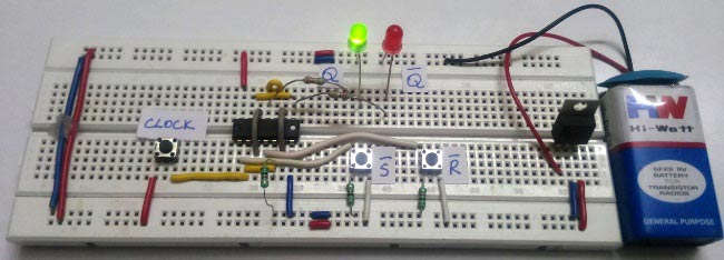
We are constructing the SR flip flop using NAND gate, which is as below,


The IC used is SN74HC00N (Quadruple 2-Input Positive-NAND Gate). It is a 14-pin package which contains 4 individual NAND gates. Below is the pin diagram and the corresponding description of the pins.

Components Required for SR Flip Flop Circuit
Component | Specification | Purpose |
|---|---|---|
IC SN74HC00 | Quad 2-Input NAND Gate | Main logic implementation |
LM7805 | 5V Voltage Regulator | Power supply regulation |
Tactile Switch | SPST Push Button | Clock, Set, and Reset inputs |
LEDs | Green (1), Red (2) | Output indication (Q, Q', Power) |
Resistors | 1kΩ (2), 220Ω (3) | Current limiting, Pull-down |
Battery | 9V DC | Power source |
Breadboard | Standard size | Circuit construction |
Connecting Wires | Jumper wires | Circuit connections |
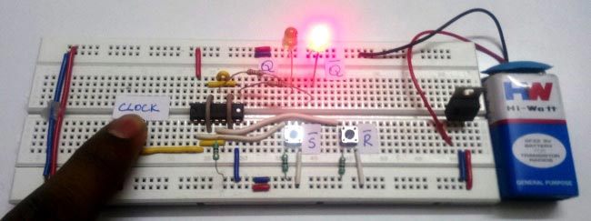
SR Flip Flop Circuit Diagram with Explanation

Here we have used IC SN74HC00N for demonstrating the SR Flip Flop Circuit, which has four NAND gates inside. The IC power source has been limited to a MAXIMUM OF 6V, and the data is available in the datasheet. The snapshot below shows it.
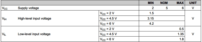
Hence, we have used a LM7805 regulator to limit the supply voltage and pin voltage to 5V maximum.
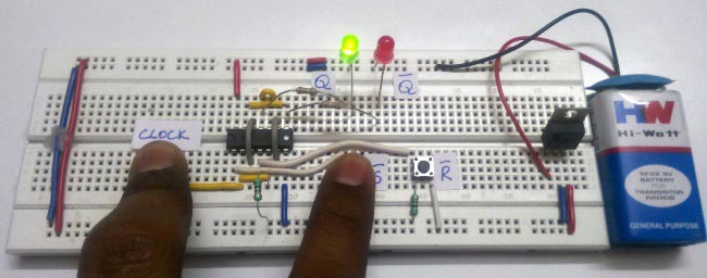
Working States of SR Flip Flop Circuit - Practical Demonstration
The two buttons S (Set) and R (Reset) are the input states for the SR flip-flop. The two LEDs Q and Q’ represent the output states of the flip-flop. The 9V battery acts as the input to the voltage regulator LM7805. Hence, the regulated 5V output is used as the Vcc and pin supply to the IC. Thus, for different inputs at S’ and R’, the corresponding output can be seen through LED Q and Q’.
The truth table and corresponding states vary according to the type of construction, which can be either using NAND gates or NOR gates. Here, it is done using NAND gates. The pins S’ and R’ are normally pulled down. Hence, the default input state will be S’=0, R’=0.
Below, we have described all four states of the SR Flip-Flop using the SR flip-flop circuit made on a breadboard.
State 1⇒ Clock – HIGH ; S’ – 0 ; R’ – 0 ; Q – 0 ; Q’ – 0
For the State 1 inputs, the RED led glows indicating the Q’ to be HIGH, and the GREEN led shows Q to be LOW.
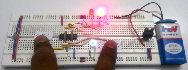
State 2⇒ Clock – HIGH ; S’ – 1 ; R’ – 0 ; Q – 1 ; Q’ - 0
For the State 2 inputs, the GREEN led glows, indicating the Q to be HIG,H and the RED led shows Q’ to be LOW.

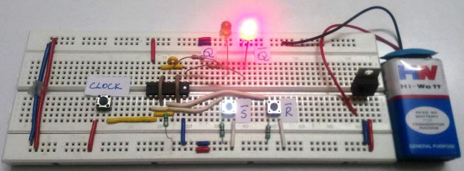
State 3⇒ Clock – HIGH ; S’ – 0 ; R’ – 1 ; Q – 0 ; Q’ - 1
For the State 3 inputs, the RED led glows indicating the Q’ to be HIGH, and the GREEN led shows Q to be LOW.
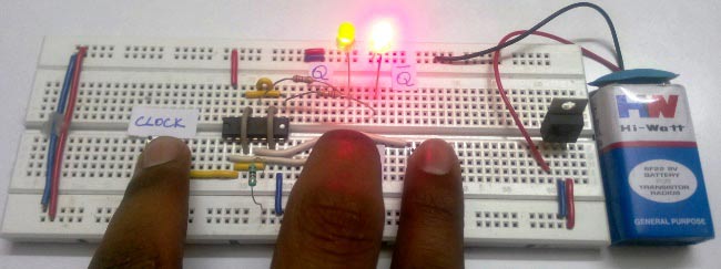
State 4⇒ Clock – HIGH ; S’ – 1 ; R’ – 1 ; Q – 1 ; Q’ - 1
For the State 4 inputs, the RED led and GREEN led glow, indicating the Q & Q’ to be HIGH. But, the state is not stable practically. The output becomes Q=1 & Q’=0 due to instability and absence of a continuous clock.
Comparison: SR Flip Flop Using NOR Gate vs NAND Gate
Parameter | NAND Gate Implementation | NOR Gate Implementation |
|---|---|---|
Input Logic | Active LOW (S', R') | Active HIGH (S, R) |
Normal Input State | S'=0, R'=0 | S=0, R=0 |
Set Operation | S'=1, R'=0 | S=1, R=0 |
Reset Operation | S'=0, R'=1 | S=0, R=1 |
Forbidden State | S'=1, R'=1 | S=1, R=1 |
IC Availability | More Common (TTL Compatible) | Less Common |
Power Consumption | Lower (CMOS NAND) | Higher (CMOS NOR) |
Real World Application
∗ Memory Registers: The basis for the storage of data in processors
∗ Counter Circuits: The basis of binary and decade counters
∗ Control Logic: State machines and sequential control logic
∗ Debouncing Circuits: Must eliminate switch bouncing in digital inputs
∗ Shift Registers: Serial to parallel and parallel to serial translation
Conclusion
The SR flip flop using NAND gate implementation is a basic component within digital electronics that is designed to offer fundamental memory and sequential logic functionality. Familiarity with the SR flip flop truth table, circuit diagram implementation, and real working states allows engineers to create more complex sequential systems such as counters, registers, and state machines.
Although D and JK flip-flops are the preferred digital systems today, the SR flip flop is still important when one wants to study the sequential logic concepts and is the building block for more complex flip-flop designs. One's expertise in the operation, timing parameters, and implementation procedures of the SR flip flop is important if one aims for digital system design and embedded electronics design.
Frequently Asked Questions
⇥ How does the SR flip flop work with NAND gates?
SR flip flop using NAND gates will use cross-coupled NAND gates, with clock control. When the clock is HIGH, the inputs become active. If S = 1, it may either set Q = 1, or if R = 1, it will reset Q = 0. The NAND gate cross-coupled feedback provides a means of state maintenance when the inputs return to 0, creating a bistable memory operation.
⇥ What is the difference between an SR flip flop and an SR latch?
In addition to the inclusion of clock control, the SR flip flop is synchronous (changes state based on the clock), whereas the SR latch is asynchronous and is not controlled by the clock. Flip flop state changes only happen at the edges of the clock, providing better control with timing and turns due to propagation times, while latches are driven immediately and continuously by changes in their respective inputs. The latch is "tied" to the input indefinitely, provided the input logic levels remain unchanged. When directly responding to signals, latches are more sensitive to noise and improper timing issues.
⇥ Why is S=1, R=1 forbidden for the SR flip flop?
When both S = 1 and R = 1, both outputs become 0, and this violates the requirement of complementary outputs (Q and Q' must be opposites). When the inputs return to 0, 0 simultaneously, the output is unstable, and the final Q output is dependent upon the slightest of timing and propagation offsets, yielding unexplained or unexpected behaviour of the expected Flip Flop operation.
⇥ What do the terms setup time and hold time mean in the SR flip flop?
Setup time is the minimum time that the inputs must be stable before the clock edge. Hold time is the minimum time that the inputs must remain stable after the clock edge has occurred. If either setup time or hold time is violated, you may encounter a timing phenomenon known as metastability. This is where the output becomes indeterminate and can cause the circuit in your digital system to be unset.
⇥ What is the way to remove the race condition in the SR flip flop?
Race conditions occur when both S=1 and R=1 occur at the same time. To avoid this occurrence, there are several approaches: substitute a JK flip flop (there is no forbidden state), add priority logic (S takes priority over R, or R takes priority over S), use a master-slave SR flip flop, or design the whole circuit around proper timing with sufficient margin of setup and hold time.
Explore More Digital Logic Circuits
Dive into the core concepts of digital electronics with these foundational logic circuits and tutorials. Whether you're building a full adder or understanding how multiplexers and decoders work, these resources will deepen your grasp of combinational and sequential logic.

Full Adder Circuit and its Construction
In Full Adder Circuit we can add carry-in bit along with the two binary numbers. We can also add multiple bits binary numbers by cascading the full adder circuits which we covered in this tutorial

Multiplexer Circuit and How it Works
In this article we will learn how Multiplexers work, how to design one for our project and also try out a practical example on a breadboard to check the working of a multiplexer circuit hardware.

Learn about decoders, what is a decoder, basic principle of how and why they are used in digital circuits. Find 2:4 decoder, 3:8 decoder, 4:16 decoder and 2:4, 3:8 Priority decoder Circuit, Truth Table and Boolean Expressions.

but we have RS latch no flip-flop.the truth table is also associated to previous Q ,Q`.do this flip flop is edge trigger?