

The term digital in electronics represents the data generation, processing or storing in the form of two states. The two states can be represented as HIGH or LOW, positive or non-positive, set or reset which is ultimately binary. The high is 1 and low is 0 and hence the digital technology is expressed as series of 0’s and 1’s. An example is 011010 in which each term represents an individual state. Thus, this latching process in hardware is done using certain components like latch or Flip-flop, Multiplexer, Demultiplexer, Encoders, Decoders and etc collectively called as Sequential logic circuits.
So, we are going to discuss about the Flip-flops in digital electronics. The latches can also be understood as Bistable Multivibrator as two stable states. Generally, these latch circuits can be either active-high or active-low and they can be triggered by HIGH or LOW signals respectively.
The common types of flip-flops are,
- RS Flip-flop (RESET-SET)
- D Flip-flop (Data)
- JK Flip-flop (Jack-Kilby)
- T Flip-flop (Toggle)
Out of the above types only JK and D flip-flops are available in the integrated IC form and also used widely in most of the applications. Here in this article we will discuss about D type Flip Flop.
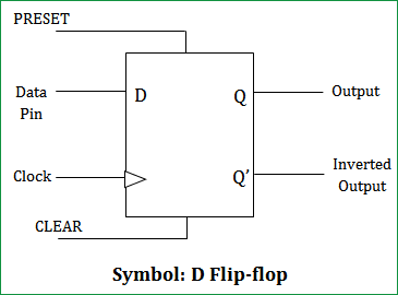
D Flip-flop:
D Flip-flops are used as a part of memory storage elements and data processors as well. D flip-flop can be built using NAND gate or with NOR gate. Due to its versatility they are available as IC packages. The major applications of D flip-flop are to introduce delay in timing circuit, as a buffer, sampling data at specific intervals. D flip-flop is simpler in terms of wiring connection compared to JK flip-flop. Here we are using NAND gates for demonstrating the D flip flop.
Whenever the clock signal is LOW, the input is never going to affect the output state. The clock has to be high for the inputs to get active. Thus, D flip-flop is a controlled Bi-stable latch where the clock signal is the control signal. Again, this gets divided into positive edge triggered D flip flop and negative edge triggered D flip-flop. Thus, the output has two stable states based on the inputs which have been discussed below.
Truth table of D Flip-Flop:
Clock | INPUT | OUTPUT | |
D | Q | Q’ | |
LOW | x | 0 | 1 |
HIGH | 0 | 0 | 1 |
HIGH | 1 | 1 | 0 |
The D(Data) is the input state for the D flip-flop. The Q and Q’ represents the output states of the flip-flop. According to the table, based on the inputs the output changes its state. But, the important thing to consider is all these can occur only in the presence of the clock signal. This, works exactly like SR flip-flop for the complimentary inputs alone.
Representation of D Flip-Flop using Logic Gates:

INPUT | OUTPUT | |
Input 1 | Input 2 | Output 3 |
0 | 0 | 1 |
0 | 1 | 1 |
1 | 0 | 1 |
1 | 1 | 0 |
Thus, comparing the NAND gate truth table and applying the inputs as given in D flip-flop truth table the output can be analysed. Analysing the above assembly as a three stage structure considering previous state(Q’) to be 0
when D = 1 and CLOCK = HIGH
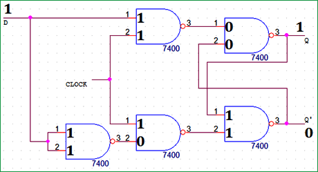
Output : Q = 1, Q’ = 0. Working is correct.
PRESET and CLEAR:
D flip flop has another two inputs namely PRESET and CLEAR. A HIGH signal to CLEAR pin will make the Q output to reset that is 0. Similarly a HIGH signal to PRESET pin will make the Q output to set that is 1. Hence the name itself explain the description of the pins.
Clock | INPUT | OUTPUT | |||
PRESET | CLEAR | D | Q | Q’ | |
X | HIGH | LOW | X | 1 | 0 |
X | LOW | HIGH | X | 0 | 1 |
X | HIGH | HIGH | X | 1 | 1 |
HIGH | LOW | LOW | 0 | 0 | 1 |
HIGH | LOW | LOW | 1 | 1 | 0 |
IC Package:
The IC used here is HEF4013BP (Dual D-type flip-flop). It is a 14 pin package which contains 2 individual D flip-flop in it. Below are the pin diagram and the corresponding description of the pins.

PIN | PIN Description |
Q | True Output |
Q’ | Compliment Output |
CP | Clock Input |
CD | CLEAR-Direct input |
D | Data input |
SD | PRESET-Direct input |
VSS | Ground |
VDD | Supply voltage |
Components Required:
- IC HEF4013BP (Dual D flip-flop) – 1No.
- LM7805 – 1No.
- Tactile Switch – 4No.
- 9V battery – 1No.
- LED (Green – 1; Red – 1)
- Resistors (1kὨ - 4; 220kὨ -2)
- Breadboard
- Connecting wires
D Flip-Flop Circuit Diagram and Explanation:

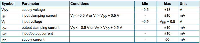
Here we have used IC HEF4013BP for demonstrating D Flip Flop Circuit, which has Two D type Flip flops inside. The IC HEF4013BP power source VDD ranges from 0 to 18V and the data is available in the datasheet. Below snapshot shows it. Since we have used LED at output, the source has been limited to 5V.
We have used a LM7805 regulator to limit the LED voltage.
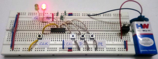
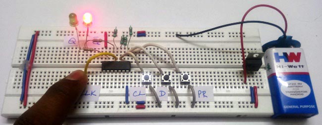
Practical Demonstration of D Flip-Flop:
The buttons D (Data), PR (Preset), CL (Clear) are the inputs for the D flip-flop. The two LEDs Q and Q’ represents the output states of the flip-flop. The 9V battery acts as the input to the voltage regulator LM7805. Hence, the regulated 5V output is used as the Vcc and pin supply to the IC. Thus, for different input at D the corresponding output can be seen through LED Q and Q’.
The pins CLK, CL, D and PR are normally pulled down in initial state as shown below. Hence, default input state will be LOW across all the pins. Thus, the initial state according to the truth table is as shown above. Q=1, Q’=0.
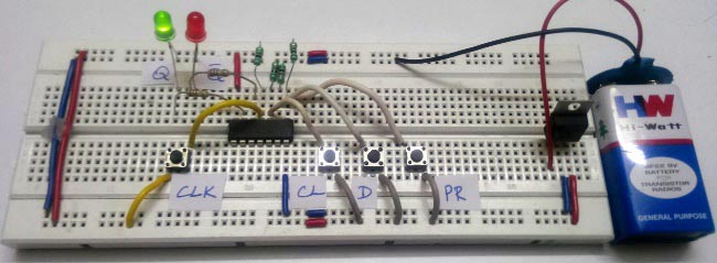
Below we have described the various states of D type Flip-Flop using D flip flop circuit made on breadboard.
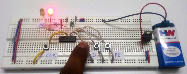
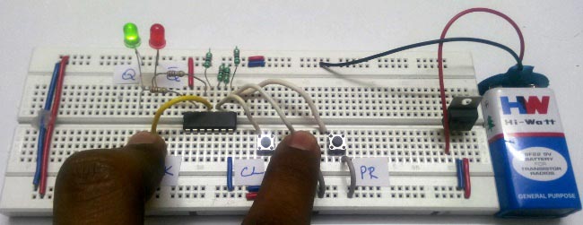
State 1:
Clock – LOW; D – 0 ; PR – 0 ; CL – 1 ; Q – 0 ; Q’ – 1
For the State 1 inputs the RED led glows indicating the Q’ to be HIGH and GREEN led shows Q to be LOW. As discussed above when CLEAR is set to HIGH, Q is reset to 0 and can be seen above.
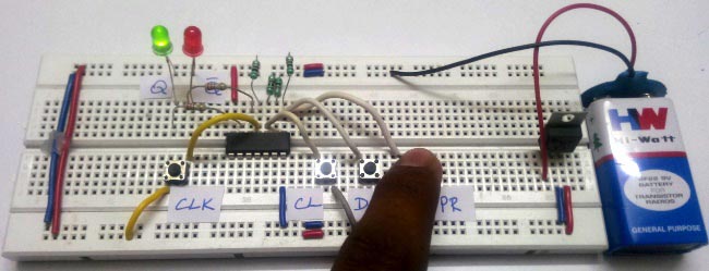
State 2:
Clock – LOW ; D – 0 ; PR – 1 ; CL – 0 ; Q – 1 ; Q’ – 0
For the State 2 inputs the GREEN led glows indicating the Q to be HIGH and RED led shows Q’ to be LOW. As discussed above when PRESET is set to HIGH, Q is set to 1 and can be seen above.
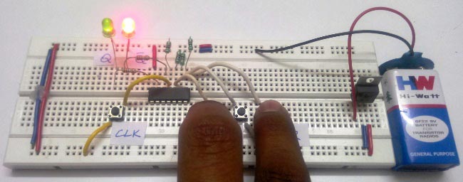
State 3: Clock – LOW ; D – 0 ; PR – 1 ; CL – 1 ; Q – 1 ; Q’ – 1
For the State 3 inputs the RED and GREEN led glows indicating the Q and Q’ to be HIGH initially. When the PR and CL are pulled down on releasing the buttons, the state goes to clear.
State 4: Clock – HIGH ; D – 0 ; PR – 0 ; CL – 0 ; Q – 0 ; Q’ – 1
For the State 4 inputs the RED led glows indicating the Q’ to be HIGH and GREEN led shows Q to be LOW. This state is stable and stays there until the next clock and input. Since the CLOCK is LOW to HIGH edge triggered, D input button should be pressed before pressing the CLOCK button.
State 5: Clock – HIGH ; D – 1 ; PR – 0 ; CL – 0 ; Q – 1 ; Q’ – 0
For the State 5 inputs the GREEN led glows indicating the Q to be HIGH and RED led shows Q’ to be LOW. This state is also stable and stays there until the next clock and input. Since the CLOCK is LOW to HIGH edge triggered, D input button should be pressed before pressing the CLOCK button.

is the clock input edge trigger?falling edge?
but this project is excellent.