

The term digital in electronics represents the data generation, processing or storing in the form of two states. The two states can be represented as HIGH or LOW, positive or non-positive, set or reset which is ultimately binary. The high is 1 and low is 0 and hence the digital technology is expressed as series of 0’s and 1’s. An example is 011010 in which each term represents an individual state. Thus, this latching process in hardware is done using certain components like latch or Flip-flop, Multiplexer, Demultiplexer, Encoders, Decoders and etc collectively called as Sequential logic circuits.
So, we are going to discuss about the Flip-flops in digital electronics. The flip flop aka latches can also be understood as Bistable Multivibrator as two stable states. Generally, these latch circuits can be either active-high or active-low and they can be triggered by HIGH or LOW signals respectively.
The common types of flip-flops are,
Out of the above types only JK and D flip-flops are available in the integrated IC form and also used widely in most of the applications. Here in this article we will discuss about T Flip Flop.
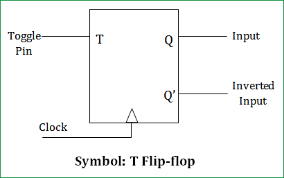
T Flip-flop:
The name T flip-flop is termed from the nature of toggling operation. The major applications of T flip-flop are counters and control circuits. T flip flop is modified form of JK flip-flop making it to operate in toggling region.
Whenever the clock signal is LOW, the input is never going to affect the output state. The clock has to be high for the inputs to get active. Thus, the T flip-flop is a controlled Bi-stable latch where the clock signal is the control signal. Thus, the output has two stable states based on the inputs which have been discussed below.
T Flip Flop Logic Diagram
As you know the Flip flops or the latches are made up of multiple logic gates. Here is the logic diagram for a T flip flop, which is basically created using a number of NAND gates. The basic construction of a T flip flop is almost the same as that of a JK flip flop. The only difference is that the J & K inputs are connected together to make the T input.
Truth Table of T Flip Flop:
Clock | INPUT | OUTPUT | ||
RESET | T | Q | Q’ | |
X | LOW | X | 0 | 1 |
HIGH | HIGH | 0 | No Change | |
HIGH | HIGH | 1 | Toggle | |
LOW | HIGH | X | No Change | |
The T represents the input while the Q and Q’ represent the output states of the flip-flop. The RESET input is used to reset the outputs to the default stat regardless of the clock or T input. During the normal operation, the RESET pin is held HIGH. During this, the outputs will toggle depending on the T input with a corresponding clock pulse. But, the important thing to consider is all these can occur only in the presence of the clock signal. This, works unlike SR flip Flop & JK flip-flop for the complimentary inputs. This only has the toggling function.
T Flip Flop Excitation Table
The excitation Table tells about the excitation which is required by the flip flop to go from the current state to the next state. Here is the excitation table for the T flip flop. Here, whenever T is 0, Qt+1 is the same as input Q. And, whenever T is 1, Qt+1 is a complement of input Q.
RESET: The RESET pin has to be active HIGH. All the pins will become inactive upon LOW at RESET pin. Hence, this pin always pulled up and can be pulled down only when needed.
D and T Flip Flop Comparison
D flip-flops and T flip-flops serve different purposes in digital circuits, with their primary difference lying in their mode of operation. The D flip-flop is straightforward and is used for storing data. It captures the value present at its D input when a clock pulse occurs, and this value is maintained as the output until the next clock pulse. This characteristic makes the D flip-flop a fundamental building block in registers, shift registers, and various other memory devices, as it reliably stores a single bit of data. On the other hand, the T flip-flop is designed for toggling its output state. With each clock pulse, if the T input is HIGH, the output state changes or toggles. If the T input is LOW, the output remains the same. This behaviour makes the T flip-flop particularly useful in applications like counters and control circuits, where a toggle function is required. In essence, while the D flip-flop serves as a data latch, capturing and holding a bit of data, the T flip-flop acts as a controlled inverter, changing its state only when triggered by its T input.
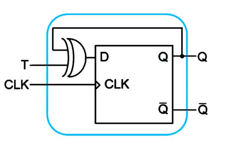
D flip flop to T flip flop Conversion
The simplest way to convert a D flip flop to a T flip flop is to add an XOR gate to the D input. As the below image shows one input of the XOR gate is fed with the T input while the other input is driven by the output.
JK flip flop Using T flip flop
Just like we created a D flip flop using the T flip flop, we can also create a JK flip flop using the very same T flip flop. In the input, we have added two AND gates, one input of each of these is connected to the J and K inputs while the other inputs are connected to the outputs Q and ▁Q. The outputs of these AND gets are then fed to an OR gate. The T input is then fed by the output of this OR gate.

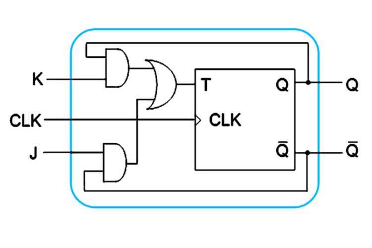
T flip flop Using JK flip flop
Creating a T flip flop using a JK flip flop is very simple. All we have to do is connect the J and K inputs together. Here we have used the MC74HC73A (Dual JK-type flip-flop with RESET). It is a 14-pin package which contains 2 individual JK flip-flops inside. The pin diagram and the function of each pin are given below.

| Pin Name | Function |
Q | True Output |
Q’ | Compliment Output |
CLOCK | Clock Input |
J | Data input 1 |
K | Data input 2 |
RESET | Direct RESET (Low activated) |
GND | Ground |
VCC | Supply voltage |
The IC used is MC74HC73A (Dual JK-type flip-flop with RESET). It is a 14 pin package which contains 2 individual JK flip-flop inside. Above are the pin diagram and the corresponding description of the pins. The J and K inputs will be shorted and used as T input.
Components Required:
- MC74HC73A (Dual JK flip-flop) – 1No.
- LM7805 – 1No.
- Tactile Switch – 3No.
- 9V battery – 1No.
- LED (Green – 1; Red – 1)
- Resistors (1kὨ - 3; 220kὨ -2)
- Breadboard
- Connecting wires
T Flip-flop Circuit diagram and Explanation:

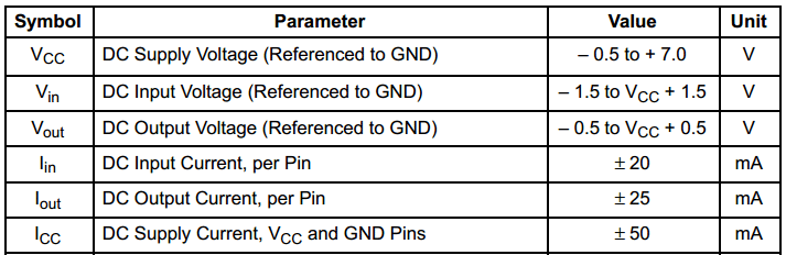
The IC power source VDD ranges from 0 to +7V and the data is available in the datasheet. Below snapshot shows it. Also we have used LED at output, the source has been limited to 5V to control the supply voltage and DC output voltage. We have used a LM7805 regulator to limit the LED voltage.
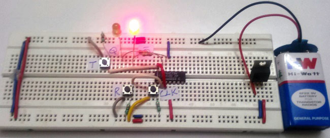
Practical Demonstration of T Flip-Flop:
The buttons T(Toggle), R(Reset), CLK(Clock) are the inputs for the T flip-flop. The two LEDs Q and Q’ represents the output states of the flip-flop. The 9V battery acts as the input to the voltage regulator LM7805. Hence, the regulated 5V output is used as the Vcc and pin supply to the IC. Thus, for HIGH and LOW inputs at T the corresponding output can be seen through LED Q and Q’.
The pins T, CLK are normally pulled down and pin R is pulled up. Hence, default input state will be LOW across all the pins except R which is in High state for normal operation. Thus, the initial state according to the truth table is as shown above. Q=1, Q’=0. The LEDs used are current limited using 220Ohm resistor.
Note: Since the CLOCK is HIGH to LOW edge triggered, both input button should be pressed and hold till releasing the CLOCK button.
Below we have described the various states of T Flip-Flop using a Breadboard circuit with ICMC74HC73A. A demonstration Video is also given below.
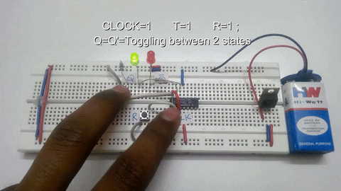
State 1:
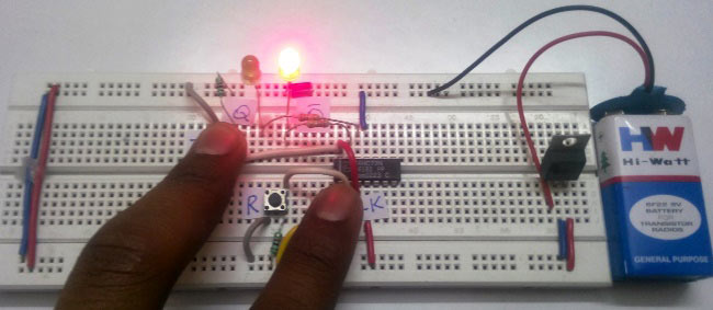
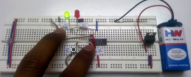
Clock– HIGH ; T – 1 ; R – 1 ; Q/Q’ – Toggle between two states.
For the State 1 HIGH inputs at T and clock, the RED and GREEN led glows alternatively for each clock pulse (HIGH to LOW edge) indicating the toggling action. The output toggles from the previous state to another state and this process continues for each clock pulse as shown below.
For first clock pulse with T=1
For second clock pulse with T=1
State 2:
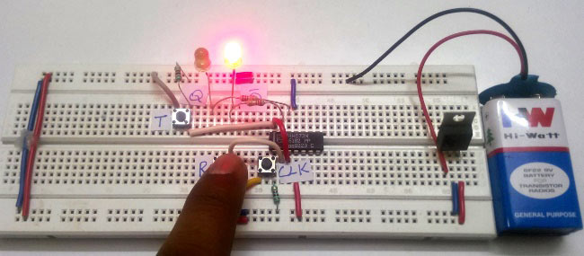
Clock– LOW ; T – 0 ; R – 1 ; Q – 0 ; Q’ – 1
The State 2 output shows that the input changes does not affect under this state. The output RED led glows indicating the Q’ to be HIGH and GREEN led shows Q to be LOW. This state is stable and stays there until the next clock and input is applied with RESET as HIGH pulse.
State 3: The remaining states are No change states during which the output will similar to previous output state. The changes do not affect the output states, you can verify with the Truth Table given above.
The complete working and all the states are also demonstrated in the Video below.
Comments
I need to build a very small board with a receiver flip-flop circuit
to operate remotely on and off 20 tiny LEDs in a string. Can you help
I am new to electronics
Thank you

Thank you, very easy to do, and clear lesson, I appreciate your effort. Awesome.
have a wonderful day.