

The term Multiplexer which is also commonly called as “MUX” or “MPX” refers to selecting one output of the many available inputs. Professor Shankar Balachandran (IIT-M) explains multiplexing as the method of transmitting a large number of information units over a small number of channels or lines and a Digital Multiplexer is a combinational Logic circuit that selects binary information from one of the many input lines and directs it to a single output line.
In this article, we will learn how these Multiplexers work, how to design one for our project and also try out a practical example on a breadboard to check the working on the Hardware.
Basics of Multiplexers:
The best way to understand Multiplexers is by looking at a single pole multi-positioned as shown below. Here the switch has multiple inputs D0, D1, D2 and D3 but it has only one Output (Out) pin. The Control knob is used to select one of the four available data and this data will be reflected on the output side. This way the user can select the required the signal among many available signals.

This is a plain example of a mechanical Multiplexer. But in electronic circuit which involves high speed switching and data transfers we should be able to select the required input very fast using digital circuits. The Control signals (S1 and S0) does exactly the same, they select one input of the many available ones base on the signal provided to them. So the three basic and bare minimum terms on any Multiplexer will be Input Input Pins, Output Pin and Control Signal
Input Pins: These are the available signal pins from which one has to be selected. These signals can either be a digital signal or an analog signal.
Output Pin: A multiplexer will always have only one output pin. The selected input pin signal will be provided by the output pin.
Control/Selection Pin: The Control Pins are used to select the input pin signal. The number of Control pins on a Multiplexer depends on the number of input pins. For example a 4-input multiplexer will have 2 signal pins.
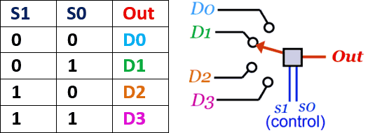
For understanding purpose, let us consider a 4-input multiplexer that is shown above. It has two control signal using which we can select one of the available four input lines. The truth Table below illustrates the status of Control pins (S0 and S1) for selecting the required Input pin.
Now, that we have understood the basic of Multiplexers let’s take a look at the 2-Input Multiplexers and 4-Input Multiplexers which are most commonly used in application circuits.
2-Input Multiplexers:
As the name suggests for a 2-Input Multiplexers we will have 2 Input lines and one Output Lines. Also it will have only one Control pin to select between the available two Input pins. A Graphical representation of a 2:1 Multiplexer is shown below.

Here the input pins are named as D0 and D1 and the Output pin is named as out. The user can select one of the inputs that is either D0 or D1 by using the Control Pin S0. If S0 is kept low (logic 0) then the Input D0 will be reflected on the output pin and if the Input S0 is kept high (logic 1) then the Input D1 will be reflected on the output pin. The truth table representing the same is shown below

As you can see from the table above, when the control signal S0 is 0 the Output reflects the signal values of D0 (highlighted in blue) and similarly when the control signal S0 is 1 the Output reflects the signal values of D1 (highlighted in red). There are few dedicated IC packages which will work as multiplexers straight out of the package, but since we are trying to understand the combinational logic designs, let us build the above 2-input multiplexer by using logic gates. The Logic circuit diagram for the 2-input multiplexer is shown below

The logic diagram utilizes only the NAND gates and hence can be easily build on a perf board or even on a breadboard. The Boolean expression for the Logic diagram can be given by
Out = S0’.D0’.D1 + S0’.D0.D1 + S0.D0.D1’ + S0.D0.D1
We can further simply this Boolean expression by using the cancelling out the common terms, so that the logic diagram gets much more simple and easy to construct. The simplified Boolean expression is given below.
Out = S0’.D0 + S0.D1
Higher Order Multiplexers (4:1 Multiplexer):
Once you understand the working of a 2:1 Multiplexer, it should be easy to also understand the 4:1 Multiplexer. It is just that it will have 4 input pins and 1 output pins with two control lines. These two control lines can form 4 different combinational logic signals and for each signal one particular input will be selected.
The number of control lines for any Multiplexer can be found using the below formulae
2 Number of Control lines = Number of Input lines
So, for instance a 2:1 Multiplexer will have 1 control line because 21 = 2 and a 4:1 Multiplexer will have 2 control lines because 22 = 4. Similarly you can calculate for any higher order Multiplexers.
It is also common to combine to lower order multiplexers like 2:1 and 4:1 MUX to form higher order MUX like 8:1 Multiplexer. Now, for example let us try to implement a 4:1 Multiplexer using a 2:1 Multiplexer. To construct a 4:1 MUX using a 2:1 MUX, we will have to combine three 2:1 MUX together.
The end result should give us 4 Input pins, 2 Control/Select Pins and one output pin. To achieve the first two MUX is connected in parallel and then the output of those two are feeded as input to the 3rd MUX as shown below.


The control/select line of the first two MUX is connected together to form a single line (S0) and then the control line of the 3rd MUX is used as the second control/select signal. Thus finally we get a multiplexer with four inputs (W0, W1, W2 and W3) and only one output (f). The truth table for a 4:1 Multiplexer is shown below.

As you can see in the table above, for each set of value provided to the Control signal pins (S0 and S1) we get a different Output from the input pins on our output pin. This way we can use the MUX to select one among the available four input pins to work with. Normally these Control pins (S0 and S1) will be controlled automatically using a digital circuit. There are certain dedicated IC which can act as MUX and make the job easy for us, so let us take a look at them.
Practical Implementation of Multiplexer using IC 4052:
It is always interesting to build and verify things practically, such that the theory we learn would make more sense. So let us build a 4:1 Multiplexer circuit and check how it works. The IC that we are using here is MC14052B which has two 4:1 Multiplexers inside it. The MC14052B pinout is shown below

Here the pins X0, X1, X2 and X3 are the four input pins and the pin X is its corresponding output pin. The control pins A and B are used to select the required input to the output pin. The Vdd pin (pin 16) has to connect to the supply voltage which is +5V and the Vss and Vee pin should be grounded. The Vee pin is for enable which is an active low pin so we have to ground it to enable this IC. The MC14052 is an Analog Multiplexer meaning the input pins can also be supplied with variable voltage and the same can be obtained though the output pins. The below GIF image shows how the IC outputs variable input voltage based in the control signals provided. The input pins has the voltage 1.5V, 2.7V, 3.3V and 4.8V which is also obtained on the Output pin based on the control signal given.

We can also assemble this circuit over a breadboard and check if they are working. To do that I have used two push buttons are inputs for the control pins A and B. And used a series of potential divider combinations to provide variable voltages for the pins 12, 14, 15 and 11. The output pin 13 is connected to an LED. The variable voltages supplied to the LED will make it to vary the brightness based on the control signals. The multiplexer circuit once build will look something like this below


The complete working video of the multiplexer circuit can also be found at the bottom of this page. Hope you understood the working of Multiplexers and know where to use them in your projects. If you have any thoughts or doubts leave them in the comment section below and I will try my best to respond to them. You can also use the forums to resolve your technical doubts and share your knowledge among other members of this community.
