

An SR latch is a basic memory element in digital electronics that stores binary data using Set and Reset inputs. This tutorial covers the SR latch truth table, the circuit diagram, and the working principle of basic, gated, and clocked SR latch variants.
Initially, after the introduction of transistors, engineers constructed simple latch circuits using transistors. After several stages of evolution, dedicated latches were built using logic gates like the NAND gate and NOR gate. These latches were used to store data, essentially binary data. In this article, we’ll briefly take a look at the SR Latch, along with its Gated SR Latch and Clocked SR Latch versions.
Quick Overview
Duration: 1-2 hours | Type: Digital Logic | Difficulty: Beginner
Technical Scope:
SR latch variants, truth tables, gate circuits
Use Cases:
Memory storage, control flags, data buffering, timing synchronisation
Table of Contents
What is a Latch?
The latch is just a simple bistable circuit and hence has two stable states: set (logic 1) and reset (logic 0). It is a digital circuit that stores one bit of information and retains that output until input variations change it. On the other hand, compared to flip-flops, latches are asynchronous sequential circuits and do not operate with the help of a clock signal. So, output changes occur immediately after the input changes when the latch is enabled.
Key Features of Latches
- Memory unit: Storing one data-bit as long as there is power.
- Asynchronous: There is no clock input; state changes directly with the input.
- Constructed from logic gates: Usually, the gates used will be NAND, NOR, AND, OR, and NOT.
- Basic building blocks of digital systems: They find use in data storage, control circuits, and sequential logic designs.
- Outputs: As the inputs change, outputs keep reflecting that change if it is enabled; else, they hold the stored value.
Types of latches
The primary types of latches that are used in digital circuits and systems
∗ SR Latch
∗ JK Latch
∗ D Latch
∗ T Latch
Let us now discuss the SR Latch in detail.
What is an SR Latch?- Complete Definition
The SR Latch, also known as the Set-Reset Latch, is a fundamental digital memory circuit that stores one bit of binary data using two inputs, namely Set (S) and Reset (R). When Set is activated, the latch outputs '1' (HIGH), and when Reset is activated, it outputs '0' (LOW). The stored value remains stable even after inputs are removed, making it a basic memory element. This latch can be built using either NOR or NAND gates, with the key difference being that NAND implementation uses inverted (active LOW) inputs compared to NOR gates.
Note: If a latch circuit, such as an SR Latch, is edge-triggered using a clock pulse, it becomes a flip-flop. So, ideally, latches and flip-flops are two different things and should not be confused for the same. In our case, if the SR latch is given a clock pulse, it becomes a clocked SR latch, which is also called an SR Flip-Flop.
If you are completely new to flip-flops and latches, check out our tutorial on the Basics of Flip-Flops in Digital Electronics.
More Digital Electronics Tutorials
Sequential Logic Circuits:
SR Latch Quick Reference Guide
| Parameter | Description | Function |
| Set (S) Input | Control input for setting output to HIGH | Forces Q = 1 when activated |
| Reset (R) Input | Control input for resetting output to LOW | Forces Q = 0 when activated |
| Q Output | Primary output representing stored bit | Shows current state (0 or 1) |
| Q̅ Output | Complementary output (inverted Q) | Always opposite of Q in stable states |
Key Elements of SR Latches
- Set (S) Input: Forces Q output to the HIGH state (logic 1)
- Reset (R) Input: Forces Q output to the LOW state (logic 0)
- Q Output: Primary output (representing stored bit)
Sometimes you may also see a Q̅, which is nothing but an inverted output of Q. In the image below, you can see the symbol and a simple SR Latch truth table. From the table, you can notice that the logic is straightforward since it's a memory element.
SR Latch Truth Table - Complete Analysis
The SR latch truth table defines all possible input combinations and corresponding outputs. This table serves as the foundation for understanding SR latch behaviour in digital circuits.
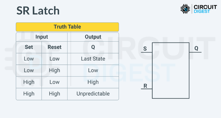
SR Latch Diagram States Explained
There are four possible logic states for this latch:
- When both inputs are LOW, the output remains unchanged. Initially, the output will be undefined (random), but after any other condition is applied, the “both LOW” state will retain the last output.
- When Set is LOW and Reset is HIGH, the output Q goes to the Reset state, which is LOW.
- When Set is HIGH and Reset is LOW, the output Q enters the Set state, which is HIGH.
- In the rare case where both Set and Reset are HIGH, the output Q becomes unstable due to the racing condition. Therefore, this state is considered invalid.
| Set (S) | Reset (R) | Q Output | Q̅ Output | State | Description |
| 0 | 0 | Qprevious | Q̅previous | Hold/Memory | No change - maintains previous state |
| 0 | 1 | 0 | 1 | Reset | Output forced to LOW (0) |
| 1 | 0 | 1 | 0 | Set | Output forced to HIGH (1) |
| 1 | 1 | ? | ? | Invalid/Forbidden | Undefined state - avoid in design |
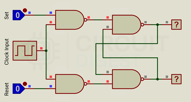
SR Latch Circuit Diagram - NAND and NOR Implementations
The SR latch circuit diagram can be implemented using either NAND gates or NOR gates, each with distinct characteristics and input polarities. Below, you can see a working simulation of a simple SR Latch made using NAND gates, built using Proteus. You can notice how the output values Q and Q̅ change based on the input values S and R.
Now, let’s take a look at the Gated and Clocked versions of the SR Latch.
Gated SR Latch - Enhanced Control Mechanism
For the most part, the gates SR Latch is similar to the standard SR Latch. The only difference is the addition of one extra input, known as Enable. Below, you can see the Gated SR latch truth table and symbol for better understanding.
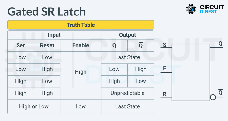
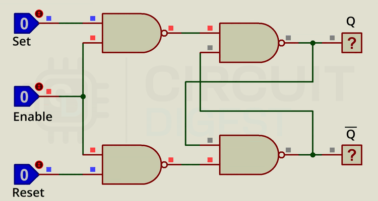
The Enable input allows us to enable or disable the latch, providing more control compared to the basic version. Below is a Gated SR Latch built using NAND logic gates in Proteus. This simulation will help you understand the concept clearly.
The logic here is generally the same as a standard SR Latch, with the only addition being the Enable input.
- If the Enable input is HIGH, the Gated SR Latch works as expected.
- If the Enable input is LOW, regardless of the S and R inputs, the output remains unchanged—in other words, the previous state is held.
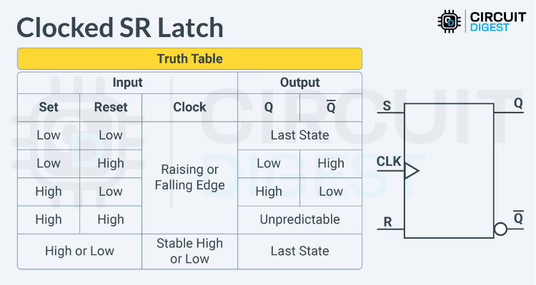
Clocked SR Latch
The Clocked SR Latch, also known as the SR Flip-Flop, is very similar to the Gated SR Latch, except that the Enable input is replaced by a Clock input. Instead of a stable enable line, the output now depends on the rising or falling edge of the clock signal. This is called edge-triggered behaviour.
Below, you can see the symbol and the truth table for a better grasp of the concept.
Clocked SR Latch Benefits
- Edge Triggered: Changes in state occur with the clock transition; the latch is insensitive to the input during any other time
- Noise-Immunity: Glitches get through only when the clock is not transitioning
- Synchronous Operation: Enables timing coordination in consecutive processes
- Timing Predictability: Sidesteps race hazards in systems with complex timing
So, this Clocked SR Latch is essentially an SR Flip-Flop. To learn more about this, you can check out the Flip-Flop in Digital Electronics article for additional information and practical demonstrations. You can also view the simulation result using Proteus in the simulation image below.
As mentioned earlier, the Clocked SR Latch is an edge-triggered device, which makes it more reliable for timed operations in sequential circuits. The working logic is slightly different from that of a regular latch circuit.
To keep it simple, here’s how it works:
- No Change (S = R = 0): The flip-flop retains its previous state.
- Set (S = 1, R = 0): Output Q becomes ‘1’ (Set).
- Reset (S = 0, R = 1): Output Q becomes ‘0’ (Reset).
- Invalid (S = R = 1): Both outputs (Q and Q̅) may become ‘1’, leading to instability. This condition is generally avoided in practical designs.
All these transitions happen only on the positive or negative clock edge, depending on the specific components used in the circuit.
SR Latch Applications in Modern Digital Systems
| Application Domain | Latch Type | Specific Use Cases | Key Benefits |
| Memory Systems | Clocked SR | Cache registers, buffer memory, register files | Fast access, reliable storage |
| Control Logic | Basic SR | State machines, flag registers, event detection | Simple implementation, low cost |
| Communication | Gated SR | UART buffers, protocol controllers, data latching | Controlled access, timing flexibility |
| Timing Circuits | Clocked SR | Clock dividers, frequency synthesis, timing generation | Precise timing, synchronization |
Frequently Asked Questions on SR Latch Table
⇥ 1. What is the difference between an SR latch and a D latch?
An SR latch works with two distinct inputs, Set and Reset, and careful activation of only one of the inputs is required to avoid race conditions. By contrast, a D latch has one data input; the complementing actions take place automatically, hence preventing invalid states and providing a simpler and more reliable operation for digital systems.
⇥ 2. What is invalid for the SR latch if S=1, R=1?
By establishing both inputs of the latch as HIGH and consequently trying to set a 1 at Q and reset a 0 at Q̅, creates an indeterminate state of either 0 or 1. This indeterminate state can initiate an oscillating output and/or lead to unpredictable or undefined behaviour of the circuit. More importantly, the race condition invalidates the fact that Q and Q̅ must be complementary values at any stable output state.
⇥ 3. What is the limiting factor of the SR latch propagation delay?
Propagation delay can restrict switching speed and timing margins. Propagation delay governs the maximum operating frequency of sequential circuits and the setup and hold time, and gated SR latches based on NAND typically achieve about 2-5ns of propagation delay, and NOR is assumed to be slower.
⇥ 4. What will happen to the output of the SR latch at power-on?
The latch will not have a defined output as it will be unpredictable due to component variation, as well as noise at startup. Most latch/systems would contain a power-on reset circuit to force a specific initial state and would likely take advantage of RC networks or power-on reset integrated circuits for reliable startup at system power-on.
⇥ 5. How much power does an SR latch consume?
For CMOS implementations, static power consumption will be almost negligible, with the exception of leakage current; however, dynamic power will depend on switching frequency. At moderate switching speeds, it would be quite minute, about 0.1 - 1 mW. Generally, a NAND implementation will consume less power than the NOR counterparts for most logic families.
⇥ 6. How will temperature affect the SR latch's behaviour?
Increased temperature will increase propagation delays while also compromising noise margins. Commercial-rated devices will be operable within a temperature range of 0 °C - 70 °C, with the industrial counterparts rated -40 °C - 85 °C. Compensation circuits may thus be needed for some applications that require exactness.
⇥ 7. How fast can SR latches operate at?
Most modern CMOS implementations of the SR latch can operate at a frequency of a few GHz, limited by the propagation delay of the latch and parasitic capacitances that result from wiring in the implementation. The practical frequency of operation will depend on what logic family the latch is in: TTL (50 - 100 MHz), CMOS (500 MHz - 2 GHz), and newer processes have demonstrated even greater speeds.
Conclusion
This tutorial covered the fundamental working principle, truth table, and circuit diagrams of basic SR latch, gated SR latch, and clocked SR latch implementations. Understanding these digital logic building blocks is essential for sequential circuit design and memory applications in electronics. If you have any questions, leave them in the comment sections at the bottom of this page, and we will be happy to answer them. You can also join our community or forums to start a discussion.
This tutorial was created by the Circuit Digest engineering team. Our experts focus on creating practical, hands-on tutorials that help makers and engineers master electronic circuit projects.
I hope you liked this article and learned something new from it. If you have any doubts, you can ask in the comments below or use our forum for a detailed discussion.
DIY Projects with SR Flip Flops
If you would like to learn more about SR Flip-Flops, these tutorials include helpful diagrams, truth tables, and logic circuits to guide you through the concepts.

Clocked SR Flip Flop: Complete Guide with Circuit, Truth Table, and Working
Learn how Clocked SR Flip-Flops work using NAND and NOR gates. Includes truth tables, logic diagrams, and real-world timing applications.

SR Flip-Flop with NAND Gates: Circuit, Truth Table and Working
Learn how to build an SR Flip-Flop circuit using NAND gates. Understand the logic, truth table, working principle, and output behaviour with a complete circuit diagram and explanation

What is Switch Bouncing and How to Prevent It Using a Debounce Circuit
Learn how switch bouncing can affect SR Flip-Flop circuits and how to prevent false triggering using debounce techniques like RC filters and Schmitt triggers in digital logic systems.
