

The Clocked SR flip flop is one of the most fundamental sequential logic circuits in digital electronics. Unlike basic SR latches, a clocked SR flip flop circuit uses a clock signal to control when state changes occur, making it essential for synchronous digital systems. This comprehensive guide covers the clocked SR flip flop truth table, circuit diagrams using both NAND and NOR gates, working principles, and practical applications in modern electronics.
Whether you're learning about flip-flops or designing sequential circuits, or troubleshooting memory systems, understanding how a clocked SR flip flop works is crucial for mastering synchronous logic design. We'll explore both positive edge-triggered and level-triggered implementations, compare NAND vs NOR gate designs, and demonstrate real-world applications where precise timing control is essential.
What is a Clocked SR Flip Flop? (Clocked RS Flip Flop)
The Clocked SR flip flop, also called a Clocked RS flip flop or gated SR flip flop, is a synchronous sequential logic circuit that combines the functionality of a basic SR latch with clock-controlled timing. This clock input acts as the heartbeat of the circuit, ensuring that every change in the stored bits happens only during specific clock pulses, making synchronisation between multiple flip-flops much easier than using basic latches. To understand the complete landscape of sequential logic circuits, you can explore our comprehensive guide on Flip-Flop in Digital Electronics: Types, Truth Table, Logic Circuit, and Practical Demonstration.
The Clocked SR (Set-Reset) Flip-Flop or Clocked RS Flip-Flop is an upgraded version of the SR or RS latch, which adds clock synchronisation for better timing control in digital systems. The Clocked SR flip-flop has a total of three inputs:
Set (S)
Reset (R)
Clock (CLK)
Here, during the rising or falling edge of the clock pulse, the flip-flop responds, unlike a latch, which operates continuously.
In the truth table below, the output (i.e., stored data) changes only when an active clock signal is applied. Otherwise, even if S or R is active, the data remains unchanged. This clock-controlled behaviour makes it synchronous and much more reliable for sequential circuit applications.
Clocked SR Flip Flop Truth Table and Symbol
The clocked SR flip flop truth table is essential for understanding how this sequential circuit responds to different input combinations. Below is the complete Clocked SR flip flop diagram showing all possible states of Set (S), Reset (R), Clock (CLK), and the resulting outputs Q and Q̅.
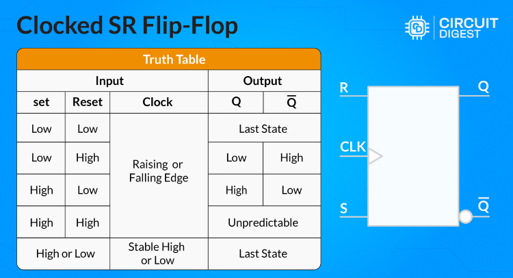
The truth table shows how the flip-flop reacts to different input combinations:
⇒ When the Clock is LOW, the values of S and R don’t matter — the output stays the same as before. No change happens until the clock goes HIGH.
⇒ When the Clock is HIGH, and both the Set and Reset are LOW, the output remains unchanged. It simply holds the previous state.
⇒ When Clock is HIGH, Set is HIGH and Reset is LOW, the output Q becomes HIGH, and Q̅ becomes LOW. This is the Set condition.
⇒ When Clock is HIGH, Set is LOW, and Reset is HIGH, the output Q becomes LOW, and Q̅ becomes HIGH. This is the Reset condition.
⇒ When the Clock is HIGH, and both the Set and Reset are HIGH, the output becomes invalid or unpredictable. This is a forbidden state and should be avoided.
Next, let's take a deeper look at how the Clocked SR (or RS) Flip-Flop works.
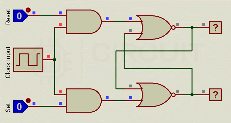
Clocked SR Flip Flop Using NAND Gate
The most common implementation uses NAND gates. For this, a clocked S-R flip-flop is designed by adding two NAND gates to a basic NOR gate flip-flop. The circuit diagram of the Clocked SR (or RS) Flip Flop that uses a NAND Gate is shown below.
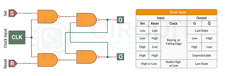
The circuit typically consists of:
A basic SR latch made from NAND gates
Another set of NAND gates that act as clock-controlled switches, along with the S and R inputs
Working Operation in the Clocked SR Flip Flop Using NAND Gate
When the value of the clock pulse is '0', the outputs of both the AND gates will be low, effectively disabling the S and R inputs. This means the flip-flop will hold its previous state regardless of what happens at the S and R inputs.
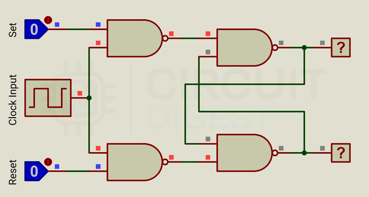
The SR flip-flop works based on basic logic gate combinations. If you follow the signal path through each gate, it’s easy to see how the outputs change. Below, you can see the simulation of the Clocked SR Flip-Flop using NAND gates made in Proteus.
When both Set and Reset are LOW, the output stays the same as before. It's like the flip-flop is remembering its last state. However, this can behave slightly differently in simulations versus real hardware, so keep that in mind.
When Set is HIGH and Reset is LOW, the output Q becomes HIGH, and Q̅ becomes LOW. This is called the "Set" condition.
When Reset is HIGH and Set is LOW, the output Q goes LOW, and Q̅ becomes HIGH. This is the "Reset" condition.
When both Set and Reset are HIGH, this causes an invalid or unpredictable output. It creates a race condition, which can lead to instability, so it's something we should always avoid.
The key advantage of this design is timing control. The SR flip-flop can be used to synchronise data signals between two digital circuits, ensuring that they operate on the same clock cycle. This is useful in communication systems where data needs to be transmitted and received at specific times.
Clocked SR Flip Flop using NOR gate
The Clocked SR Flip-Flop using NOR gates employs NOR gates along with additional AND gates for clock control. In this design, a clocked S-R flip-flop is created by adding two AND gates to a basic NOR gate flip-flop. The circuit diagram of the Clocked SR (or RS) Flip Flop that uses a NOR Gate is shown below.
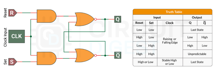
The circuit typically consists of:
Two AND gates that receive the S, R, and Clock inputs
A basic SR latch made from NOR gates
The AND gates act as clock-controlled switches
When the clock pulse goes HIGH (for a positive-edge-triggered flip-flop), the AND gates let the Set (S) and Reset (R) signals pass through to the SR latch inside. From there, the flip-flop behaves just like a regular SR latch:
If S is HIGH and R is LOW, the output Q becomes HIGH.
If S is LOW and R is HIGH, the output Q becomes LOW.
If both S and R are LOW, the output stays the same as before, and it holds the last state.
If both S and R are HIGH, the output becomes unpredictable. This is an invalid condition and should always be avoided.
The working operation of this Clocked SR Flip Flop using NOR Gate can be briefly observed in the GIF video below, which shows the simulation done using Proteus.
Key Advantages of SR Flip-Flops
The main advantage over basic SR latches is that a gated SR latch (or clocked SR latch) can only change its output state when there is an enabling signal along with valid inputs. This prevents unwanted state changes and eliminates timing issues common with asynchronous latches.
Most clocked SR flip-flops are positive edge-triggered, meaning they respond to the rising edge of the clock signal, though some designs may use negative edge-triggering or level-triggering depending on the application.
- Synchronous operations get rid of timing glitches.
- State change control rules out glitches and races.
- Memory function stores one-bit information.
- An accurate timing system is put in place with the clock edge trigger.
- Noise immunity helps to disable the false trigger.
Applications of SR Flip-Flops
Clocked SR Flip-Flops are widely used in digital systems that require synchronised operation, such as:
- Data synchronisation between different circuit blocks
- Memory registers in microprocessors and controllers
- State machines where timing control is critical
- Counter circuits and sequential logic systems
- Control systems that need precise timing coordination
Frequently Asked Questions on Clocked SR Flip Flop
⇥ 1. What is the difference between a clocked SR flip-flop and an SR latch?
A clocked SR flip flop has a clock signal that controls when state changes may occur, whereas an SR latch immediately responds to a change in input. The digital systems use a clock to synchronize events so that unwanted state transitions cannot occur.
⇥ 2. Why is the S=1, R=1 condition forbidden in a clocked SR flip-flop?
The set and reset are entered HIGH simultaneously, which establishes a condition wherein both outputs strive to become LOW, producing unpredictable consequences and possibly an oscillation that may damage the circuit.
⇥ 3. How is clock edge triggering performed with the clocked SR flip-flop?
With fall/rise clock edge triggering, the flip-flop or conditioning circuits respond during selected clock transitions. With this method, it is possible to allow one precise timing instance and speed execution of other actions so that there can be no more changes in state during a current clock pulse period.
⇥ 4. How do you prevent setup and hold time violations in a clocked SR flip-flop?
Your Set and Reset inputs should stabilise before the clock edge (setup time) and hold after the clock edge (hold time). Utilise your timing analysis, and if necessary, insert buffers.
⇥ 5. What is the propagation delay in a clocked SR flip-flop?
Propagation delay is the time from when the clock edge triggers to the time when the output will change. Generally, this takes 5-20 nanoseconds, depending on what your technology is. This will be factored into your maximum operating frequency and other timing calculations often required in digital systems.
⇥ 6. Can the clocked SR flip-flop operate without an external clock signal?
No, the clocked SR flip-flop needs an external clock signal to function properly. Without the clock signal, it acts as a basic latch with always sensitive inputs, effectively losing the advantages of synchronisation.
Exploring Other Flip-Flop Types
Now that you understand the SR flip-flop, you might want to explore other essential flip-flop types that build upon these concepts

T Flip-Flop: Circuit, Truth Table and Working
Learn how a T Flip-Flop works, along with its circuit, truth table, and timing diagram. This guide explains toggle flip-flop operation in digital electronics, comparing it with other types like JK and D flip-flops. Ideal for electronics students and circuit designers exploring sequential logic systems.

JK Flip-Flop: Circuit, Truth Table and Working
Learn how the JK Flip-Flop works with circuit diagrams, truth table, and timing explanation. Understand its toggling behavior and practical applications.

D Type Flip-Flop: Circuit, Truth Table and Working
Explore the working of D Flip-Flops with circuit diagrams, truth table, and timing details. Learn how data is stored and transferred in digital systems.

SR Flip-Flop with NAND Gates: Circuit, Truth Table and Working
Learn how to build an SR Flip-Flop circuit using NAND gates. Understand its working, truth table, and behavior for digital memory and control applications.
T Flip-Flop: Circuit, Truth Table and Working
Explore the T Flip-Flop circuit with working explanation, truth table, and timing diagram. Ideal for frequency division and toggle operations in digital circuits.
