

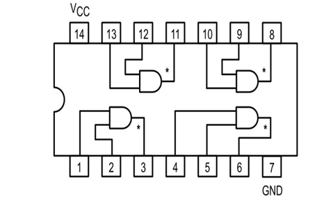
AND logic gate is a digital logic gate, designed for arithmetic and logical operations, every electronic student must have studied this gate is his/her career. This gate is mainly used in applications where there is a need for mathematical calculations. So in calculators, computers and manly digital applications use this gate. Here we are going to use IC 74LS09 for demonstration, this chip has 4 AND gates in it. These four gate are connected internally as shown in below pin diagram.
These gates have limitations for working voltage and input logic frequency. When these limitations are not considered the chip may damage permanently, so one should pay attention while selecting the logic gates.
Components
- Power supply (5v)
- 1K (2 pieces), 220Ω resistors
- 4LS09 QUAD AND GATE IC
- 1 LED
- Buttons (2 pieces)
- 100nF capacitor (2 pieces)
- Breadboard and Connecting wires
Circuit Diagram and Explanation
The truth table of AND gate is show below.
Input A | Input B | Output Y |
H | H | H |
L | X | L |
X | L | L |
As in truth table the output of a AND gate should be HIGH only if both the gate inputs are HIGH. In any other case the output should be LOW. So if any one or both inputs are LOW the output of AND gate will be LOW.
In this circuit we are going to pull down both input of a gate to ground through a 1KΩ resistor. And then the inputs are connected to power through a button. So when the button is pressed the corresponding pin of gate goes high. So with two buttons we can realize the truth table of AND gate. When one of button is pressed one input of gate will be high and other will be low at this time the output should be LOW. When both buttons are pressed, both inputs will be high, at this time the OUTPUT of AND gate will be HIGH.
So by truth table, the LED should be ON only when both buttons are pressed. If any or either buttons are released the LED should be OFF.

These pull down resistors are necessary as the chosen Integrated Circuit is a positive edge triggering one. If the resistors are ignored the circuit might generate unpredictable results. The capacitors here are for neutralizing the bouncing effect of buttons. Although the capacitors here are not compulsory, putting them might smooth the working of gate.

Hi there. I've set my circuit up exactly like this, with various different 74LS09 ICs, but cannot get it to work. The LED is off initially, but does not turn on when both buttons are pressed. The only way I can make it work is by putting a pull up resistor from the output pin, to VCC.....otherwise it does not work. Any advice as to why this is not working? Many thanks. I'm almost certain it is something to do with the output being an open-collector output.