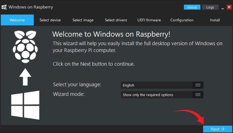
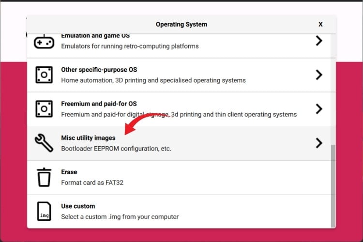
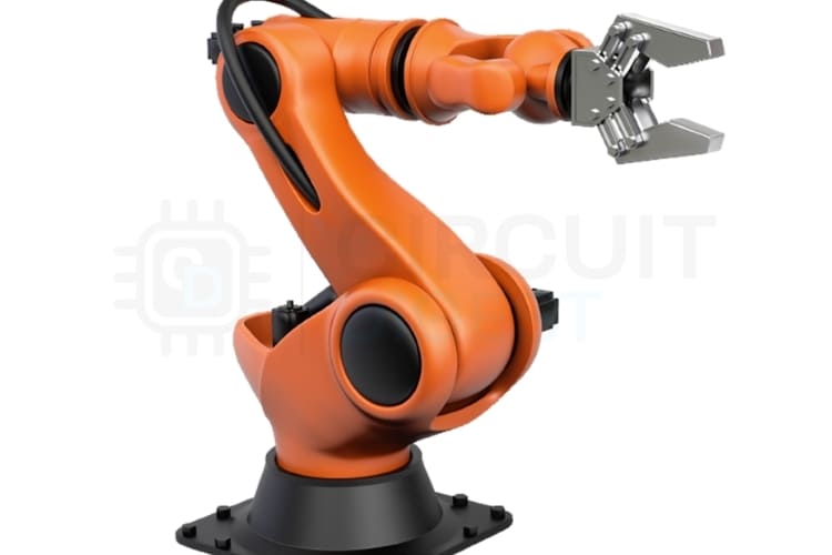
A robotic arm is one of those classic projects that almost every electronics enthusiast tries at some point. It’s a perfect mix of mechanics, electronics, and hands-on creativity and building one teaches you more than any textbook ever could. When most people think of robotic arms, they picture the big, ultra-precise industrial robotic arm machines found in factories or the sleek robots we see in movies like Iron Man(Dummy). Those are exciting to look at, but far too complex for someone who just wants to learn and experiment.
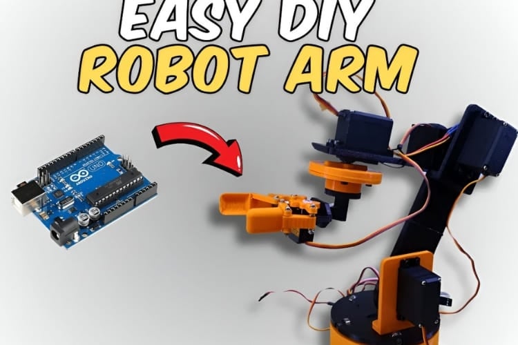
In this article, we’re keeping things simple and practical on beginner-friendly open source robotic arms that you can actually build at home. Instead of industrial-grade robots, we’re focusing on beginner-friendly robotic arm designs that you can actually build at home. No heavy components, no expensive hardware, and no advanced engineering background required. Every simple robotic arm project featured here is open-source, easy to understand, and designed for newcomers who want to learn the basics of robotic movement, servo control, and simple automation.
Whether you're looking for a simple robotic arm using Arduino, a complete 6-axis robotic arm, or a functional pick and place robotic arm, this list covers a wide range of designs that help you understand everything from basic servo control to multi-axis movement. All robotic arm projects include complete robotic arm 3D models, source code, and assembly instructions. If you are more interested in Robotics, do check these Robotic Projects.
What is a Robotic Arm? Understanding the Fundamentals
A robotic arm is a mechanical device which is designed to replicate the movements and functions of the human arm. It is designed to perform tasks with precision, reproducibility, and, in many situations, complete programmable control. Most robotic arms are made up of many stiff parts joined by joints, allowing the robotic arm to move in different directions with a degree of freedom(DOF). The more degrees of freedom an arm has, the more adaptable and capable it is.
Industrial robotic arms exist in a variety of fields. In factories, workers assemble cars, weld metal, pick and arrange components, and paint surfaces with perfect consistency. In medicine, they help the surgeons in operations where accuracy and steadiness play a major role. They are also widely used in laboratories, space missions, and educational settings. At the core, all robotic arm for beginners projects rely on a few key components:
Core Components of Every Robotic Arm
At the core, a robotic arm with a servo motor relies on essential components in Open Source Robotic Arms:
- Actuators - servos or motors that control the movement.
- Controller - the brain of the system, which processes the data, controls the other components, etc…
- End-effector - the tool that is attached at the end of the arm, which is known as a gripper, camera, or scalpel, depending on the process of the project.
Together, these parts allow a robotic arm to interact with its environment in a controlled and purposeful way. Whether it’s lifting small objects, performing surgical procedures, or assembling complex products, the flexibility of robotic arms makes them one of the most powerful tools in modern technology.
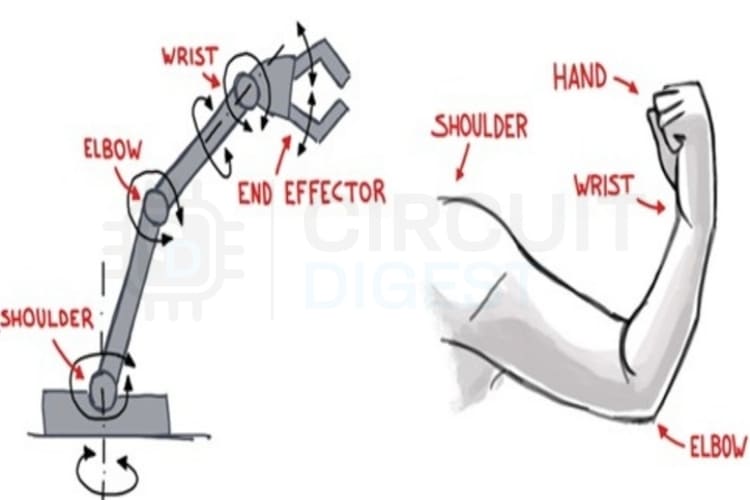
This image compares a robotic arm to a human arm, showing how each joint-shoulder, elbow, wrist, and hand is designed to mimic human movement. It highlights the similarities in structure and function between the two
How We Selected These Open Source Robotic Arm Projects
To make this simple and easy to build, several criteria need to be focused on; they are
- Open-source files availability (STLs, code, schematics)
- Beginner-friendly assembly
- Affordable parts
To ensure these robotic arm projects are genuinely beginner-friendly and practical for learning, we evaluated each design against specific criteria that matter most to newcomers building their first DIY 3D printed robot arm:
Selection Criteria | Why It Matters | What We Look For |
Open-Source Files | Complete STL files, code, and schematics eliminate guesswork | Full 3D models, Arduino/C code, wiring diagrams, BOM |
Beginner Assembly | Simple tools and clear instructions reduce barriers to entry | Basic screwdriver assembly, no CNC/welding required |
Affordable Parts | Budget-friendly components make projects accessible to everyone | Hobby servos (SG90, MG995), common Arduino boards, 3D printed parts |
Clear Documentation | Step-by-step guides ensure successful builds | Assembly videos, detailed tutorials and troubleshooting tips |
1. Open-Source Files Availability (STL Models, Code, Schematics)
Beginners struggle with mechanical design, motor control, and basic kinematics knowledge. Open-source robotic arm, schematics, and source code make the learning process easier by giving complete, ready-to-use resources, which are very helpful for the initial setup. All robotic arms in this article provide fully accessible open-source files to help you start confidently.
2. Beginner-Friendly Assembly Process
Even with the open-source design files, building a DIY 3D-printed robot arm on your own can be a tough task without the proper tools. It's important to choose the designs that can be assembled easily with the help of simple tools. This ensures the beginners can build their own robotic arm DIY project without the need for any advanced tools.
3. Affordable and Accessible Components
Some robotic arms require costly components, making them difficult for beginners to try. Designs that use budget-friendly, easily available parts like hobby servos, 3D-printed pieces, and basic electronics keep the simple robotic arm projects affordable and beginner-friendly.
Essential Terms Every Robotic Arm Builder Must Understand
Before diving into the robotic arm projects, it's crucial to understand the fundamental concepts that apply to every robotic arm design.
1. Joints - The Foundation of Movement
Joints are the moving links in a robotic arm. They let the arm bend, rotate, or change direction, similar to how our elbows and wrists work. In a 6-axis robot arm project, six independent joints work together to achieve complex spatial positioning.
2. Degrees of Freedom (DOF) - Measuring Movement Capability
Degrees of freedom describe how many independent motions a robotic arm can make. Understanding DOF is essential when selecting a robotic arm for beginners:
For example:
1 DOF means the arm moves in just one direction.
3 DOF means it can move up and down, side to side, and also rotate.
The higher the DOF, the more flexible and capable the arm becomes.
3. End-Effector - The Working Tool
The end-effector is the tool attached to the tip of the robotic arm. It could be a gripper, a suction cup, a pen, a welding tool, or anything the arm needs to use to perform a task.
4. Servo Motor Fundamentals - Powering Precision Movement
A robotic arm with a servo motor achieves precise positioning through these electromechanical devices. They rotate to specific angles based on the signals they receive. A robotic arm with a servo motor achieves precise positioning through these electromechanical devices.
A few key points:
- They can only rotate within a set angle range (like 0-180°).
- They provide precise position control.
- Their torque determines how much weight the arm can lift.
If you find it difficult to understand how a servo motor works, our tutorial on How to Control a Servo Motor Using Arduino will guide you step-by-step and make the concept much easier to follow.
5. 3D Design and Modelling for Robot Arms
3D design is the process of creating the arm’s parts in CAD software such as Fusion 360 or SolidWorks. These robotic arm 3D models are later 3D-printed or machined. Good 3D design ensures the parts fit well, move smoothly, and are strong enough for the job. Most open source robotic arms also provide complete robotic arm 3D models, which include STL files, assembly diagrams, and joint layouts that beginners can follow easily while printing or modifying the design.
6. Number of Axes - Movement Dimensions
Axes describe the different directions in which the arm can move.
For example:
- A 2-axis arm can move in only two directions.
- A 4-axis arm has more reach and versatility.
- A 6-axis arm offers very smooth and complex movement, similar to industrial robots.
7. Rotation Limits and Range of Motion
Every servo or joint has a maximum angle it can turn. Many hobby servos rotate up to 180°, while some specialised servos or mechanical joints can rotate a full 360°. These physical limits define workspace boundaries and influence arm design for robotic arm DIY projects.
8. Payload Capacity - Weight Handling Capability
Payload is the maximum weight the robotic arm can safely lift and hold. It depends on factors like the servo’s torque, the length of the arm, and the strength of the materials used. If the payload is too high, the arm may wobble, bend, or cause the motors to stall. Exceeding payload capacity causes motor stalling, joint bending, structural failure, or erratic movement in your DIY 3D printed robot arm.
9. Power Supply Requirements - Critical Electrical Considerations
Robotic arm projects with multiple servo motors, especially those using multiple servos, need a stable and sufficient power source.
Beginners often forget that:
- USB power is not enough
- Servos need separate power
- Current rating (amps) matters as much as voltage
- A weak power supply causes shaking, overheating, or servo failure.
A quality 5V/5A power supply prevents these issues in multi-servo simple robotic arm projects.
10. Control System Selection - Choosing the Right Brain
The microcontroller selection determines your robotic arm for beginners' capabilities and expansion potential:
- Arduino for simple pick-and-place
- Raspberry Pi for advanced control
- ESP32 for wireless control
- Choosing the right controller prevents limitations later.
Top 10 Open Source Robotic Arm Projects for Beginners
Each robotic arm project listed below includes complete build files, source code, and ready-to-use robotic arm 3D models, making it easier for beginners to assemble and understand the mechanical structure. All projects are thoroughly tested, documented, and proven to work for newcomers to robotic arm DIY projects. Let's dive in
1. Object Following Robotic Arm - AI-Powered Tracking System
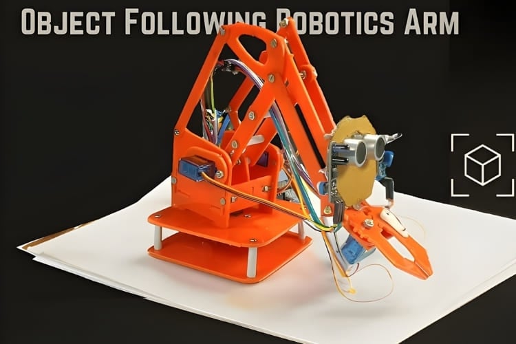
This simple robotic arm project helps you build a 4DOF robotic arm using Arduino UNO controlled by an Arduino UNO controller that can track moving objects. The arm uses four SG90 servo motors managed by a PCA9685 PWM driver, while an ultrasonic sensor and two IR sensors detect object movement. As the object moves, the arm automatically adjusts its position, moving right, left, down or up. The Arduino code includes libraries for precise servo control and sensor reading, making the setup both interactive and responsive. With affordable, modular hardware, this project is an excellent hands-on introduction to robotics, automation, and Object-tracking systems for beginners and hobbyists.
Project Source: Arduino Project Hub (roboattic_lab).
Original Project Link: https://projecthub.arduino.cc/roboattic_lab/build-your-own-object-tracking-4-dof-robotics-arm-with-arduino-dd36ba
2. Robotic Arm using ARM7-LPC2148 Microcontroller - Embedded Systems Learning
This robotic arm DIY project uses the LPC2148-based robotic arm design project, which is based on a simple concept: using four potentiometers to directly control the four joints of a lightweight pick-and-place arm. Each joint is powered by an SG90 servo, and the microcontroller reads the position of the potentiometers through its analog-to-digital converter pins. As you turn a knob, the matching servo moves to the new angle, allowing the arm to respond in real time. The joints include base rotation, vertical lifting, forward reach, and a small gripper, which offers enough flexibility for basic object handling. A set of indicator LEDs shows which motor is currently active. The servos are connected to a separate 5 V power supply to ensure system stability, while the microcontroller operates on 3.3 V. The firmware is written in Keil and uploaded using Flash Magic, making direct use of the chip’s ADC, GPIO, and PWM features. Overall, it’s a clean and practical way to get started with embedded robotics, demonstrating how an ARM microcontroller can be used to control a multi-axis robotic arm using simple analog inputs. The project implements a straightforward yet effective control scheme: four potentiometers directly control four joints of a lightweight pick-and-place robotic arm. The four-joint configuration includes base rotation (360° workspace), vertical shoulder lift, forward elbow reach, and a functional robotic arm gripper—offering sufficient flexibility for basic object manipulation tasks and pick-and-place operations.
Project Source: Circuit Digest-LPC2148 Robotic Arm Project. The 3D printed Robotic Arm used in this tutorial was made by following the design given by EEZYbotARM, which is available on Thingiverse.
Project Link: https://circuitdigest.com/microcontroller-projects/diy-robotic-arm-using-lpc2148-microcontroller
3. Dolphin 3D-Printed Robotic Arm - Smooth Articulation Design
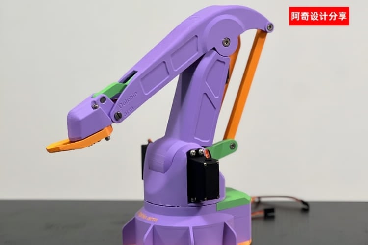
The Dolphin Robotic Arm is a smoothly designed, DIY 3D printed robot arm project made for makers looking for a simple yet functional robotic arm. Its design emphasises stability and smooth movement, with several rotating joints that let it perform basic pick-and-place tasks. The parts are easy to print and put together, and the creator offers all the necessary files, a list of materials, and step-by-step instructions, making it easy for even new builders to follow. The arm uses common hobby servos, which means the electronics are affordable and simple to control using an Arduino or similar microcontroller. As a whole, it's a small, user-friendly robotic arm that helps beginners learn about joint movement, servo control, and the fundamentals of pick-and-place robotic arm systems. Feature optimised robotic arm 3D model files for standard FDM printers (0.2mm layer height). This project serves as an excellent entry point for beginners who want to understand joint kinematics, servo motor control fundamentals, and the mechanical principles that govern simple robotic arm projects.
Project Source: MakerWorld – Dolphin Robotic Arm Model.
Original File Link: https://makerworld.com/en/models/91498-dolphin-arm-robotic-arm
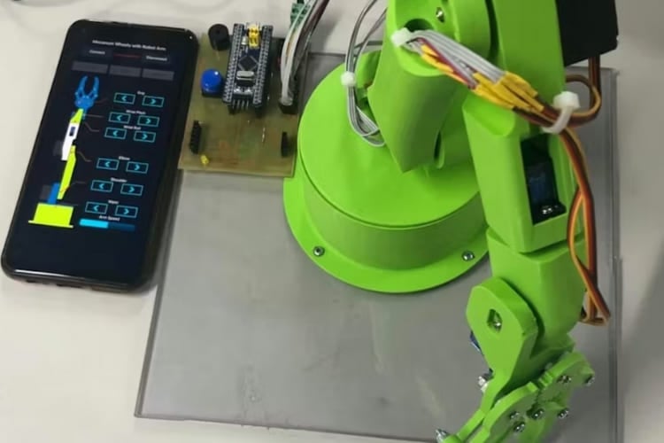
4. ESP32 Robot Arm with Smartphone Control - Wireless Web Interface
A robotic arm with a servo motor achieves precise positioning through these electromechanical devices. Key specifications include:
This modern robotic arm project, using an Arduino-compatible ESP32 platform, demonstrates wireless control capabilities through an intuitive web-based interface. The ESP32 runs a web-based interface where users can adjust each joint base, elbow, shoulder and robotic arm gripper using sliders on the screen. As you move the sliders, the servos which are present respond instantly, allowing for real-time adjustments. The system can also include record and playback functions, enabling you to save a sequence of movements and replay them later when needed. The frame is lightweight and can easily be constructed using 3D printing, making it easy to assemble each and every part, which is ideal for beginners who want to explore the servo control, wireless communication and web-based robotics. As you move the on-screen sliders, the servo motors respond instantly with minimal latency, enabling real-time adjustments and smooth coordinated motion. Features a lightweight DIY 3D printed robot arm frame optimised for servo torque. This is an ideal project for beginners interested in exploring wireless robotics, web-based control interfaces, and IoT (Internet of Things) integration with robotic arm designs.
Project Source: YouTube Creator (Channel Name: hash include electronics).
Original Video Link: https://www.youtube.com/watch?v=cVSvg6VQhGU
5. 3D-Printed 6-DOF Arduino Robotic Arm - Advanced Multi-Axis Control
This comprehensive 6-axis robot arm project features a complete 6-axis robotic arm design with full spatial positioning capability, enabling it to move naturally and perform complex manipulation tasks similar to human arm capabilities.
This is a complete 3D-printed robotic arm with six degrees of freedom (DOF), allowing it to move flexibly and naturally, similar to a human arm. The project uses an Arduino UNO as its main control board, which sends signals to several servo motors to control the movement of each joint. Because of these six degrees of freedom, the arm can move in many different directions, giving it the ability to do complex tasks, not just simple ones like picking up and placing objects. The whole structure is made from 3D-printed parts, making it inexpensive and easy to build for people who are just starting out. The design is also modular, meaning each joint is separate and controlled by its own servo motor. This makes putting it together much easier, and you don't need any specific tools or machines to assemble it. These robotic arm 3D models are exported as STL files for 3D printing or used to generate machining instructions. Most open-source projects provide complete robotic arm 3D models, including STL files, assembly diagrams, and detailed joint layouts that beginners can follow while printing or modifying the design for custom applications. This configuration enables the arm to reach any point within its workspace while maintaining complete control over tool orientation, capabilities typically found only in professional industrial robotic arms. This robotic arm for beginners project teaches advanced concepts while remaining achievable for dedicated hobbyists.
Project Source: YouTube Creator (Channel Name: Oliver Paff)
Original Video Link: https://www.youtube.com/watch?v=n8HHMt3xdFA
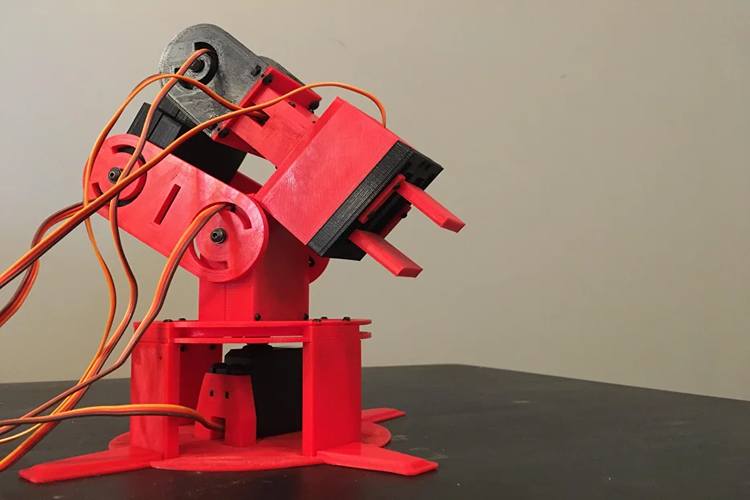
6. DIY 6-DOF Robot Arm with Arduino - Production-Grade Design
This project features a 6-axis robot arm project, which is built from 3D-printed components and controlled by an Arduino. With six independent axes of motion, the arm can perform complex manipulation tasks, not just simple pick and place tasks. Each joint (base, shoulder, elbow, wrist, and gripper) is controlled by a servo or similar actuator, giving it a wide range of motion. The design is compact and also strong, and the use of 3D-printed parts makes it affordable and accessible for beginners and learners. The Arduino controller sends PWM signals to each motor, enabling precise and coordinated movement across all joints. The open-source nature of the design (with publicly shared STL files and code) makes it ideal for anyone who wants to build, modify, or extend the arm for their own robotics experiments. This configuration mirrors the joint structure found in professional industrial robotic arms used in manufacturing automation. The characteristic reinforced DIY 3D printed robot arm structure handles a moderate payload (200-300g).
Project Source: YouTube Creator (Channel Name: Lee Curiosity).
Original Video Link: https://www.youtube.com/watch?v=bNzVCNyYDzM
7. STM32 Robot Arm With Smartphone Control - Professional Embedded Design
This advanced robotic arm DIY project features a 6-DOF robotic arm design powered by a mix of MG995 and SG90 servo motors. It uses an STM32F103 (Blue Pill) as the main controller, while an ESP32 handles Bluetooth communication with a simple MIT App Inventor-based smartphone app. Commands sent from the smartphone are passed to the STM32, which drives each servo using precise PWM control. The design includes a custom PCB, stable power regulation, and complete build files, making it a practical and well-documented project for anyone who wants to explore embedded side and wireless robotics. The system represents a step up from basic robotic arm using Arduino projects, demonstrating embedded systems design practices used in commercial robotics products.
Project Source: Hackster.io - Labirenti Project Page.
Original Project Link: https://www.hackster.io/Labirenti/stm32-robot-arm-with-smartphone-control-92955b
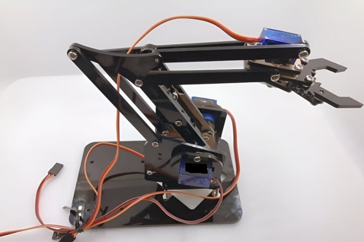
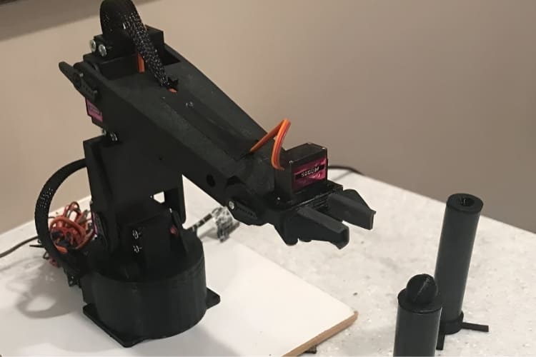
8. DIY Robotic Arm - Simple Yet Functional Design
This straightforward, simple robotic arm project uses 3D printing and regular servos for each joint, keeping costs low and assembly simple. This do-it-yourself robotic arm design is made using 3D printing and uses regular servos for each joint, which keeps the cost low and makes it simple to build. The design includes printable parts for the base, rotating platform, arm sections, and a robotic arm gripper, all of which fit together using basic screws. The arm can move in multiple directions, making it good for simple pick-and-place activities. Its easy setup is perfect for people who are new to building robots. The project comes with full STL files and detailed instructions, so anyone can print the parts, attach the servos, and get the arm up and running without needing special tools. The straightforward mechanical design and simple servo control make this an ideal first project for newcomers who want hands-on experience with robotic arm 3D models, basic kinematics, and servo programming without getting overwhelmed by complex control algorithms or difficult assembly procedures.
Project Source: Printables - DIY Robotic Arm Model.
Original File Link: https://www.printables.com/model/41837-diy-robot-arm
9. Simple 3D-Printed Servo Robotic Arm - Practical Learning Platform
This completely 3D-printed robotic arm for beginners is a great project for beginners and has real-world use. It uses SG90 and MG995 servos, which provide enough power for simple pick-and-place activities. All the parts are made using a 3D printer and can be put together easily with just basic screws-no special tools are required. The arm is controlled by an Arduino, allowing for smooth movement based on angles. It also comes with STL files and wiring instructions. This project is perfect for those who want to learn about mechanical design, servo control, and multi-axis motion without spending a lot of money. It strategically employs a combination of SG90 servos (lightweight, low-cost) and MG995 servos (higher torque, metal gears) positioned according to load requirements—demonstrating proper servo selection principles that apply to all robotic arm projects.
Project Source: YouTube Creator (Channel Name: Emre Kalem).
Original Video Link: https://www.youtube.com/watch?v=CHV36hu9z3E
10. 3D Printed Arduino-Based Robotic Arm by BasementMaker
The BasementMaker DIY 3D printed robot arm is a completely open-source project that brings together 3D-printed components with an Arduino Mega and regular hobby servos to make a smooth and dependable six-axis robotic arm. It was designed after several improvements to enhance its strength and movement performance. The arm includes a strong printed base, several rotating joints, and a working robotic arm gripper, which makes it perfect for simple pick-and-place tasks. All the STL and STEP design files are available for free, along with detailed step-by-step guides for printing, building, connecting the electronics, and programming. It's perfect for serious beginners ready to tackle a comprehensive 6-axis robot arm project with professional-grade documentation.
Project Source: Instructables-3D-Printed Arduino-Based Robotic Arm
File Link:https://www.instructables.com/3D-Printed-Arduino-Based-Robotic-Arm/
If you’re interested in a mobile version of a pick-and-place system, you can also explore our Bluetooth-Controlled Pick and Place Robotic Arm Car project
Comprehensive Comparison: Top 10 Robotic Arm Projects
The table below summarises the key features of all 10 open source robotic arms projects covered in this article, making it easier to compare their controllers, DOF, build type, & suitability, etc.
| S.NO | Project Name | Controller
Used | DOF | Built-Type | Motor | Control Method | Suitable For |
| 1 | Object Following Robotic Arm | Arduino UNO R3 | 4 DOF | 3D-printed | SG90 Servo Motors | Arduino
-based sensor control | Object tracking, basic automation,learning robotics. |
| 2 | Robotic Arm using LPC2148 | ARM7 LPC2148 | 4 DOF | Lightweight mechanical build | SG90 servos | Potentiometer manual control | Learning ADC, PWM, embedded control |
| 3 | Dolphin 3D-Printed Robotic Arm | Arduino/Similar | 4 DOF | Fully 3D printed | Standard hobby servos | Basic Arduino control | New makers wanting simple, stable motion |
| 4 | ESP32 Smartphone/Web-Controlled 4-DOF Arm | ESP32 | 4 DOF | Lightweight, likely 3D-printed | Hobby servos | Web UI sliders + Record/Play | Wireless control learning |
| 5 | 3D-Printed 6-DOF Arduino Arm | Arduino UNO | 6 DOF | Fully 3D printed | Multiple servo motors | Arduino angle control | Intermediate users wanting complex motion |
| 6 | DIY 6-DOF Arduino Robot Arm | Arduino UNO | 6 DOF | 3D-printed | Mixed servos | Arduino PWM | Advanced hobby projects & experiments |
| 7 | STM32 Robot Arm with Smartphone Control | STM32F103+ESP32 | 6 DOF | Mixed 3D-printed + custom PCB | MG995 + SG90 | Smartphone App (Bluetooth) | Embedded systems learners |
| 8 | DIY Robotic Arm (Printables) | Arduino UNO/Similar | 5 DOF | Fully 3D-printed | Hobby servos | Basic servo control | Beginners with 3D printers |
| 9 | Simple 3D-Printed Servo Arm | Arduino UNO | 5 DOF | Fully 3D printed | SG90 + MG995 | Wired Arduino control | Mechanical design & servo basics |
| 10 | 3D Printed Arduino Based Robotic Arm | Arduino Mega | 6 DOF | Fully 3D-printed | Mix of hobby servos: MG996R / MG90S / SG90 / SG5010 | Button-based manual control using Arduino Servo library | Beginners learning robotics, servo control, and 3D-printing projects |
Real-World Applications of Robotic Arms
Understanding where robotic arm designs are deployed in industry and research helps contextualise your learning and reveals potential career paths in robotics engineering and automation technology.
- Industrial Automation:
The robotic arms are widely used in welding, painting, packaging, and assembling products. Industrial robotic arms form the backbone of modern manufacturing facilities, performing repetitive tasks with precision, speed, and consistency that human workers cannot match. - Medical and Surgical Assistance:
These will assist in precise surgical procedures, rehabilitation, and handling delicate medical tasks that require stability and accuracy. Specialised 6-axis robotic arms assist surgeons in minimally invasive procedures requiring extreme precision and stability. - Laboratory Automation:
Robotic arms can able to handle the test tubes, samples and looped lab tasks, which also helps in reducing human error. Pick and place robotic arms automate repetitive laboratory tasks: pipetting samples, handling test tubes, preparing microtiter plates, organising specimens, and executing standardised protocols. - 3D Printing and Fabrication:
Advanced arms are used in additive manufacturing, printing large or complex components with precision. Advanced robotic arms enable large-scale additive manufacturing by printing complex components layer by layer. - Agriculture:
They help in sorting, planting, harvesting, reducing the labour cost and improving the overall efficiency. Specialised robotic arm grippers adapted for delicate produce enable automated harvesting, sorting, planting, and packaging operations. - Hazardous Environment Operations:
Robotic arms can perform tasks in dangerous environments, such as handling chemicals, explosives, or radioactive materials, keeping humans safe. Remote-controlled industrial robotic arms perform dangerous tasks in environments hostile to human workers. - Education and Research:
They are excellent tools for learning robotics, automation, and programming, giving hands-on experience with real-world applications. Affordable robotic arms using Arduino and 3d printed robot arms serve as excellent educational tools, providing hands-on experience with robotics principles, automation fundamentals, programming concepts, and engineering problem-solving. - Food Industry:
Used for sorting, packaging, and handling food items in hygienic conditions, improving speed and reducing contamination. Food-safe robotic arm designs automate sorting, packaging, decorating, and assembly of food items in hygienic conditions.
Frequently Asked Questions About Robotic Arm Projects
⇥ 1. Are all these robotic arm projects open-source?
Yes, every project which is listed here is Open-Source and you can able to download code,3D design files, etc..all for free.
⇥ 2. Do I need a strong background in robotics to build these arms?
No. Most of the projects are designed with beginners. If you follow the steps carefully, you can also build a fully working robotic arm with the basic knowledge of servos, microcontroller and simple mechanical knowledge.
⇥ 3. What kind of materials are used to build these robotic arms?
Many of the Robotic arms use the 3D-printed parts with the servos. Some of the arms use Acrylic sheets or ready-made brackets.
⇥ 4 . Which microcontrollers are often used in these projects?
The common controllers which are all used in the above robotic arms are Arduino UNO, Arduino Mega, ESP32, NodeMCU, STM32, etc.
⇥ 5. How many degrees of freedom do these robotic arms have?
Most beginner-level arms range from 3 to 6 DOF. More DOF means the arm can move more freely, but it also requires more motors and wiring.
⇥ 6. Can I build these arms without a 3D printer?
Yes. Some projects use acrylic or standard servo brackets that don’t require any printing. But having access to a 3D printer makes the build easier and lets you customise parts.
⇥ 7. What basic tools do I need to assemble a robotic arm?
A Set of screwdrivers, a small soldering iron, and, in some cases, a 3D printer to make the 3D models. Mostly, the listed Robotic Arms don't need any special tools.
Conclusion For the Top 10 Robotic Arms
Open source robotic arm designs make it easy for anyone to explore robotics without needing advanced experience or expensive tools. With ready-to-use robotic arm 3D models, schematics, and code, beginners can understand how joints, servos, and different control systems work by actually building and experimenting. Explore wireless ESP32 connectivity, or master multi-axis coordination with a complete 6-axis robot arm project. The robotic arm projects listed in this article offer a solid starting point, whether you want to learn basic movement of a pick and place robotic arm, practice 3D printing, or explore multi-axis control. These robotic arms, using Arduino and similar microcontrollers, not only teach fundamental concepts but also encourage experimentation, modification, and innovation. The DIY 3D printed robot arm that is mentioned will not only encourage you to learn, but it will also help you to improve and create your own design. If you're interested in how robotic arm designs are being used in real industrial applications, you can also explore our interview on STMicroelectronics’ STM32MP2 AI Robot Demo at Electronica India 2025. Every industrial robotic arm engineer started somewhere, and these beginner-friendly robotic arm DIY projects provide the perfect foundation for your robotics journey.
Previously, we have built many interesting projects on a robotic arm. If you want to know more about those topics, links are given below.
Robotic Arm Control using PIC Microcontroller
Control a multi-servo robotic arm using the PIC16F877A microcontroller by generating PWM signals on GPIO pins, reading potentiometer inputs, and driving servos with timer interrupts in a hands-on embedded systems project.
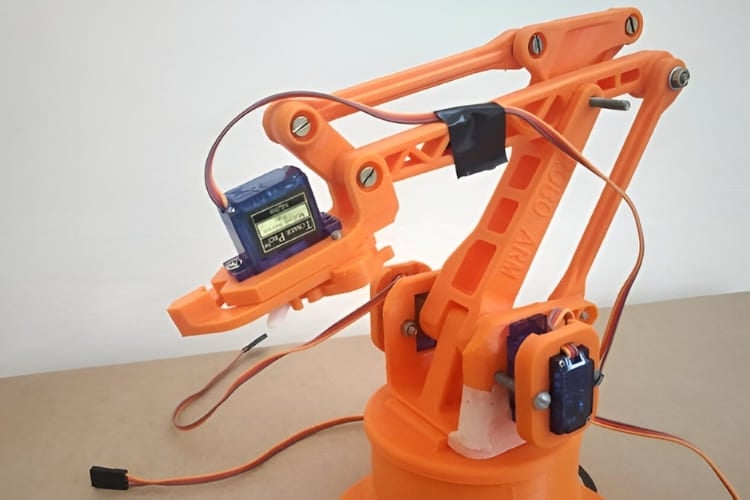
How to build a Simple Arduino Robotic Arm
In this tutorial, we design an Arduino Uno Robotic Arm. This Robotic Arm can be controlled by four Potentiometers attached to it, each one used to control a servo motor.