STMicroelectronics showcased what their STM32MP2 microprocessors are capable of at their electronica India 2025 booth. Visitors could play a game of tic-tac-toe with a robotic arm. The demonstration clearly exhibited how the chips allow for AI-powered robotic applications without cloud connectivity.
You’re hunting through component distributors trying to find that perfect microcontroller for your project. Let’s say you need three SPI controllers, I²C interfaces, and some specific ADC configuration. You go on to find something that has just the right number of SPI controllers, but before you celebrate, you notice it lacks I²C compatibility.
ROHM Semiconductor was among the key players that exhibited at electronica India 2025. The company’s Group Manager - Technical Centre, Balaji Karthic, while giving us an overview, called attention to their near two decades of research and development in SiC (silicon carbide) that led to their fifth-generation devices.
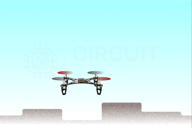
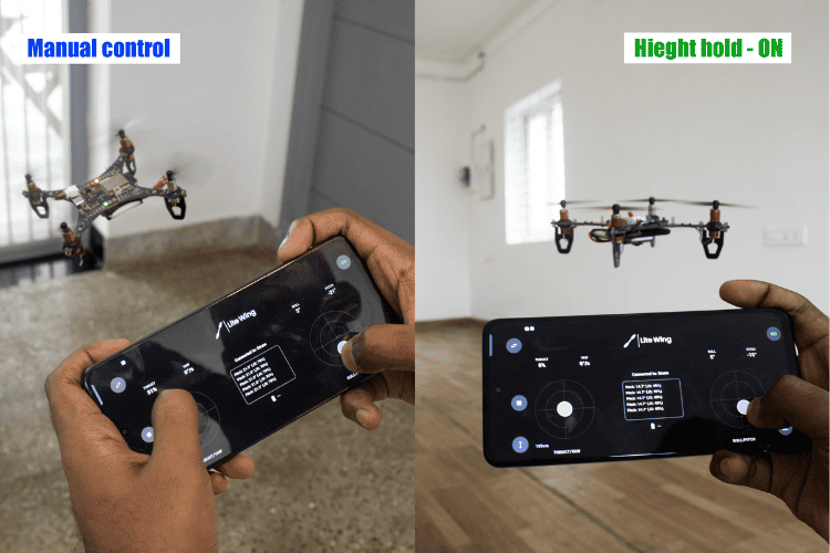
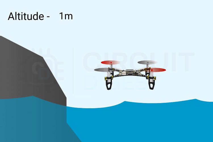
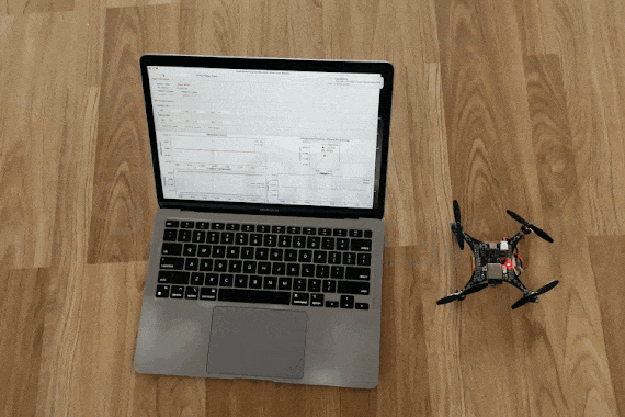
Flying a drone manually requires constant attention to throttle control. One moment of distraction and your drone either crashes into the ground or flies away into the ceiling. If you're building your LiteWing from scratch, check out our detailed step-by-step LiteWing assembly guide to get started with your build. This is where Drone height hold mode becomes a game-changer for drone pilots of all skill levels. Height hold drone automatically maintains your drone at a specific height, letting you focus on horizontal movement while the flight controller handles the vertical stability.
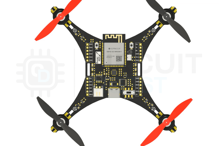
The LiteWing drone, an open-source ESP32-powered drone that evolved from our popular DIY WiFi-controlled drone project, makes implementing altitude hold mode drone surprisingly straightforward. Unlike expensive commercial drones that come with this feature built in, height hold mode in LiteWing allows you to understand and build this functionality yourself. In this tutorial, we'll walk you through adding height hold capability to your LiteWing using the VL53L1X Time-of-Flight (ToF) sensor using both the cfclient software and our updated LiteWing mobile App. The LiteWing includes dedicated solder pads on the bottom side of the PCB frame to attach the off-the-shelf VL53L1X module directly.
This laser-ranging sensor provides millimetre-accurate distance measurements up to 4 meters, making it perfect for indoor flight applications and precise altitude control drone operations. The VL53L1X communicates over I2C and integrates seamlessly with LiteWing's existing flight control firmware. Once connected, the sensor continuously measures the distance to the ground, and the flight controller uses this data to adjust motor speeds and maintain your desired height automatically.
Height hold mode will convert your drone from being operated manually on your behalf to an autonomous height-holding platform. This mode uses multiple sensors along with advanced algorithms to hold a set height without input from the user, which is necessary for reliable operations.
The Significance of Height Hold:
Hands-free hover: Can maintain an altitude and gives the operator the ability to concentrate on video capture or avoiding obstacles.
Decreased workload: Relieves the pilot from frequent throttle control, particularly important for less experienced pilots.
More time in the air: Allows for optimal performance of the motors to gain more time in the air by not using unnecessary power to gain or lose height.
Increased safety: Prevents unintended loss of controlled altitude that could cause a crash or fly-away.
Better Aerial Photography: A stable platform allows for smoother video and pictures, and will produce higher quality.
Increased accuracy: A must for indoor pilots and for inspection work and confined spaces.
How Height Hold Mode Works
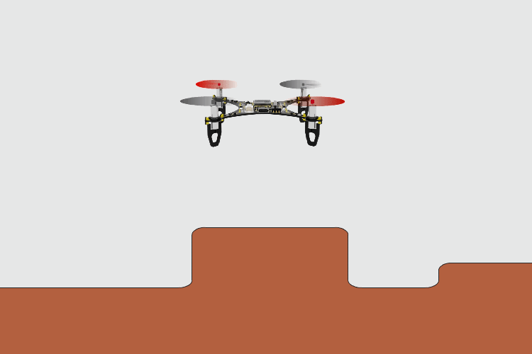
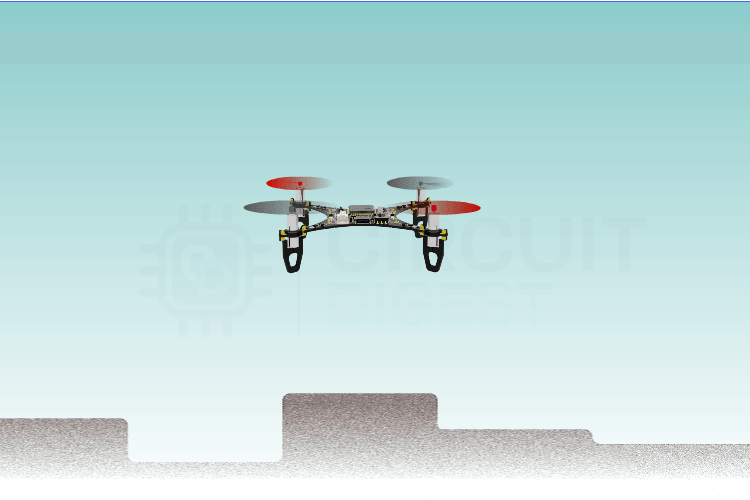
Height hold in drone mode transforms your drone from a manually controlled aircraft into an autonomous hovering platform. This advanced altitude control drone uses multiple sensors and sophisticated algorithms to maintain a constant height without pilot intervention.
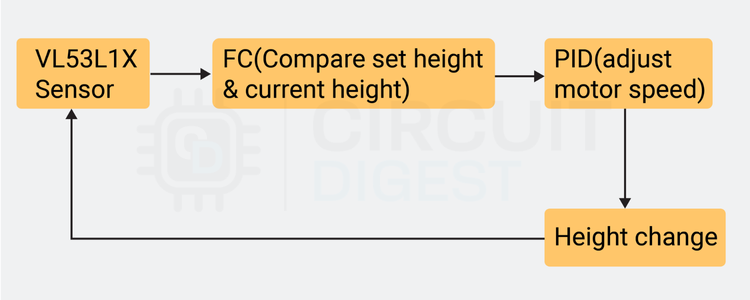
Drone's height hold operates as a closed-loop feedback control system that continuously compares the drone's actual height with a predetermined target height. When you activate height hold mode, the flight controller captures the current height as the reference point and works to maintain this position regardless of external disturbances.
The height hold in drone systems consists of several interconnected components working in perfect harmony:
Sensor Array: Multiple height measurement devices provide redundant height data
Flight Controller: The central processing unit that interprets sensor data and makes control decisions
PID Controller: A mathematical algorithm that calculates precise motor adjustments
Motor Control System: Electronic speed controllers that modify rotor speeds based on flight controller commands
Feedback Loop: Continuous sensor readings create a responsive system that adapts to changing conditions
Types of Sensors Used for Altitude Control in Drones
Modern altitude hold mode drone systems employ various sensor technologies for height measurement, each with distinct advantages and limitations. Understanding these differences helps you choose the right sensor for your specific altitude control drone application.
Sensor Type
Range
Accuracy
Best For
Limitations
Barometric Pressure
Unlimited altitude
±1-3 meters
Outdoor high-altitude flight
Weather-dependent, measures altitude not ground distance
Ultrasonic
0-8 meters
±2-5 cm
Low-cost indoor applications
Affected by soft surfaces, wind interference
ToF Laser (VL53L1X)
0-4 meters
±1 mm
Precision indoor hovering
Limited range, bright sunlight interference
GPS + Barometer
Unlimited
±2-5 meters
Outdoor navigation, waypoints
No indoor functionality, GPS dependency
Barometric Pressure Sensors for Height Hold
Barometric Pressure Sensors measure atmospheric pressure changes to determine altitude. These sensors work well for maintaining height over large areas, but can be affected by weather changes and air currents. They're particularly useful for outdoor flight at higher altitudes where pressure differences are more pronounced.
Technically, this is altitude hold rather than height hold, since barometric sensors measure altitude above sea level (absolute altitude) rather than distance from the ground below (relative height). A drone using only barometric sensors will maintain the same pressure altitude even if flying over terrain that rises or falls, potentially resulting in varying distances from the ground. For this reason, barometric sensors are often combined with ground-relative sensors like ToF or ultrasonic for comprehensive altitude control drone systems.
Ultrasonic Sensors for Height Hold
Ultrasonic Sensors emit sound waves and measure the time for echoes to return from the ground. While cost-effective and reliable at close range (typically under 8 meters), they can struggle with soft surfaces like grass or carpet that absorb sound waves. Wind can also deflect the sound waves, causing inaccurate readings and affecting drone height hold performance.
Time-of-Flight (ToF) Laser Sensors for Precision Height Hold
Time-of-Flight (ToF) Laser Sensors use infrared laser pulses to measure distance with high precision. These sensors offer excellent accuracy across various surface types and lighting conditions, making them ideal for indoor flight and precise hovering applications. ToF sensors are the preferred choice for height hold mode in LiteWing and similar DIY drone projects.
PID Controller: The Brain Behind Height Hold Mode
The heart of height hold in drone functionality lies in the PID controller algorithm, just as with other flight controller functionalities that utilise PID. This mathematical system doesn't just react to height errors—it predicts and prevents them. The PID controller continuously adjusts motor speeds dozens of times per second to maintain the desired height.
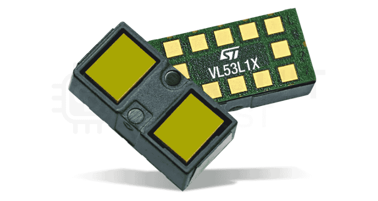
VL53L1X ToF Sensor for Implementing Drone Height Hold
The VL53L1X Time-of-Flight sensor represents cutting-edge technology specifically designed for precise distance measurement in drone measurement in drone height hold applications. This laser-ranging sensor provides the accuracy and reliability essential for effective altitude hold mode drone functionality. The VL53L1X operates using Class 1 laser safety standards, emitting infrared light at a 940nm wavelength.
VL53L1X Technical Specifications for Height Hold
Measurement Range:
4cm to 4 meters with high accuracy
Update Rate:
Up to 50Hz for real-time altitude feedback
Accuracy:
±3% at 1 meter distance under optimal conditions
Field of View:
Narrow 27° cone for precise ground targeting
Supply Voltage:
2.6V to 3.5V operation
Interface:
I2C communication protocol
Current Consumption:
20mA active, 5μA standby
The VL53L1X uses Direct Time-of-Flight measurement, where the sensor emits short infrared laser pulses and measures the precise time required for light to travel to the target and return. Unlike indirect ToF methods that measure phase differences, direct ToF provides absolute distance measurements independent of surface reflectivity variations.
The sensor incorporates a Vertical Cavity Surface Emitting Laser (VCSEL) array and a Single Photon Avalanche Diode (SPAD) detector array. This combination enables the detection of individual photons, allowing measurements even from surfaces with low reflectivity. For optimal flight time with height hold enabled, selecting the right battery is essential, learn more in our comprehensive guide on how to choose the right battery for your LiteWing drone.
Limitations of VL53L1x ToF Sensor
While highly effective, the VL53L1X has operational limitations:
Bright Light Interference: Intense sunlight or bright artificial lighting can saturate the photon detector, reducing accuracy
Maximum Range: A 4-meter limit requires alternative sensors for higher altitude operations
Power Consumption: Active laser operation draws more current than passive sensors
Reflective Surfaces: Highly reflective surfaces may cause measurement errors due to specular reflection
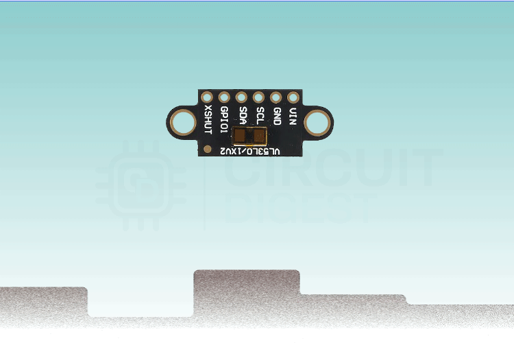
VL53L1X Module
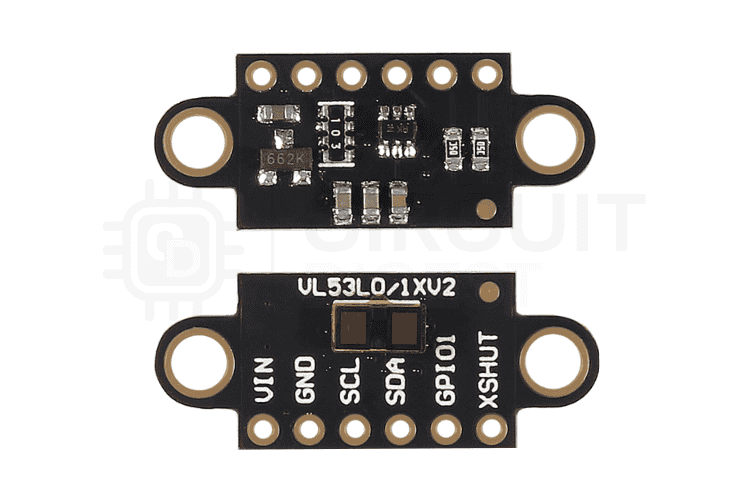
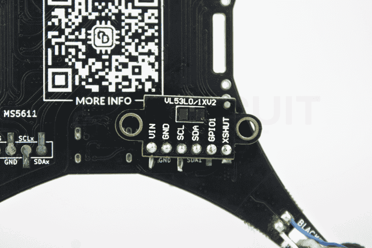
For ease of use, we have used an off-the-shelf VL53L1x module with the LiteWing. We have connected it to the LiteWing drone using SMD male pin headers. Keep in mind that there are different modules with different boards and pin layouts in the market. So, choose the one that looks similar to the one shown in the above picture if you are planning to attach it to the bottom pads of the LiteWing.
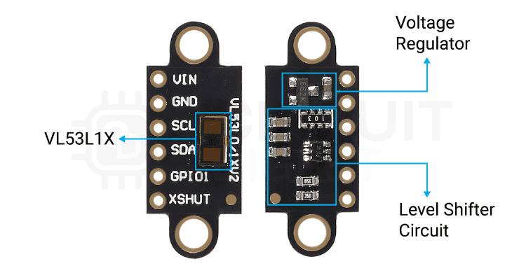
VL53L1X Module Parts Marking
The image below shows the typical component arrangement in a VL53L1x module. As you can see, the module has a bare minimum of components. Apart from the VL53L1x sensor itself, the module has a 3.3V regulator along with level-shifting circuitry and some bypass capacitors. The inbuilt voltage regulator and the level-shifting circuit ensure that the module can be used with either 5V or 3.3V circuits.
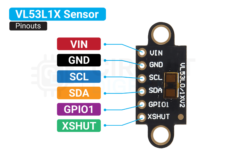
VL53L1X Module Pinout and Connections
Standard breakout modules feature the following pin configuration:
VIN - Positive Voltage Input Pin.
GND - Ground Voltage Input Pin.
SCL - I2C Serial Clock Pin.
SDA - I2C Serial Data Pin.
GPIO1 - Interrupt output.
XSHU - Shutdown Pin, Active Low.
The VIN pin is used to supply power to the module. It typically accepts a regulated input voltage such as 3.3V or 5V, depending on the board design. The GND pin serves as the electrical ground, providing a common reference point for the power supply and signal levels. Communication with the module is achieved via the I2C interface, which uses two pins: SCL for synchronising data transfer, and SDA for sending and receiving data between the sensor and the microcontroller. In addition to these, the module includes a GPIO1 pin, which can be configured as an interrupt output to notify the host system when new ranging data is available or when a specific condition is met. Lastly, the XSHUT pin functions as a hardware shutdown control. It is an active low input, meaning the module enters a low power state when this pin is pulled to ground, and resumes normal operation when driven high.
Installing VL53L1X Sensor for Height Hold Mode in LiteWing
In the LiteWing platform, the VL53L1X connects to the flight controller via the secondary I2C interface, since the primary I2C in LiteWing is used to connect with the IMU onboard. The sensor mounts on the drone's underside with the laser aperture facing downward. You can either use the dedicated pads on the bottom side of the LiteWing or the SDA1 and SCL1 pins available on the GPIO header to interface the VL53L1x sensor module with LiteWing, streamlining the drone height hold setup process.
.
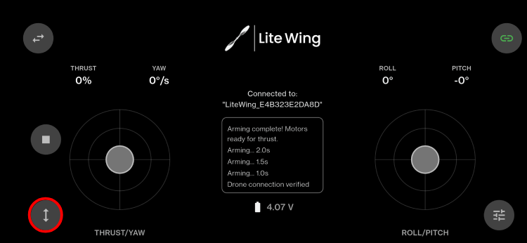
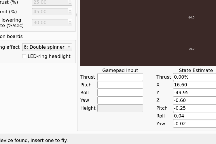
Flying LiteWing in Height Hold Mode
Now that we are familiar with how the drone height hold works, let's look at how to use it. Flying the LiteWing drone is pretty easy. For that, make sure to attach the VL531X sensor module securely to the LiteWing drone. Once done, all you have to do is first install the latest version of the LiteWing App from the Google Play Store or the Apple App Store. To know more details about configuring and using the LiteWing app, please check out our LiteWing app tutorial( hyperlink). Once the app is configured properly, open the app and connect to the drone. Once it's connected, click on the height hold button. Flying the LiteWing with height hold mode in LiteWing activated transforms your piloting experience, making stable hovering as simple as pressing a button.
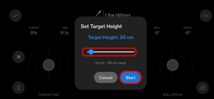
Now, when the set target height option is shown, set your desired height for the drone and click on the start button.
The drone will count down to three and take off on its own. Once the set height is reached, the LiteWing will automatically hold the height and hover at that. Now you can start flying the LiteWing drone by simply using the roll and pitch controls.
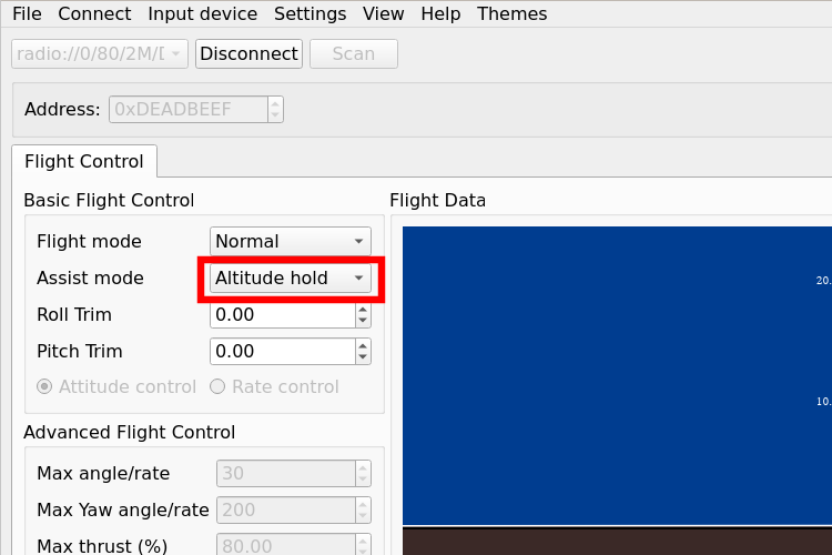
Using cfClient Software for Advanced Height Hold Control
To use the height hold in drone in cfClient, make sure to install and configure the cfClient following the instructions in the How to use Crazyflie cfClient with Litewing tutorial. One thing to keep in mind that to don’t forget to configure the assist control button in the input device configuration. You can also find detailed instructions to do that in the previously linked tutorial. Once everything is configured correctly, turn on the LiteWing drone with the ToF sensor installed and connect to its WiFi. Once the WiFi is connected, connect to the LiteWing using the connect button in the cfClient. Once connected, you can see that the height hold mode in the Assist mode menu is now active.
Now, to use the height hold mode, make sure to select the height hold mode in the Assist mode dropdown menu. You can set your preferred height at which the LiteWing drone needs to be hovering in the gamepad input menu. You can see the default value is around 0.4 meters. Make sure this value is between 0.1 and 3meters for the best result.
Once the desired height is set, press and hold the assist control button in the controller. The drone will automatically take off and hover at the set height. To keep flying the drone, you must keep pressing the assist control button, and to land, just release the button; the drone will reduce the motor speed and land. Here is a demo showcasing the height hold functionality of the LiteWing drone.
FAQ - Height Hold Mode in LiteWing
⇥ 1. Why does the height hold not work with the LiteWing drone? Make sure to attach the VL53L1X sensor module to the drone.
⇥ 2. Even after connecting the ToF sensor, the height hold mode is not working with the LiteWing. Make sure all the connections are correct. And you can check if the sensor is detected or not in the boot log.
⇥ 3. The height hold is working fine indoors, but not outdoors. Why? Since the Vl53L1X sensor is an optical sensor, bright light can affect its functionality. If the outdoors is too sunny, it can affect the sensor. We would recommend using the height hold mode indoors.
⇥ 4. Height hold is working fine with the app, but not with cfclient. Why? In the cfClient, the assist mode must be set to height hold. Also, you should use the assist control button for takeoff.
Other LiteWing Related Projects & Tutorials
Ready to take your LiteWing drone to the next level? Check out these related projects and tutorials that expand your drone's capabilities with gesture control, mobile apps, and advanced flight features.
In this article, we will focus only on Cflib, which is a Python SDK from Crazyflie that allows you to write your own Python code to control your LiteWing drone. If you are not a fan of Python programming, you can also program your LiteWing using Arduino and directly reflash your ESP32, but that is for a different tutorial.
During electronica India and productronica India 2025, CircuitDigest sat down with Kevin Hess, Senior Vice President of Marketing at Mouser. The discussion covered his 35-year career at Mouser, shifts in electronics marketing, and the company’s outlook for India. The veteran reflected on the days of catalog-based sales and how he witnessed it transform into the current digital era.
Power Integrations displayed a wide array of new tech for applications including EVs, railways, industrial power supplies, and renewable energy systems at electronica 2025. In their booth, we met with Andrew Smith, their Director of Technical Outreach and Director of Training, who walked us through some of the key highlights. The company showcased its range of switch technologies featuring integrated switcher ICs with voltage ratings of 750 V, 900 V, 1250 V, and 1700 V. Smith underscored, "This makes our integrated switcher ICs very good for the Indian environment."
The company uses three semiconductor materials in their switches: silicon, gallium nitride (referred to as "PowiGaN"), and silicon carbide. The GaN tech is their in-house replacement for traditional MOSFETs in their flyback switcher ICs. Engineers can use the same converter IC with different switch tech on the inside, making it far less of a challenge to select the best tech for their needs. "Our aim is to make it very easy for the engineer to use whichever of those technologies they would like to explore by using the same converter IC with a different switch inside," said Smith.
He pointed out to us a 70-watt design of a bridge switch inverter driver board that was accompanied by support software. The software served as a virtual oscilloscope and offered performance monitoring by capturing characteristics of a motor. The demo used a single-output motor. He emphasized the minimal power consumption quality of the company’s bridge switch technology in standby mode. A 150-watt motor on display used as little as 8 milliwatts.
The company also showcased LLC half-bridge designs for EV and tool chargers, featuring a 720-watt design with programmable current charging for applications including two-wheeler chargers, using their HiperLCS-2 family and Power Factor Controller ICs. Additionally, they demonstrated their gate driver technology portfolio, including fully integrated three-level gate driver architectures and dedicated gate driver boards for power modules across alternative energy, thermal, and automotive applications.
From the company’s press release, the RDK-85SLR is their reference design kit for solar-powered race cars targeted at student teams to compete in the Bridgestone World Solar Challenge. The kit features the InnoSwitch3-AQ flyback power supply IC, which uses the company’s PowiGaN switch tech. With no need for a heatsink, the kit includes all you will need to build a 46-watt power supply that can briefly deliver up to 80 watts. The kit takes inspiration from a design created by Power Integrations' PowerPros engineers in collaboration with ETH Zurich's aCentauri team. The team’s #85 ‘Silvretta’ challenger-class car uses the design to improve auxiliary power supply efficiency.
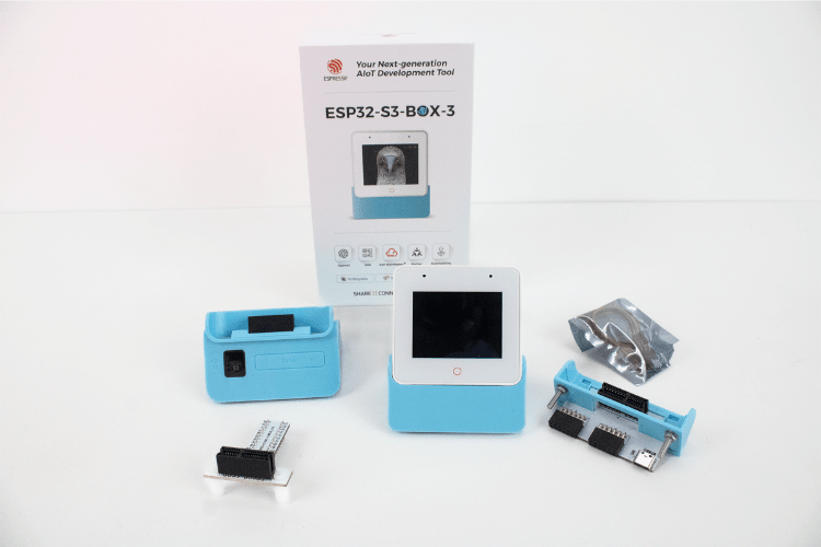
Finding the right ESP32-S3 development kit often means compromising between functionality and deployment readiness. With so many ESP32-S3 dev kits out there, we have been searching for a ready-to-deploy module that doesn’t require extra work like designing enclosures or 3D printing cases. These things can significantly increase the deployment time. One such kit we found is Espressif’s ESP32-S3-BOX-3.
CircuitDigest presents the Smart Home & Wearables Project Contest 2025! Win exciting prizes worth up to ₹7,00,000 and receive free development boards through our partnership with DigiKey. For registration, dive into contest details.
This isn't just another development board thrown into a generic case. The ESP32-S3-BOX-3 development board is a modern kit designed for AIoT, Edge AI, and industrial IoT projects. The ESP32-S3-BOX-3 runs on the ESP32-S3 chip technology, and it is housed in an attractive, pre-assembled case to ensure you can get started without any extra work. You also have plenty of options to expand to easily customise for different project scenarios. It is compatible with Espressif’s software platform choices, such as ESP-BOX, ESP-SR, ESP-Rainmaker, and ESP-Matter, enabling everything from quick prototypes up to full-featured IoT applications. With such a clean design and flexible features, this modern kit is certainly a worthy addition to the development board category.
With all these features, it makes a perfect choice for our upcoming Smart Home and Wearable Project Challenge, where you can win prizes of up to Rs. 7,00,000. You can also win a development board and some cool goodies just by sharing your project ideas. So don’t forget to check out the Smart Home and Wearable Project Challenge for more details.
Let’s take a closer look at the ESP32-S3-BOX-3.
What's Included in the ESP32-S3-BOX-3 Development Board Package?
The unboxing is a little interesting as we get a lot of usable accessories with the ESP32-S3-BOX-3 kit. Below you can see the unboxing image.
This dev kit comes with the following accessories,
ESP32-S3-BOX-3:
The main unit that can work on its own
ESP32-S3-BOX-3-DOCK:
A functional accessory serving as a stand for the main box
ESP32-S3-BOX-3-SENSOR:
A functional accessory showcasing sensor applications
ESP32-S3-BOX-3-BRACKET:
An adapter accessory for mounting the main box to other devices
ESP32-S3-BOX-3-BREAD:
An adapter accessory for easy connection of the main box to a standard breadboard
A USB-C:
Power cable
RGB LED Module and Dupont Wires:
For testing
We received all this in a little big box. Inside were foam moulds holding all the accessories in place. It’s nicely packed. It might be tricky to perfectly place all the components back in the same spot again. Sometimes it gets confusing to repeat, as all the accessories are tightly packed. So, remember the positions of components while taking them out.
Next, let’s look at the feature that makes us more excited about this dev kit.
Key Features of the Espressif ESP32-S3-BOX-3
To make this development kit outstanding and usable for AI and IoT applications, it comes packed with a rich set of features.
ESP32-S3-BOX-3 Quick Reference
ESP32-S3 Dual-Core Microcontroller –
Powerful dual-core Xtensa 32bit LX7 processor running up to 240 MHz with built-in Wi-Fi and Bluetooth connectivity.
Generous Memory Configuration –
512 KB SRAM and 384 KB ROM for robust application development, plus 16 MB Octal SPI PSRAM and 16 MB Quad SPI External Flash for extensive storage.
Advanced AI Capabilities –
Built-in neural network processing, acoustic algorithms, and computing acceleration for vector operations, complex numbers, and FFT calculations.
2.4-inch Colour LCD Display –
Crisp 240 x 320 pixel resolution display with SPI interface running at 40 MHz, driven by ILI9342C controller for vibrant visuals.
10-Point Capacitive Touch Screen –
Multi-touch support for intuitive user interaction and gesture recognition.
Wireless Connectivity –
2.4 GHz IEEE 802.11b/g/n Wi-Fi with Bluetooth 5 LE and Bluetooth mesh support for versatile IoT applications.
High-Quality Audio System –
Dual microphone setup with EST2210 ADC model, mute support, 8 Ohm 1W speaker with NS4150 PA model, and ES8311 codec for crystal-clear audio processing.
Advanced Motion Sensing –
3-axis gyroscope and 3-axis accelerometer (ICM-42607-P sensor model) for motion detection and orientation tracking.
Versatile Interface Options –
USB Type-C port for power, USB download/JTAG debug, and general USB device functions, plus Goldfinger connector for I/O expansion.
User-Friendly Controls –
Onboard Reset, Boot, and Mute buttons with Power LED and Mute LED indicators for easy operation and status monitoring.
Experimental High-Speed PSRAM –
120 MHz PSRAM speed capability for demanding real-time applications.
Compact and Lightweight Design –
Measuring just 61 x 66 x 16.6 mm and weighing only 292g, perfect for portable projects.
Flexible Power Options –
USB-C power input (5V - 2.0A) with no battery dependency for continuous operation.
Professional Development Support –
Ships with FreeRTOS and supports ESP-IDF SDK for professional embedded development.
On the software side, it can be programmed with ESP-IDF or Arduino IDE, and it supports various AI frameworks for machine learning applications. The combination of powerful processing capabilities and rich sensor integration makes it ideal for voice recognition, image processing, and intelligent IoT projects.
ESP32-S3-BOX-3 Applications and Use Cases
Let me add some of the possible applications of this ESP32-S3-Box-3 development board, which will give you a better idea.
Smart Home Control: Voice commands, touch interface for lights, appliances, and security systems
Voice Assistants: Custom wake word detection, speech recognition, and audio response systems
Industrial HMI: Machine control panels, process monitoring, and operator interfaces
AI Edge Computing: Real-time object detection, facial recognition, and predictive analytics
Interactive Displays: Digital signage, information kiosks, and customer engagement systems
Healthcare Monitoring: Patient vitals tracking, medication reminders, and wellness applications
Educational Projects: IoT learning platforms, STEM demonstrations, and programming tutorials
Motion Control: Gesture recognition, orientation sensing, and movement-based interfaces
Audio Processing: Sound analysis, noise monitoring, and acoustic pattern recognition
Wireless IoT: Remote monitoring, data collection, and cloud-connected applications
Prototyping Platform: Rapid development of AI-powered devices and smart solutions
Environmental Sensing: Climate monitoring, air quality tracking, and automated responses
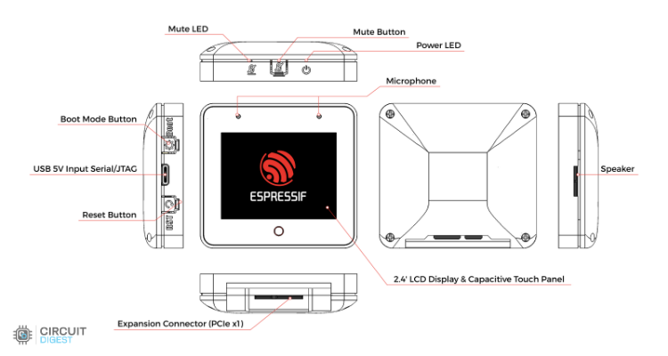
ESP32-S3-BOX-3 Development Board: Physical Overview
Now that we know all the features, let’s move to the physical overview. Since the Espressif Systems esp32 s3 box 3 aiot kit comes with multiple accessories, we'll look at each part, starting with the main unit.
ESP32-S3-BOX-3 Main Unit
The main highlight of the ESP32-S3-BOX-3 is its compact form factor with a boxy design.
Above, you can see all the peripherals marked in the orthographic view.
It has some unique built-in peripherals like a small 2.4” LCD with capacitive touch support, a pair of microphones at the top of the front screen, a customizable touch button (marked as O) below the display, a speaker on the right, a boot mode selection button, a reset button, and a USB Type-C port on the left side. On the top, you’ll find a mute button, power and mute LED indicators, and finally, a beautiful PCIe X1 connector where all the accessories can be attached.
And now, let’s look in detail at each component and some of the internals.
Microcontroller
Chipset: ESP32-S3
CPU: Dual-Core Xtensa® 32-bit LX7, up to 240 MHz
SRAM: 512 KB
ROM: 384 KB
PSRAM: 16 MB (Octal SPI, 120 MHz experimental)
External Flash: 16 MB (Quad SPI)
Memory & AI Features
AI Support: Neural Network, Acoustic algorithm support
USB Type-C: Power, USB download, JTAG debug, general USB device functions
Goldfinger (PCIe x1 style): Provides GPIO & power I/O expansion
OS / SDK
OS: FreeRTOS
SDK: ESP-IDF
Power
USB-C Input: 5 V, 2.0 A
Battery: Not available
Outline
Dimensions: 61 × 66 × 16.6 mm
Weight: 292 g
That’s all packed inside the ESP32-S3-BOX-3 itself. Now, let’s move on to the kit accessories.
ESP32-S3-BOX-3 Accessories Comparison
Accessory
Primary Function
Best Use Case
DOCK
Stand with Pmod headers, USB-A port
Desktop projects, USB peripherals
SENSOR
Temp/Humidity, Radar, IR, Battery
Environmental monitoring, portable apps
BRACKET
Mounting adapter
Retrofitting existing devices
BREAD
Breadboard adapter
Prototyping and testing
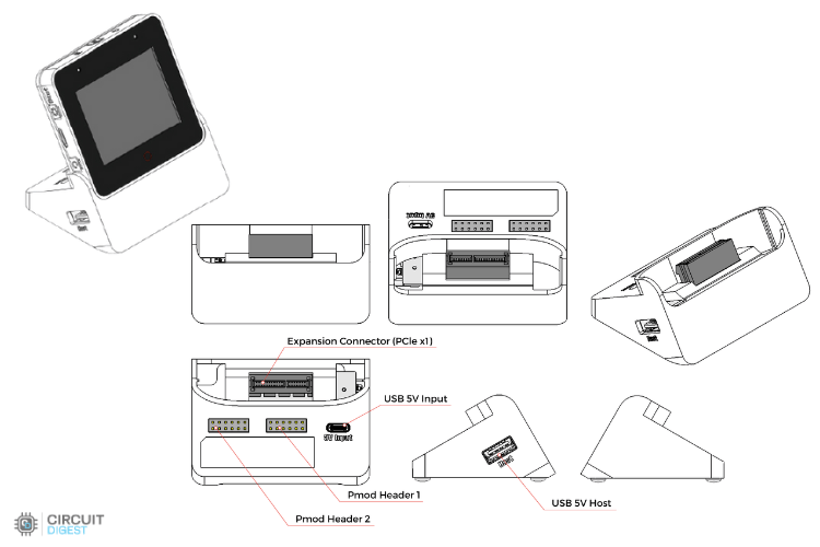
ESP32-S3-BOX-3-DOCK Expansion Module
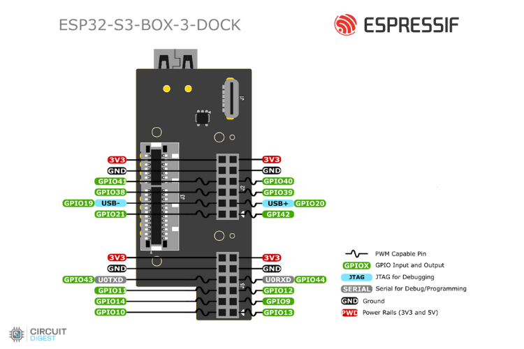
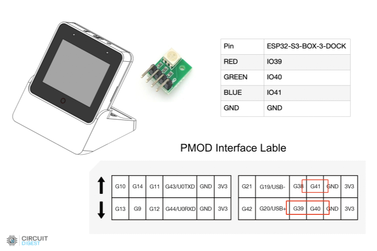
ESP32-S3-BOX-3-DOCK is designed to serve as a stand for the ESP32-S3-BOX-3 via its gold fingers and offers versatile expandability. It features two Pmod™ compatible headers, allowing users to connect additional peripheral modules. These headers provide 16 programmable GPIOs and can supply 3.3 V power to peripherals. There is one USB Type-A port for connecting devices such as USB cameras (up to 720p resolution), USB drives, and other HID devices. Another USB Type-C port is dedicated to 5 V input power only.
Here’s the orthographic view of the dock. It looks simple, but it actually has four different connectors. Let’s dive into their technical details.
Connectivity Interfaces
12-pin Female Headers (2x)
I/O Count: 8 I/O per header
Compatibility: Pmod™ Compatible
Power Output: 3.3V
Supported Protocols: GPIO, I2C, SPI, UART, RMT, LEDC, etc.
USB Type-A Port (1x)
Power Output: 5V
Functionality: USB Host capability
Compatible Devices: USB cameras, USB storage devices, HID devices
Next is the pinout diagram of the dock. There’s also a label on the dock itself for quick reference.
Next, let’s look at the ESP32-S3-BOX-3-SENSOR.
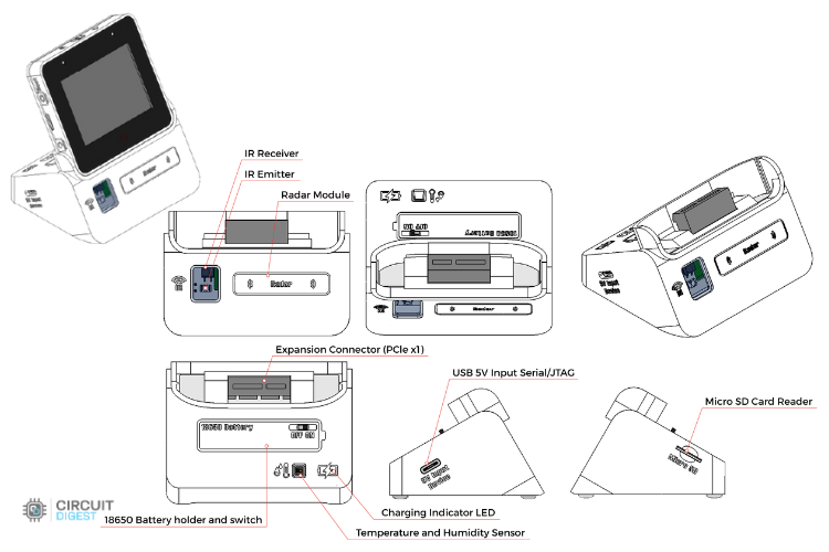
ESP32-S3-BOX-3-SENSOR
ESP32-S3-BOX-3-SENSOR is a versatile accessory integrating a Temp & Humidity sensor, IR emitter and receiver, radar sensor, 18650 rechargeable battery slot, and MicroSD card slot. It enables users to create a wide range of innovative projects easily. You can integrate multiple sensors for detection and control, use the rechargeable battery for portability, and expand storage with a MicroSD card (up to 32 GB).
Below you can see the Orthographic View of the ESP32-S3-BOX-3-SENSOR.
Sensing Capabilities
Radar Sensor - MS58-3909S68U4 (1x)
Operating Frequency: 5.8 GHz
Power Consumption: 40 μA (ultra-low power)
Detection Range: Approximately 2 meters
Application: Human presence detection
Technology: Microwave radar sensing
RI_SDA - IO41, RI_SCL -IO40, RI_OUT - IO21
Infrared Sensor Array (2x)
Emitter: IRM-H638T IR emitter tube [GPIO39]
Receiver: IR67-21C/TR8 receiver tube [GPIO38]
Range: Up to 4 meters effective distance
Application: Infrared control and remote sensing
Configuration: Paired emitter-receiver setup
Temperature & Humidity Sensor - AHT30 (1x)
Temperature Range: -40°C to +120°C
Temperature Accuracy: ±0.5°C
Humidity Range: 0% to 100% RH
Humidity Accuracy: ±3% RH (at 25°C)
Application: Environmental monitoring and climate control
AHT21_SCL - IO40, AHT21_SDA - IO41
Storage & Power Management
External Storage (1x)
Type: MicroSD card slot
Maximum Capacity: 32GB
Usage: Data logging, firmware storage, media files
Function: Battery charging and discharging protection
Safety: Prevents 18650 battery damage from over-discharge
Status & Interface
Charging Indicator LED (1x)
Red State: Battery charging in progress
Green State: Battery fully charged
Usage: Visual battery status monitoring
USB Type-C Port (1x)
Power Input: 5V
Functions: Power supply, USB data transfer, JTAG debugging
Compatibility: Standard USB device functions
PCIe Connector (1x)
Type: 36-pin, 1.00mm (0.0394") pitch
Card Compatibility: 0.062" (1.60mm) thickness
Mounting: Vertical goldfinger connector
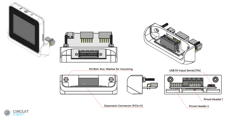
ESP32-S3-BOX-3-BRACKET
ESP32-S3-BOX-3-BRACKET helps mount the ESP32-S3-BOX-3 to other devices, unlocking many possibilities for turning non-smart devices into smart ones. Installation is straightforward; just prepare two mounting holes and a slot using the provided template. By leveraging its two Pmod™ compatible headers, you can add wireless connectivity, voice control, and screen control features. The bracket allows you to maximise the potential of your non-smart devices.
Below is the orthogonal view of ESP32-S3-BOX-3-BRACKET,
Connectivity
12-pin Female Headers (2x)
I/O Count: 8 I/O per header
Compatibility: Pmod™ Compatible
Power Output: 3.3V
Protocols: GPIO, I2C, SPI, UART, RMT, LEDC, etc.
USB Type-C Port (1x)
Input Voltage: 5V
Functions: Power supply, USB download, JTAG debug
Usage: Development and general USB device functions
PCIe Connector (1x)
Specifications: 36-pin, 1.00mm (0.0394") pitch
Card Support: 0.062" (1.60mm) thickness cards
Type: Vertical mounting goldfinger
Mounting Hardware
M3 Mounting Bolts (2x)
Bolt Size: M3 threading
Includes: Bolt, nut, and washer per set
Purpose: Secure mounting and component assembly
Usage: Attach materials and fasten components together
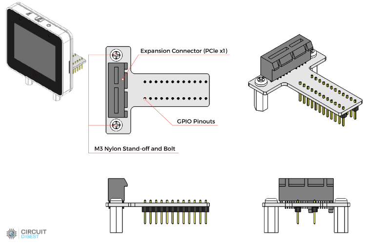
ESP32-S3-BOX-3-BREAD
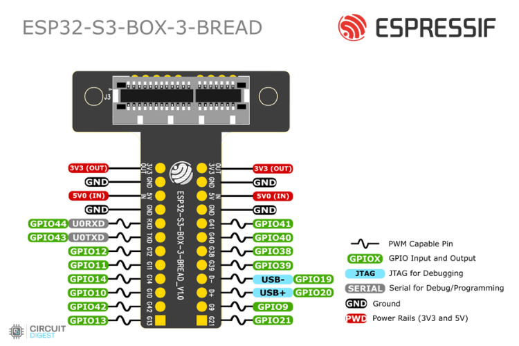
ESP32-S3-BOX-3-BREAD is an adapter that lets you easily connect the ESP32-S3-BOX-3 to a standard breadboard. It’s ideal for makers and DIY projects, using a high-density PCIe connector and two rows of 2.54 mm pitch pins to expose the ESP32-S3’s 16 programmable GPIOs.
Interface Headers
12-pin Male Headers (2x)
I/O Configuration: 8 I/O pins per header
Power Specifications: 3.3V output, 5V input capability
Protocol Support: GPIO, I2C, SPI, UART, RMT, LEDC, etc.
Design: Male connector for breadboard compatibility
Development Interface
USB Type-C Port (1x)
Input Power: 5V
Functionality: Power input, USB download, JTAG debugging
Usage: Development programming and general USB device operations
Expansion
PCIe Connector (1x)
Format: 36-pin, 1.00mm (0.0394") pitch
Card Thickness: Accepts 0.062" (1.60mm) cards
Mount Type: Vertical goldfinger connector
Application: Hardware expansion and prototyping
Key Differences from Other Variants
Male Headers: Unlike other variants with female headers, this uses male pins for direct breadboard insertion
Dual Voltage: Headers support both 3.3V output and 5V input
Prototyping Focus: Designed specifically for breadboard-based development and experimentation
With this, you should now have a solid understanding of the ESP32-S3-BOX-3 and its accessories, along with the pinouts and used IOs.
ESP32-S3 Development Board Schematic and Technical Documentation
Espressif has provided plenty of documents for the esp32-s3-box-3 development board. If you are new to development or programming and want to learn more, the documents are worth reviewing. There is a "docs" section in their GitHub repo that contains a “docs” section with everything from a hardware overview to PCB and schematic files.
Keep in mind, the native support is for ESP-IDF.
Through Espressif's official repo, you can access the complete schematic for the ESP32-S3 development board, PCB design files, a bill of materials (BOM), and details about hardware documents. Still, if you know the pins and have some basic knowledge, you can use the Arduino IDE to program the ESP32 S3 Box 3.
The ESP32-S3-BOX-3 comes with ready-to-use firmware that supports offline voice wake-up and speech recognition in both Chinese and English. With the ESP-BOX mobile app, you can set up AI voice interactions and create custom commands to control your smart devices. The firmware also includes several sensor demos and supports IR learning, so the box can even act as a controller for your home air conditioners. This ESP32-S3-BOX-3 tutorial will guide you through every step.
Initial Setup and Power-On
⇒ Step 1: Powering the Device
Power on your device using the USB-C cable. Once powered, within a few seconds, you will see the Boot Screen Animation.
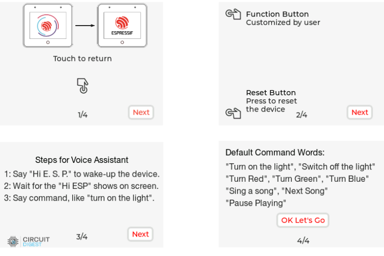
⇒ Step 2: Learning the Basics
After the first successful boot, you will see a quick guide provided by the device, like the four screens shown below.
The first two pages of the quick guide give an overview of the buttons on your ESP32 S3 box 3. Press the Next button to proceed to the next page. The following pages explain how to use AI voice control. Tap OK, Let’s Go to access the menu.
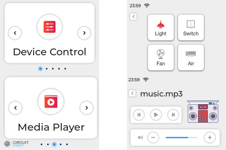
⇒ Step 3: Main Menu Exploration
The menu has six options: Sensor Monitor, Device Control, Network, Media Player, Help, and About Us. You can navigate between these options by swiping left or right.
For example, to access the Device Control screen, tap on Light to toggle the light on or off. After that, return to the menu, go to the Media Player screen, and either play music or adjust the system volume.
Testing Factory Firmware
⇒ Step 4: Quick Testing
Device control and voice commands are a quick way to test the Espressif ESP32-S3-Box-3. To continue, you need to connect the provided RGB Light to the dock’s header pins.
Connections are shown in the image below:
Now, in the UI, go to Device Control. By pressing the Light button, you can turn the light on or off.
You can also use voice commands like,
"Turn on the light" "Switch off the light" "Turn Red" "Turn Green" "Turn Blue" The LED will respond. Don’t forget to say the wake word before giving commands.
Connecting to ESP-BOX Mobile App
⇒ Step 5: Advanced Feature Testing
So far, all features have been tested offline. Now, let’s move online with a few simple steps.
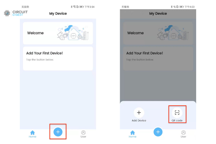
First, download the ESP-BOX app to your phone. It’s simple: go to Network, and in the top-right corner, click the button to install the app. You will see a QR code to download it.
After installing the app, sign in with your ESP-BOX account. Turn on Bluetooth on your phone, tap + at the bottom of the screen, and scan the QR code on your device to set up the network.
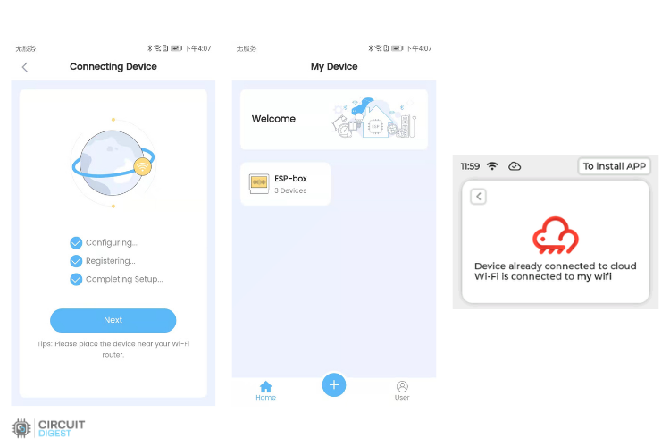
After adding the device, you will see prompts like these in the image below.
Remember:
Do not exit the QR code page during network setup.
Connect the device to 2.4 GHz Wi-Fi, not 5 GHz, and enter the correct password.
An incorrect password will trigger "Wi-Fi Authentication Failed."
Long-press the Boot button (Function button) for 5 seconds to clear network information and restore factory settings. If the QR code or Bluetooth does not work after resetting, restart your device using the Reset button.
After successfully adding the device, select it in the app. You can control the device here as well. Unlike the first time, it uses ESP RainMaker for communication.
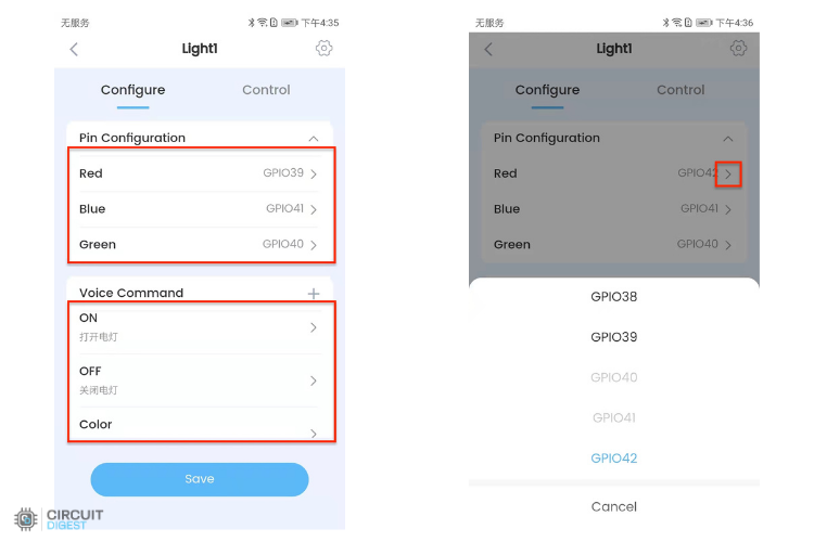
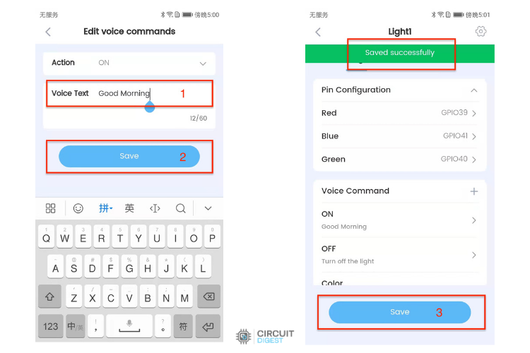
Tap on the icon to access the Config Menu. Here, you can configure pins directly.
In Voice Command, you can add custom commands. Enter the text and its action, for example, set "Good Morning" to turn on the light. Click Save to return to the previous screen, then click Save again.
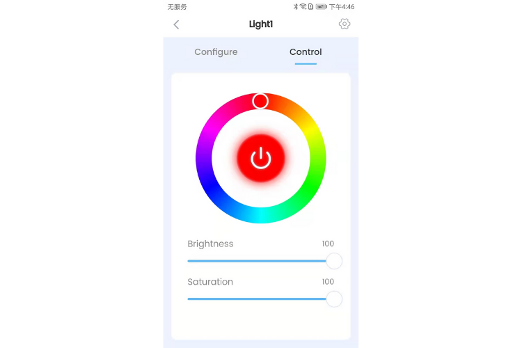
In the Control tab, you can directly configure the LED from the app, adjusting colour, brightness, and saturation.
Working with Sensor Accessories
⇒ Step 6: Testing the Given Accessory
Among the accessories provided, the sensor module is the most unique, as it includes multiple sensors to work with, while the others mainly extend connectors for breadboard use. Additionally, it supports different orientations and mounting options.
The ESP32-S3-BOX-3-SENSOR is a versatile accessory that integrates a Temperature & Humidity sensor, a pair of IR Emitters and Receivers, and a Radar sensor. It allows users to easily create sensor networks and other sensor-based applications. The built-in firmware provides a real-time display of temperature and humidity, demonstrates human presence monitoring through a 2.4 GHz radar, and includes an IR learning interface. This lets you use the ESP32-S3-BOX for IR learning of your air conditioner, enabling remote control. The learning feature also works with other in-home IR controllers, such as fans, TVs, and projectors, making the experience interactive and engaging.
Temperature and Humidity Sensor
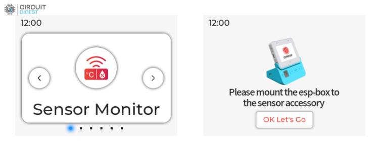
Go to the Sensor Monitor. The interface will prompt you to insert the sensor accessory.
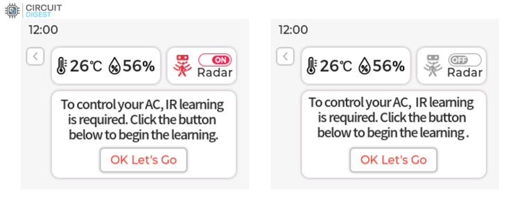
After mounting the accessory, you will be able to see the temperature and humidity readings on the screen.
Radar Feature
To use the radar, enter the Sensor Monitor screen and tap the ON/OFF button to enable or disable radar monitoring. When the radar switch is ON, a red body icon will appear if a person is detected in front of the device. The icon will turn gray if no one is detected within two minutes.
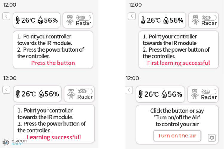
IR Learning
Below the temperature, humidity, and radar functions is the infrared learning module. Currently, this module can only learn the ON/OFF function of a remote controller. Follow the interface instructions to iteratively learn the ON/OFF command of your remote a total of four times. After successful learning, the interface will confirm it.
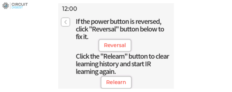
Perform an ON/OFF test on your air conditioner by pointing the ESP32-S3-BOX-3-SENSOR toward it. If the air conditioner’s ON/OFF behaviour is opposite to what you expect, click the Reversal button to correct it. You can also click Relearn to learn commands from other remote controllers.
Remember
When the ESP32-S3-BOX-3 is not mounted to the ESP32-S3-BOX-3-SENSOR dock, the entire Sensor Monitor function will not work.
While using the built-in firmware with the ESP32-S3-BOX-3-DOCK, avoid hot-plugging the dock or switching to the Sensor Accessory, as this may cause the accessory to be unrecognised. Simply power the ESP32-S3-BOX-3-SENSOR again to restore normal operation.
Due to the power limitations of the infrared emitter and differences among air conditioner brands, the effective range for IR learning has been tested to be between 1 and 1.5 meters.
The features of the Box are not limited to the factory firmware; it’s mainly for demonstration purposes. To truly unleash the power of this device, you need to use ESP-IDF. I wouldn’t recommend the Arduino IDE, as many components supported in ESP-IDF don’t have full support in the Arduino IDE. To access all features, it’s best to stick with ESP-IDF.
There are up to 10 example programs available in Espressif’s official ESP-BOX Git repository,
chatgpt_demo
esp_joystick
factory_demo
image_display
lv_demos
matter_switch
mp3_demo
usb_camera_lcd_display
usb_headset
watering_demo
These samples illustrate different aspects of what the board is capable of, and provide useful ideas to get you started with your own projects. This development board offers plenty of functionality within a compact, ready-to-use board. Regardless, if you are prototyping or building larger applications, it's worth analysing what each application provides. For now, take some time to work through the examples to see how they relate to your own project ideas.
So, enjoy exploring this dev board! With it, you can do a lot and really learn while having fun.
For wearable projects, having the right sensor module makes all the difference. As you all know, this year’s contest theme is Smart Home and Wearables, so we came up with another sensor module, the MAXREFDES117 optical heart-rate module. This device comes with integrated red and IR LEDs, making it an ideal choice for developers and enthusiasts alike. The MAXREFDES117 optical heart rate module is a compact, low-power sensor designed specifically for wearable health monitoring projects.
Purchasing electronic components from international suppliers can often be a complicated process for customers in India. Traditional ordering from DigiKey in USD requires managing customs clearance, local freight, and cross-border payments, which can be time-consuming and prone to errors. To facilitate electronic component sourcing in India, DigiKey has aligned itself with AqTronics India, an electronics distributor certified in local logistics, to offer easy and seamless payment options for Indian buyers through DigiKey India. Whether you are an electronic hobbyist, a startup, or an established organisation, knowing how to buy at DigiKey using AqTronics will simplify your electronic component sourcing process. This partnership allows buyers to pay in Indian Rupees, receive GST-compliant invoices, and enjoy hassle-free door-to-door delivery.
CircuitDigest presents the Smart Home & Wearables Project Contest 2025! Win exciting prizes worth up to ₹7,00,000 and receive free development boards through our partnership with DigiKey. For registration, dive into contest details.
One of the key advantages of using AqTronics as the logistics partner is the simplification of the import process. Customers no longer need to obtain an Import Export Code (IEC) or handle customs clearing procedures themselves. AqTronics takes care of local freight and customs clearance, ensuring that orders reach the customer quickly and efficiently. For most locations in India, deliveries are completed within one to two working days after dispatch from AqTronics’ warehouse in Bangalore, making the entire process far more convenient than navigating international shipping independently.
Author Expertise: This comprehensive DigiKey India purchase guide is based on Circuit Digest's hands-on experience with successfully placing multiple orders through AqTronics as the authorised local logistics partner.
Key Benefits of Using AqTronics as DigiKey's Local Logistics Partner
The partnership between DigiKey and AqTronics India electronics distributor, offers several advantages for how to buy electronic components from DigiKey in India:
1. Simplified Import Process for Electronic Components Sourcing India 2. Financial Convenience with Local Payment Options 3. Reliable Access to Global Electronics Distributor Inventory
Another significant benefit is the financial ease it provides. Payments are made in INR through familiar Indian payment gateways, reducing foreign exchange risks and eliminating the complexities of cross-border transactions. Customers also receive official invoices from AqTronics Technologies, which are fully compliant with Indian GST regulations. This makes accounting simpler for businesses and hobbyists alike, aligning with local financial processes. Apart from that, using AqTronics ensures reliable support and access to the same wide product range offered by DigiKey. While the ordering process is handled locally, the products themselves are sourced directly from DigiKey, maintaining product quality and consistency. In addition, any issues or inquiries can be addressed through local customer service representatives, providing peace of mind and a smoother overall purchasing experience. By combining local expertise with DigiKey’s global inventory, AqTronics makes it easier than ever for Indian customers to access the components they need.
Complete DigiKey India Purchase Guide: Step-by-Step Process
⇒ Step 1: DigiKey India Account Setup and Registration
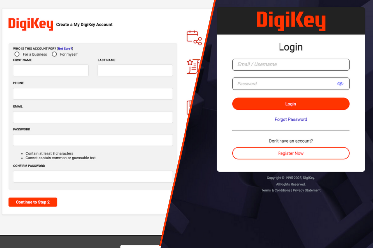
Before you begin, note that only registered DigiKey users can purchase using the local logistics partner. If you are a new user, create an account on DigiKey; it’s free and takes only a few minutes. Existing users can simply log in with their credentials.
Note: If you are registering as a new user, you will have to wait for the verification email from DigiKey. This usually takes 3-4 hours or more, depending on your region and time of registration.
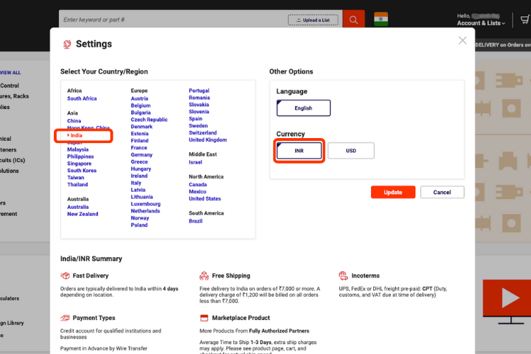
After logging in, locate the country flag icon next to the search bar on the header menu. Make sure India is selected as your country. If you need to change it, click on the flag icon to open a settings window, then select India as the country and INR (Indian Rupee) as the currency.
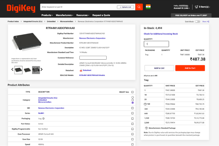
⇒ Step 2: Adding Electronic Components to Your Cart
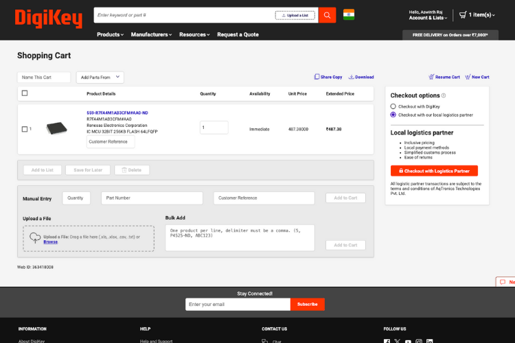
Next, add the items you wish to purchase to your shopping cart.
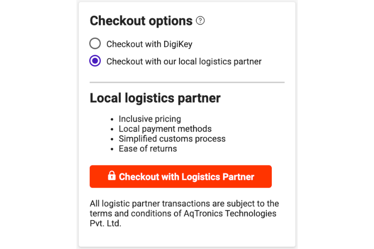
Once all items are added, click the shopping cart icon at the top left to view your selections. On this page, you will see two checkout options: Checkout with DigiKey and Checkout with our local logistics partner. Note that the prices displayed are in INR and do not yet include customs taxes, which will be calculated later.
⇒ Step 3: Checkout Process with AqTronics India Electronics Distributor
Under the checkout options, select Checkout with our local logistics partner. Clicking this option will change the checkout button to Checkout with our local logistics partner, and clicking on it will automatically transfer your order details to the AqTronics website for further processing.
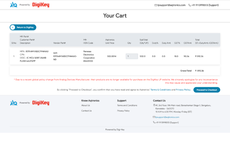
On the AqTronics checkout page, you will see the duty amount and GST fees applied to each item. The total at the bottom includes customs duties, GST, and shipping charges in INR. Once reviewed, click the “Proceed to Checkout” button to continue.
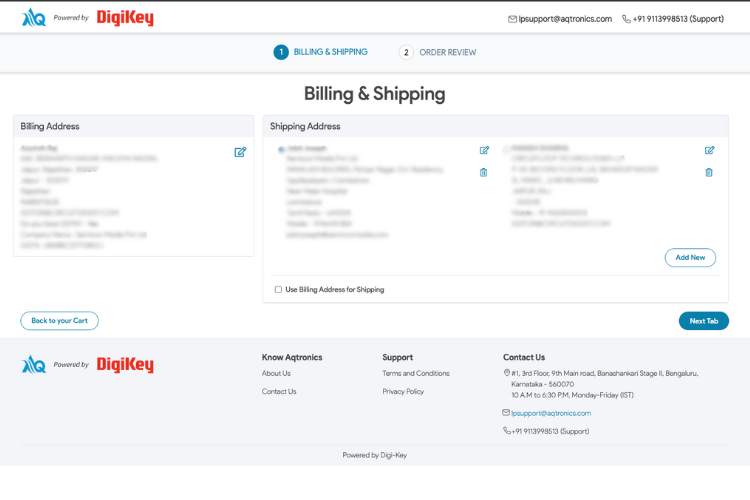
Provide your billing and shipping address carefully to ensure smooth delivery. For business orders, enter your GST number along with the billing address. Once all details are filled, click on “Next Tab” to continue.
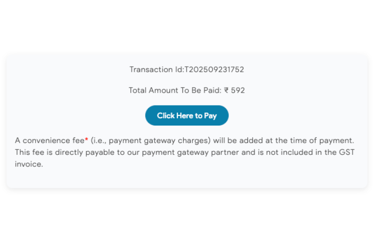
⇒ Step 4: Completing Payment Through the Indian Payment Gateway
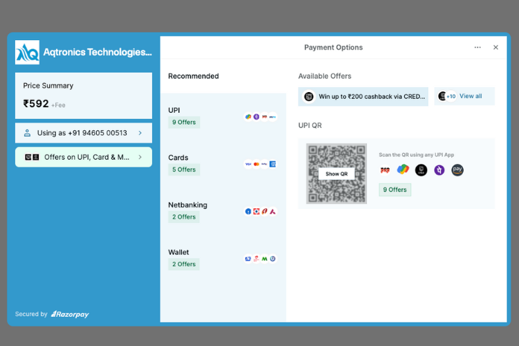
Review the total amount to be paid and click on “Click here to Pay.”
You will then be redirected to the Razorpay payment gateway, where you can complete your payment using UPI, debit or credit cards, net banking, or other supported online payment methods.
UPI payments (Google Pay, PhonePe, Paytm, BHIM)
Debit and credit cards (Visa, Mastercard, RuPay, American Express)
Net banking (all major Indian banks)
Digital wallets (supported e-wallets)
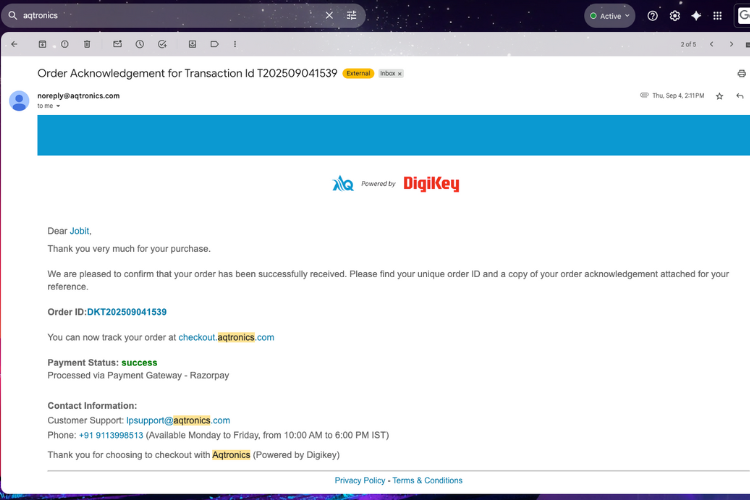
After completing the payment, your order will be successfully placed on DigiKey with AqTronics as your delivery partner. An order confirmation email, containing your order ID and tracking link, will be sent to your registered email address. Keep this email for reference.
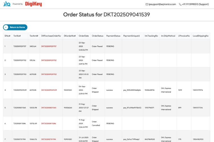
⇒ Step 5: Tracking Your DigiKey Shipping Process India
To track your order, visit the AqTronics website and enter your Order ID that you received via email in the above step. You will also receive all future status updates via email. Typically, deliveries within India take 7–10 business days.
⇒ Step 6: Delivery and GST-Compliant Invoice Receipt
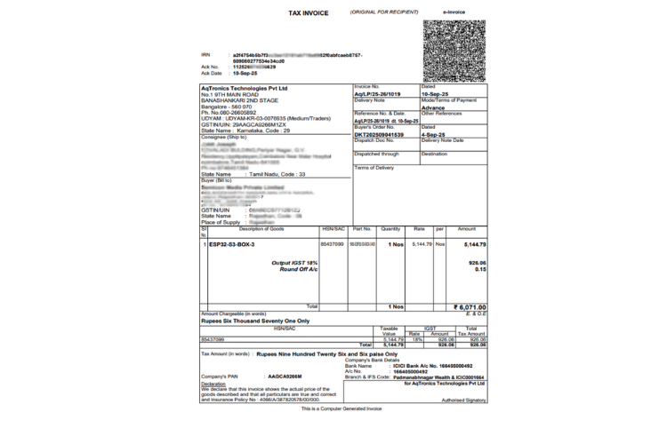
Orders placed through DigiKey using AqTronics are shipped first to the AqTronics fulfilment center and then delivered to your address using their local logistics network. AqTronics handles customs clearance and local delivery. GST-compliant invoices are shared via email once the order is shipped from the AqTronics warehouse, and a printed copy is provided with the delivery, ensuring full compliance with Indian tax regulations.
Frequently Asked Questions (FAQs) - DigiKey India Purchase
⇥ 1. Is an Import Export Code (IEC) required for ordering from DigiKey India through AqTronics?
The answer is no, AqTronics, which is the local logistics partner of DigiKey, takes care of all the import documentation and customs clearance for you, so it is very easy for both individuals and organisations to source electronic components without IEC registration.
⇥ 2. What payment methods are available for customers buying from DigiKey India through AqTronics?
DigiKey India payments through AqTronics are accepted in UPI (Google Pay, PhonePe, Paytm), debit/credit cards (Visa, Mastercard, RuPay, Amex), net banking from any major Indian bank, or selected digital wallets. All the payments will be done in INR via Razorpay's safe transaction gateway.
⇥ 3. Will I get a GST-compliant invoice for my DigiKey order?
Yes, AqTronics India electronics distributor, offers a complete GST-compliant invoice for every order. They have proper tax details, HSN codes, and are eligible for input tax credit. You are provided with both electronic copies through mail and a printed copy along with your shipment.
⇥ 4. Are the components sourced from DigiKey India legitimate and guaranteed?
Certainly! All electronic components are sourced from DigiKey's authorised global inventory, assuring 100% authenticity. These electronic components are guaranteed by the manufacturers, and you will receive the same components from DigiKey International as you would from DigiKey India, so you are assured of the same quality manufacturing by this global electronic components supplier..
⇥ 5. Can I cancel an order or make changes to an order once I've placed it with AqTronics?
Changes or cancellations should be made as soon as possible after your order is placed; you should contact AqTronics customer service 2-4 hours after your order is placed. If your order has been processed and shipped from DigiKey's international warehouse, the order cannot be cancelled. Changes must be communicated early.
⇥ 6. What are the steps to track my Digi-Key order through the AqTronics shipping method?
Simply go to the AqTronics URL and enter your Order ID (received in email) in the tracking section. You will receive an email notification as each shipping milestone goes through (customs clearance, out for delivery, etc.). The real-time tracking creates complete transparency for the DigiKey shipping process in India.
Related Resources: For technical specifications and component datasheets, visit DigiKey.in directly. For logistics inquiries, contact AqTronics customer support.
There have been many development boards recently built around the ESP32-S3. Most development boards come with a display, some also include cameras and buttons, and a few have speakers and microphones. Finding one that brings all these components together without compromising on quality has been the real challenge for makers and developers. Keeping all this in mind, we found a dev board that brings everything together in one module, the Adafruit MEMENTO.