Reverse Polarity Protection Circuit Using P-Channel MOSFET
You’ve just finished assembling an electronic project and are ready to power it up, only to realize the battery might be connected backwards. In an instant, a simple mistake can destroy hours of work. Reverse polarity is one of the most common causes of circuit failure, from hobby projects to industrial systems. The good news is that a well-designed reverse polarity protection using MOSFET technique can guard every circuit you build, with near-zero efficiency penalty.
A common way to protect a circuit from incorrect power connections is to use a diode, but it wastes energy and generates heat even when connected correctly. This can be a problem for low-voltage devices like battery-powered gadgets. A smarter solution is reverse polarity protection using a MOSFET, which acts as a small electronic switch that only lets power flow the right way, wastes very little energy, and helps the battery last longer. If you want to learn more about MOSFETs, how they’re constructed, their types, and how they work, check out this article: “What is MOSFET: Its Construction, Types and Working.”
Want to learn more about Electronic Circuits and practical project designs? Visit our page for easy tutorials and real-world applications. Start building smarter and safer electronics today!. A smarter solution is reverse polarity protection using a P-channel MOSFET, which acts as an electronically-controlled switch that conducts only under correct polarity, introduces a voltage drop of less than 0.1 V, and helps the battery last longer.
Table of Contents
- Understanding Reverse Polarity and Why Protection Matters
- Components Required
- Traditional Diode-Based Reverse Polarity Protection
- └ Efficiency Calculation
- Reverse Polarity Protection Circuit Using MOSFET (P-Channel)
- └ Step-by-Step Circuit Assembly
- How it Works
- Comparison
- Working Demonstration
- Enhanced P-MOSFET Reverse Polarity Protection with Zener Gate Clamping
- └ How the Zener Diode Protects the Gate
- How to Choose the Right MOSFET
Understanding Reverse Polarity and Why Protection Matters
Reverse polarity occurs when the positive and negative terminals of a power supply are connected incorrectly to a circuit. This can happen due to:
- Incorrect battery installation
- Miswired connectors
- Accidental connection of the wrong polarity power adapters
- Human error during prototyping or field installation
Without protection, reverse polarity can cause immediate component failure, permanent damage to ICs, or even thermal runaway leading to fire hazards.
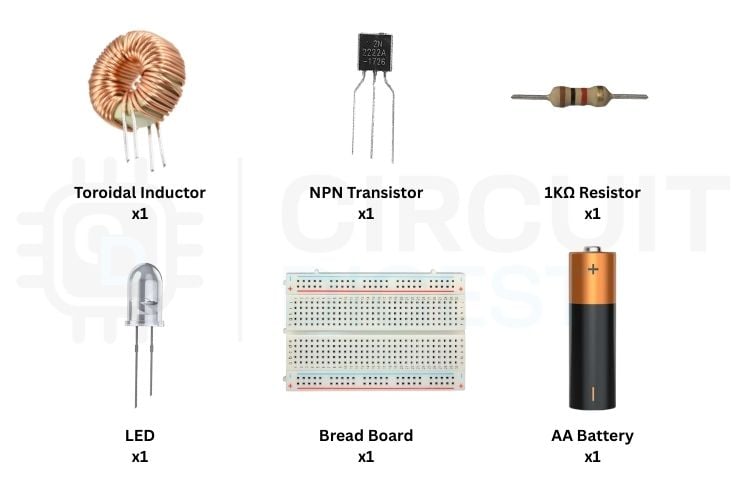
Components Required for Reverse Polarity Protection Circuit Using MOSFET
The following components are needed to build the MOSFET-based reverse polarity protection circuit.
| Components Name | Qty | Purpose |
| P-Channel MOSFET (IRF9710) | 1 | Main switching element for reverse polarity protection |
| Diode (IN4007) | 1 | Blocks current when power is connected in reverse. |
| Gate Resistor (1k ohms) | 1 | Limits gate current and stabilizes MOSFET switching |
| DC Power Supply / Battery | 1 | Provides input power to the circuit |
| Load (LED / Microcontroller / Motor) | 1 | Used to test circuit operation |
| Breadboard | 1 | Used for circuit assembly |
| Connecting Wires | As required | Used for making electrical connections |
Traditional Diode-Based Reverse Polarity Protection
The simplest method of reverse polarity protection uses a diode connected in series with the positive supply line. When the power supply is connected with the correct polarity, the diode becomes forward-biased and allows current to flow, with a typical forward voltage drop of around 0.7V. When the supply is connected in reverse polarity, the diode becomes reverse-biased and blocks the current flow, preventing current from reaching the circuit and protecting the connected components from damage.
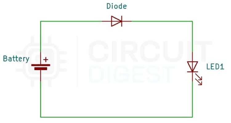
Although this method provides basic protection, it is not energy efficient. The forward voltage drop across the diode results in continuous power dissipation and reduced available voltage at the load.
Diode Method — Efficiency Calculation
For a 12V system operating at 500mA load current:
Power Loss = 0.7V × 0.5A = 0.35W
Efficiency Impact = (0.7 / 12) × 100% = 5.8% voltage loss
This power loss is converted into heat, which can affect thermal performance and battery life in portable systems.
Because diode-based protection wastes power and produces heat, a reverse polarity protection circuit using MOSFET is a better choice. It offers much lower voltage drop, higher efficiency, and improved overall power performance, making it ideal for battery-powered and high-current applications.
Reverse Polarity Protection Circuit Using MOSFET (P-Channel)
A P-channel MOSFET connected in series with the positive power line, with its gate connected to ground through a pull-down resistor, provides efficient reverse polarity protection with very low voltage loss. When the power supply is connected correctly, the gate to source voltage becomes negative, which turns the MOSFET ON and allows current to flow with very low resistance. When the supply polarity is reversed, the gate to source voltage becomes positive, keeping the MOSFET OFF and blocking the current flow. The internal body diode is oriented to prevent current flow during reverse connection, providing additional protection and ensuring reliable circuit operation.

Step-by-Step Circuit Assembly
- Place the IRF9710 P-Channel MOSFET on the breadboard and find, using the datasheet pin-out, where the Source (S), Gate (G) and Drain (D) are located.
- At the same time, connect a resistor of 1k ohm from the Gate to the Ground this is the pull-down that allows the Gate Voltage to be lower in value relative to Drain (assuming power is being applied to Drain).
- If you connect a 1N4007 diode in the Gate Bias path with the cathode connected to the Gate and the anode connected to Gnd, this will prevent there being reverse Gate Voltage when the power supply is reversed in polarity.
- Now connect the load (for example: LED + 470-ohm resistor, or an Arduino board using a similar circuit) between the Drain rail and GND.
- So when the power is applied with the correct polarity, the load (whether it be an LED or another load) will run as it should. If the power's polarity isn't correct, the load will not work.
MOSFET Method - Efficiency Calculation
To understand the efficiency advantage of MOSFET-based reverse polarity protection, consider the same 12V system operating at a load current of 500mA. Compared to diode-based protection, the MOSFET introduces significantly lower resistance in the current path, resulting in much smaller voltage drop and reduced power dissipation. This directly improves overall system efficiency and minimizes thermal losses, as shown in the following calculation.
Voltage drop = 0.5A × 0.1Ω = 0.05V
Power loss = 0.5A × 0.05V = 0.025W
Efficiency impact = (0.05/12) × 100% = 0.4% loss
Comparison: Diode vs MOSFET Reverse Polarity Protection
To clearly see the difference between diode protection and MOSFET protection, we can compare how both methods perform in real circuits. Even though both protect against wrong power connections, they differ in power loss, heat generation, and efficiency. The table below shows these main differences.
| Features | Diode Method | MOSFET Method |
| Voltage Drop | High (~0.6–0.8 V) | Very Low (~0.05–0.15 V) |
| Efficiency | Low | High |
| Heat Loss | High | Very Low |
| Cost | Cheap | Moderate |
| Current Handling | Limited | High |
| Reliability | Basic protection | More reliable protection |
Working Demonstration
In this video, both the diode-based protection circuit and the MOSFET-based protection circuit are tested to show their real-time behavior. When the power supply is connected correctly, both circuits allow current to flow and power the load. However, when the polarity is reversed, both circuits block the current and protect the connected components. The key difference can be observed in performance: the diode circuit shows a noticeable voltage drop and slight heating, while the MOSFET circuit delivers almost full supply voltage with very low power loss. This practical demonstration clearly shows why MOSFET-based reverse polarity protection is more efficient and reliable for modern electronic applications.
Enhanced P-MOSFET Reverse Polarity Protection with Zener Gate Clamping
The enhanced P-MOSFET reverse polarity protection circuit improves on the basic design by adding a Zener diode to protect the MOSFET gate from excessive voltage. In the simple MOSFET circuit, the gate voltage directly depends on the input supply. When higher input voltages or sudden spikes occur, the gate-to-source voltage can exceed safe limits and damage the MOSFET. The basic P-channel MOSFET reverse polarity protection circuit works well for supplies below ~20 V.
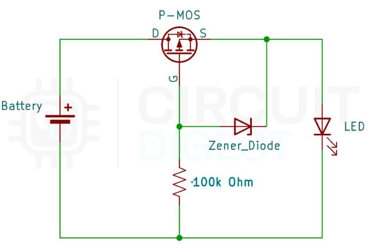
How the Zener Diode Protects the Gate
By adding a Zener diode, the gate voltage is clamped to a safe level, preventing overvoltage stress on the MOSFET. This makes the circuit more stable and reliable, especially in high-voltage or automotive and industrial applications. While the enhanced circuit uses one extra component, it provides better protection, improved durability, and safer long-term operation compared to the basic MOSFET-based reverse polarity protection circuit.
| Feature | Simple Circuit | Zener Protected Circuit |
| Reverse Polarity Protection | Yes | Yes |
| Gate Voltage Protection | No | Yes |
| Suitable for High Voltage | No | Yes |
| Component Count | Low | Slightly Higher |
| Reliability | Medium | High |
If you want to learn more about this enhanced circuit with the zener diode and see a detailed explanation, take a look at this article, “Reverse Polarity Protection Circuit”
How to Choose the Right MOSFET for Reverse Polarity Protection
Selecting the correct MOSFET for reverse polarity protection is critical for reliable and efficient operation. The following parameters should be checked from the datasheet before committing to a device:
| Parameter | What to Check | Recommended Value |
| VDS(max) | Must be greater than maximum supply voltage plus transient spikes | ≥ 1.5 × Vsupply |
| VGS(th) (threshold) | Must turn ON fully at your supply voltage; choose logic-level MOSFETs for 3.3 V/5 V | < Vsupply / 2 |
| RDS(on) | Lower is better — directly sets power loss and voltage drop | < 0.1 Ω for ≤5 A; < 0.01 Ω for ≥20 A |
| ID(max) | Must exceed peak load current with margin | ≥ 2 × maximum load current |
| VGS(max) | Determines whether a Zener gate clamp is needed | Typically ±20 V; add Zener if Vsupply > 15 V |
Real-World Applications of MOSFET Reverse Polarity Protection
The reverse polarity protection MOSFET circuit is a universal building block. The following applications benefit directly from the near-zero voltage loss it provides:
- Battery-powered devices
Protects gadgets when batteries are connected the wrong way. - Microcontroller projects
Keeps boards like ESP32 and Arduino safe during testing and development. - IoT and smart devices
Prevents damage in smart home sensors and automation systems. - Car electronics
Protects circuits in vehicles from accidental reverse battery connection. - Power supply inputs
Keeps adapters and power modules safe from wrong polarity connections. - Motor circuits
Protects motor drivers and controllers from wiring mistakes.
Conclusion
In conclusion, protecting circuits from wrong power connections is essential. While diode-based solutions work, they waste energy and generate heat. Reverse polarity protection circuit using a MOSFET provides a low-loss, efficient alternative that blocks reverse current, reduces heat, and extends battery life, making it ideal for both hobby and commercial projects. A well-designed reverse polarity protection circuit using a MOSFET resolves both issues: it conducts with a voltage drop of less than 0.1 V, generates negligible heat, handles high currents with the right device selection, and adds only two or three low-cost components to any design. Whether you are building a hobby project, a commercial IoT device, or an automotive accessory, P-channel MOSFET reverse polarity protection is the engineering best practice that every power input stage should include. Therefore, P-channel MOSFET reverse polarity protection should be considered a best practice in all power input stage designs, regardless of whether they are for a hobby project, commercial IoT device, or automotive accessory.
Frequently Asked Questions on Reverse Polarity Protection using MOSFET
⇥ 1. Can this circuit be used with batteries?
Yes, it is ideal for battery-powered devices because it reduces power loss and heat generation.
⇥ 2. Is MOSFET-based protection safe for high current circuits?
Yes, if the correct MOSFET is selected, it can safely handle high current loads.
⇥ 3. Can I use an N-channel MOSFET for reverse polarity protection?
Yes, you can use an N-channel MOSFET, but the circuit is more complex. It is usually placed on the ground side, and using it on the positive side requires extra control circuitry. For simple designs, a P-channel MOSFET is easier to use.
⇥ 4. Is it better to use a MOSFET instead of a diode for reverse polarity protection?
A MOSFET provides more efficient reverse polarity protection than a diode because its voltage drop is much lower (typically 0.05–0.15 V versus 0.6–0.8 V). This greatly reduces power dissipation and heat generation, especially in high-current applications.
Therefore, a MOSFET is preferable in battery-powered systems where efficiency and maximum available voltage are important.
⇥ 5. How can a P-Channel MOSFET be used to provide reverse polarity protection?
A P-channel MOSFET is placed in series with the positive supply rail for reverse polarity protection. With correct polarity, a negative VGS turns it on and allows current to flow. If polarity is reversed, VGS becomes positive, turning it off and blocking reverse current.
⇥ 6. Can this Protection Circuit Work with Arduino or ESP32 Boards?
Yes! Use a logic level P-MOSFET (e.g., AO3401, VGS(th) ≈ −1 V) on the 5 V or 3.3 V rail that powers the microcontroller board's VIN pin. The MOSFET will fully turn ON at these low voltages, provide only approximately 1-5mV of voltage drop, and completely protect the board from reverse power connection without any effect on the normal operation of the board.
⇥ 7. Why do some circuits include a Zener diode on the gate of a P-MOSFET?
MOSFET gates are typically limited to about ±20 V VGS, and voltage transients can exceed this rating. A Zener diode between gate and source clamps VGS to a safe value. This protects the MOSFET from overvoltage damage.
Related MOSFET Projects and Tutorials
Practical tutorials demonstrating how MOSFETs are used as efficient electronic switches for logic-level conversion, power control, and DC motor driving in embedded and general electronics circuits.

Simple MOSFET Switching Circuit – How to turn on / turn off N-Channel and P-channel MOSFETs
Discover how to use MOSFETs for switching circuits. Learn about N-channel and P-channel MOSFET behaviour, gate control, key parameters, and practical tips for reliable operation.

Simple H-Bridge Motor Driver Circuit using MOSFET
In this circuit tutorial, we will discuss one of the most commonly used and efficient ways to drive DC motors -the H Bridge circuit.

Arduino DC Motor Speed Control using MOSFET Transistor
Learn how to control the speed of a DC motor using Arduino and a MOSFET. This guide covers component selection, circuit setup, coding, and practical demonstrations for building an efficient motor controller.

Bi-Directional Logic Level Converter using MOSFET
Learn how to build a bi-directional logic level converter using MOSFETs to safely interface devices operating at different voltage levels, with step-by-step instructions and circuit explanation.