At the recent Electronica 2026 expo, I had the chance to spend some time at the Quectel booth speaking with Vijay Prakash (Product Manager, Quectel) and exploring their latest lineup of AI-focused single-board computers and smart compute modules. Most of us are already familiar with popular SBC platforms like Raspberry Pi and NVIDIA Jetson boards from NVIDIA.
When Shailesh Kachi, Founder of Adevair Technologies, set out to build Securio, he found the market fragmented. There were AQI monitors that showed how bad the air was but did nothing about it, purifiers without awareness of local air conditions, and filters that didn’t know when they were worn out. He wanted something different…something unique…one could say a breath of fresh air.
Agam Robotics is a startup based in Bangalore that builds drone components, including flight controllers, GNSS modules, optical flow sensors, rangefinders, power distribution boards, and power modules. The company's stated focus is on building products from the bottom up within India, with PCB fabrication, assembly, enclosures, plastics, and aluminium heat-sink components all done in India.
The MAX32672FTHR is a compact development platform built around the MAX32672 for embedded evaluation and prototyping. It provides the key hardware resources needed for development, including onboard debugging, power management, user interface peripherals, and Feather-compatible expansion headers.
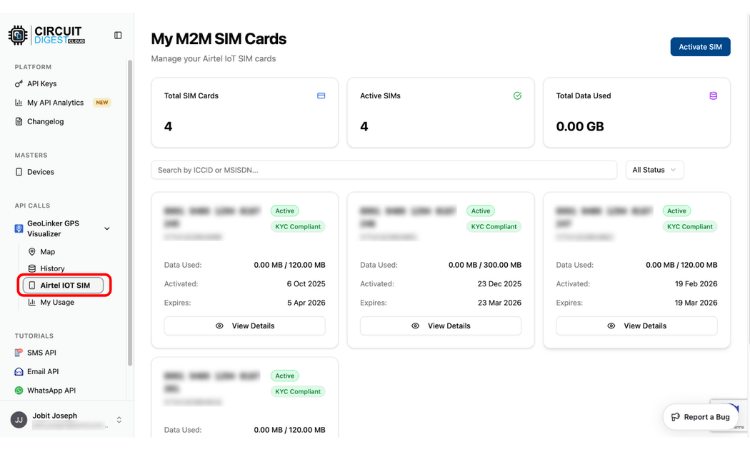
If you are working on IoT projects, you already know the importance of an M2M IoT SIM card for remote monitoring and tracking. For those who are new and wondering why you need a special M2M SIM card when you can just use your normal SIM card, here are two strong reasons to consider one.
Cost: If you are running a remote IoT device for a year and sending just a few MB of data every month, you will still have to spend at least 300 INR per month recharging your normal SIM cards (assuming Airtel and JIO have not increased their basic plans again). These standard user plans include voice, 2GB data per day, and subscriptions to OTT platforms, but all of this is wasted when using your SIM card with an IoT device. You will hardly consume a few MB of data every day, but still be forced to pay for a full package just to keep your SIM and device active. But with an M2M IoT SIM card, you can get data plans for as low as 30 INR per month if you are only using data.
Scaling: Now, say you are building a small pilot lot to test your own fleet of GPS trackers that you have just built; it is not feasible to manage multiple consumer SIM cards for each of your devices.
Now, apart from solving the above two problems, there are also other benefits in using an M2M SIM card, like better reliability, security, multi-network roaming, eSIM/embedded SIM support, downtime notifications, and centralized management when you are using an M2M SIM card compared to normal consumer SIM cards.
At CircuitDigest, we wanted our GeoLinker GPS modules, like the GL868 ESP32 GSM module, to be sold with M2M IoT SIM cards, so that every maker and small-scale startup can enjoy the benefits of M2M SIM cards. And after spending months figuring out registrations, telecom onboarding, whitelisting, KYC handling, and deployment challenges, we finally got everything set up (more on that later). The journey was quite a ride, so we thought it would make sense to document the entire process for others trying to build connected hardware in India.
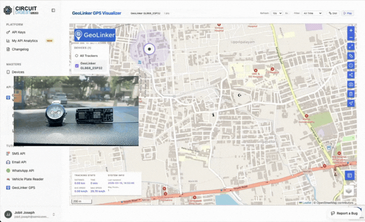
Also, if you are completely new here, GeoLinker is a GPS tracking and cellular monitoring cloud platform with both software and hardware stack from CircuitDigest. Basically, GeoLinker GPS visualizer is a free tool on CircuitDigest Cloud that allows you to store and visualise GPS coordinates on a neat map. GeoLinker also has hardware modules, like the GL868 ESP32 GSM/GPS module that comes with a M2M SIM IoT card and tons of other interesting features. That being said, let’s get back to our story of M2M IoT SIM cards.
What Exactly is an M2M IoT SIM Card?
An M2M (Machine-to-Machine) SIM card is basically a SIM card designed specifically for machines instead of human users. Unlike the SIM card inside your smartphone, these SIMs are meant for devices like GPS trackers, smart meters, industrial sensors, fleet monitoring systems, and other cellular IoT products.
The difference is not just in pricing. The entire network architecture around M2M SIM cards is different. Normal SIM cards are designed assuming a human is using the device for browsing websites, making calls, watching videos, and moving between towers constantly.
But IoT devices behave very differently. For example, a GPS tracker sitting inside a vehicle might only send a few kilobytes every few minutes. A remote sensor might wake up once an hour, upload data, and go back to sleep. Telecom operators treat these deployments differently, which is why M2M infrastructure exists in the first place.
Why Normal SIM Cards Become a Problem in IoT Projects
This is something most tutorials on the internet never really explain properly. Using a normal SIM card for a single prototype is fine, and most people still do it during early testing. But once the project becomes serious, where you want to keep it running 24x7 or scale it across multiple deployed devices, consumer SIM cards slowly become painful to manage.
The biggest issue is that consumer plans are not optimised for IoT usage at all. Imagine paying for 1 GB or 2 GB monthly plans when your actual device only consumes 100 MB. You are essentially paying for voice calls, entertainment bundles, and mobile usage patterns that your hardware will never use.
Then comes the operational side of things. Once you have multiple deployed devices, keeping track of recharges becomes frustrating. Some SIMs expire, some go inactive, and sometimes you discover a device stopped reporting simply because the recharge validity ended weeks ago. Debugging connectivity issues becomes difficult because you are never sure whether the problem is hardware, firmware, server-side, or simply the SIM itself.
We also noticed that some telecom networks behave differently when consumer SIM cards are continuously used inside GSM modules or embedded devices. Again, this is not usually a problem during prototyping, but for long-term deployments, it starts becoming unreliable. This is exactly the problem M2M IoT SIM cards are designed to solve.
Getting an M2M SIM Card in India is Surprisingly Difficult (Until Now)
After understanding the importance of M2M SIM cards, we decided that all GeoLinker boards should eventually be sold along with an M2M SIM card. And honestly, we assumed M2M SIM cards would be easy to obtain. We thought it would be similar to getting a corporate SIM connection or maybe a postpaid enterprise plan. It turned out to be much more complicated.
In India, M2M services are offered by major telecom operators like Bharti Airtel, Reliance Jio, and Vodafone Idea, but directly obtaining these SIM cards as a small company or startup is not straightforward at all.
Even today, if you search online for “M2M IoT SIM Card India,” you mostly end up finding random resellers, unclear IndiaMART listings, enterprise vendors with almost no documentation, and expensive industrial providers. The biggest problem is that nobody clearly explains the actual process.
After bumping around for quite some time, we finally found that we had to work directly with a telecom operator and register ourselves as an M2MSP (M2M Service Provider), after which we would become eligible to get M2M SIM cards and distribute them with our GeoLinker modules.
The SARAL and M2MSP Process
So yes, if you want to directly get M2M IoT SIM cards from telecom operators in India, you should be registered as an M2M Service Provider (M2MSP). And to become an M2MSP, you would need to register through the SARAL Sanchar Portal on the Department of Telecommunications website and obtain your SARAL number.
For this registration, your company should be a registered business in India, and you would typically need to submit a GST certificate, PAN card, Certificate of incorporation, MoA documents, Aadhaar, Company address proof on a company letterhead with seal and signature
After getting the SARAL number approved, you can register with a telecom operator to become an M2MSP. All this might sound easier said than done, but it took us almost 6 months for everything to be completed, so expect some delays if you are planning to go through the process yourself.
From there, you can raise a PO for the type of plans you need on your M2M SIM cards, get the SIM cards issued, activate them, and start using them with your IoT GSM modems. At least, that’s what we thought until we discovered whitelisting.
The Whitelisting Part Nobody Explains
This was honestly one of the most confusing parts when we first started using M2M SIM cards. With a normal mobile SIM, you can access almost anything on the internet without thinking twice. But M2M SIM cards often operate in a more controlled environment.
In simple terms, the SIM card may only allow access to whitelisted servers, domains, IP addresses, or services. Not just internet access, even to send an SMS or make a call from your M2M SIM card, you may have to whitelist the receiver’s number before it works.
At first, this feels restrictive, but after understanding the reason behind it, it actually makes sense. These SIMs are designed for industrial deployments where security and controlled communication matter much more than unrestricted browsing.
For large OEMs building thousands of devices, this is normal. They already know exactly which cloud server or backend infrastructure their device will communicate with. But for makers, startups, and developers experimenting with different platforms, this quickly becomes frustrating.
During development, you constantly switch between services like MQTT brokers, cloud dashboards, automation platforms, and testing servers. Managing whitelisting manually for every deployment becomes painful very quickly.
Why We Built GeoLinker Around This Problem
At some point, we realized we were spending more time solving telecom and deployment problems than actually building hardware. That frustration is honestly what led to GeoLinker.
GeoLinker is part of the CircuitDigest Cloud ecosystem and was built as a GPS tracking and cellular IoT platform that combines both hardware and cloud infrastructure together. Instead of treating connectivity as a separate complicated process, we wanted developers to simply power up a module and start building. That is where the GeoLinker GL868 came in.
The GL868 is an ESP32-based GPS tracking and cellular IoT module built around the SIMCom SIM868 modem. When you purchase the module, it is sold with an M2M IoT SIM card, along with 3 months of free data and voice plans (120MB/month | 200 SMS | 100 outgoing minutes) already included. You can check out the article on how to activate the GeoLinker M2M IoT sim card if you have already purchased a GeoLinker board and are interested in seeing how to activate the sim card and start building.
Since the SIM868 modem already supports GSM and GNSS functionality, the module can handle both cellular communication and location tracking together. Developers can use it for vehicle tracking, remote monitoring, asset tracking, telemetry, and general IoT applications without having to combine multiple separate modules together.
Making the Activation Process Simpler
One thing we wanted to avoid was forcing users through telecom-level paperwork just to test a hardware module with an M2M SIM card. So instead of making developers manually figure out activation workflows, the SIM onboarding process was simplified through the GeoLinker portal itself.
The activation flow is intentionally simple. Users receive the module with the M2M SIM card already included. They can then link the SIM with an existing phone number through OTP verification and activate it through the portal.
In most cases, activation happens within a few minutes or, at worst, a couple of hours. KYC can later be completed to continue long-term usage.
The goal here was not to hide the telecom process completely, because that is still required legally, but rather to remove unnecessary friction for developers trying to build and test products quickly.
Solving the Whitelisting Problem for Developers
One thing we quickly realized is that most developers do not want to spend days dealing with network whitelisting during prototyping. So we pre-whitelisted many commonly used IoT and cloud platforms on the network side itself.
This includes popular services like AWS IoT, Arduino Cloud, Firebase, Adafruit IO, ThingsBoard, Blynk, Google Cloud, IFTTT, and many other commonly used IoT platforms.
For custom deployments, users can also request additional domains or IPs to be approved after verification. Similarly, phone numbers for SMS and voice communication can also be managed through the platform.
Again, the idea here was simple: developers should spend more time building hardware and less time fighting telecom infrastructure.
Recharge Plans for M2M IoT SIM Cards
Just like prepaid SIM cards, IoT M2M SIM cards also have different plans that developers can select based on their requirements. But here is a small catch: these plans have to be pre-approved by the telecom operator before they can be activated.
This means that when you get M2M SIM cards from the telecom provider, you have to raise a PO and specify what plans are needed for those SIM cards. Only the plans mentioned there will be available for activation. However, once a SIM is active, you can later switch between supported plans whenever required.
The image below shows the Airtel M2M plans that can be used with M2M IoT SIM cards.
Another important thing to note here is that, as a registered M2MSP, you will get the M2M IoT SIM cards free of cost from Airtel. But as soon as you activate a SIM under a plan, billing starts from day one. These charges will be added to your account irrespective of whether the SIM is actively being used or not.
Once activated under a monthly plan, recurring deductions will continue automatically.
If you are an M2MSP, you can suspend a SIM card to avoid full charges, but even in the suspended state, you still have to pay around Rs. 10/month. If you want to completely stop charges, the SIM card has to be terminated by the M2MSP. Once terminated, the SIM becomes unusable and cannot be reactivated later.
How to use M2M IoT SIM Card - The Basics
For our GeoLinker range of boards, we are currently using Airtel M2M IoT SIM cards. A typical Airtel IoT SIM card looks like the one shown below.
On top of the SIM card cover, you will find the SIM Number and IMSI Number printed on it. On the actual SIM card itself, you can again find the SIM Number printed. Do note that these numbers should be kept confidential, and they should not be confused with the actual phone number of your M2M IoT SIM card.
For a typical consumer SIM card, the phone number is normally +91 followed by 10 digits. But for IoT M2M SIM cards, you may get a 13-digit number, and this phone number is usually assigned only after activation through the portal and is not printed anywhere on the SIM card.
If you have purchased our GeoLinker board with an M2M IoT SIM card, you can check out our separate article on how to activate an Airtel M2M IoT SIM card using GeoLinker.
Currently, all GeoLinker boards are sold with physical SIM cards from Airtel, but we also have plans to introduce MFF2 SIM cards (SIM cards in VQFN chip packages) and eSIM support with our future radio modules and boards.
Getting MFF2 SIM cards in India still remains slightly confusing for us, and eSIM support is currently limited to a few high-end radio modules from Quectel and Nordic Semiconductor, so that is something we will continue exploring in the future.
Whitelisting, Terminating and Plan Extension on GeoLinker Modules
If you are using the Airtel M2M IoT SIM card from GeoLinker, you get free data, calls, and SMS for the first three months. You can activate it by entering your IMSI number, shown on the SIM cover, along with your personal phone number and verifying the OTP as shown below.
After the SIM is activated, you will be able to use it immediately. However, within a week of activation, you have to complete the KYC process by submitting your ID proof and picture verification through the GeoLinker portal itself.
By default, all popular platforms are already whitelisted by us. If you want to whitelist a particular phone number to send SMS or make calls, you can do that through the GeoLinker dashboard as shown below.
After three months of usage, you will get a notification to recharge your SIM card and extend your plan, which again can be done directly from the GeoLinker dashboard itself. If there is no active recharge, your SIM card will eventually be terminated within a week.
FAQ
1. Can I use a normal SIM card for IoT projects? Yes, for basic prototyping, you can use a normal SIM card. But for long-term deployment, scalability, and industrial reliability, M2M IoT SIM cards are much better.
2. What is the difference between an M2M SIM and a normal SIM? M2M SIM cards are designed specifically for machine communication and industrial deployments, whereas normal SIM cards are optimised for consumer smartphone usage.
3. Why does M2M SIM require whitelisting? Whitelisting improves security, prevents misuse, and allows telecom operators to maintain controlled industrial-grade network access.
4. Can I use M2M SIM with ESP32? Yes. M2M SIM cards work well with ESP32-based GSM and cellular IoT modules.
5. Does the GeoLinker GL868 support GPS? Yes. The module supports GPS, GLONASS, Galileo, and BeiDou GNSS positioning.
6. Can M2M SIM cards send SMS and make calls? Yes. Depending on the selected plan, M2M SIM cards can support Data, SMS, Incoming calls, and Outgoing calls
7. Do I need SARAL registration to get M2M SIM cards? If you want to directly source M2M SIM cards from telecom operators in India, SARAL registration and M2MSP onboarding are generally required.
8. Where can I get M2M IoT SIM cards in India? You can either register directly with telecom operators as an M2MSP, Work with authorised providers or use integrated IoT ecosystems like GeoLinker that simplify onboarding and activation
Related GPS Tracking Projects
Explore these exciting GPS tracking and IoT projects originally built using 2G GSM modules. Now, with Circuit Digest’s M2M IoT SIM solutions, these projects can be upgraded with more reliable connectivity, easier deployment, and better support for real-world IoT applications.
Learn how to build a Raspberry Pi Pico GPS Tracker using the Neo 6M GPS module and SIM800L. This hands-on guide covers interfacing, real-time data logging, and API-based location updates
Learn how to build a GPS tracker using Arduino UNO, SIM800L GSM module, and NEO-6M GPS with GeoLinker. This DIY project offers real-time location tracking, historical
Learn how to use the A7672S 4G LTE GNSS module with Arduino for GPS tracking and IoT communication. This guide covers pinout, interfacing, AT commands, and HTTPS data upload.
In this tutorial, we are going to see how you can create a custom Graphical User Interface(GUI) using LVGL and our favourite Arduino IDE. You can use any kind of microcontroller for this project; the only thing you need to do is to include the right pins in the Arduino code. Here, I’m using an ESP32-C3 based smartwatch for the demonstration. This has a display, touch, controller and everything integrated inside, so we don't want to make any messy wiring. Whether you are a hobbyist building a home-automation dashboard or a product developer prototyping a wearable UI, mastering LVGL on ESP32 with Arduino is one of the highest-leverage skills you can add to your embedded toolkit.
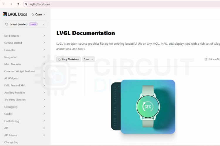
What Is LVGL? - Introduction to the Light and Versatile Graphics Library
LVGL stands for Light and Versatile Graphics Library, which is an open-source library that supports a wide variety of microcontrollers and displays. It’s a collection of components required to build a Graphical User Interface (GUI), mostly in embedded systems where custom UIs are needed. Examples include a Smart Home Automation & Monitoring Hub, a Desk32 Smart Hub for deep work focus, or even a Smart Wellness Clock that shows health metrics at a glance.
You will be able to see GUIs built on top of LVGL around you, like your smartwatch screens or display dashboards of some Attendance Systems in some offices. Developers use LVGL in a wide variety of ways, like some build GUIs using raw code while some others use some Drag-and-Drop visual editors like Square Line Studio or EEZ Studio that support LVGL. Here in this tutorial, we will use example code snippets provided by LVGL in their documentation to build a GUI out of it.
LVGL at a Glance
Feature
Detail
Full name
Light and Versatile Graphics Library
Language
C99 (C++ wrappers available)
License
MIT — free for commercial use
Minimum RAM
~32 kB (typical embedded target)
Minimum Flash
~128 kB
Supported MCUs
ESP32, STM32, RP2040, Arduino, NXP and more
Display interfaces
SPI, Parallel, RGB, MIPI-DSI
Visual editors
SquareLine Studio, EEZ Studio
Arduino library
Available in Arduino Library Manager
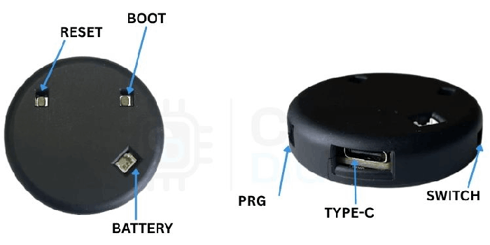
Hardware Used - ESP32-2424S012 Round Display Development Board
Let’s talk a little bit about the ESP32 C3 based development board that we use in this tutorial. First of all, it has an ESP32-C3 at its core. It has a 1.28” 240 * 240 round LCD display on top. The display uses the famous GC9A01 display driver, which is seen in many hobby-level round display modules. It uses the 7-pin SPI interface (SCL, SDA, DC, CS, RST, 3V3, GND) for communication. The touch IC used is CST816D. It has a battery charging IC, which is IP5306. You can use any display or controller for this tutorial; the only thing you need to do is modify the configurations to match your device.
What Do You Need Before Getting Started?
An ESP32-based development board that has either SPI or a parallel display connection.
Capacitive/Resistive Touch Controller – optional but strongly advised.
USB-C or Micro-USB cable for programming.
3.7V LiPo Battery – optional (in case of standalone functionality).
Software Prerequisites
Arduino IDE 2.x – download from Arduino.cc.
ESP32 board package – available on Arduino Boards Manager (https://raw.githubusercontent.com/espressif/arduino-esp32/gh pages/package_esp32_index.json).
LVGL for Arduino library – available from Arduino Library Manager ("lvgl").
Driver files of the display and touch controller - CST816D.h, CST816D.cpp – obtain from project GitHub repo.
Knowledge Prerequisites
Basic syntax of Arduino C++ code – setup/loop methods.
I²C/SPI protocol knowledge.
GPIO mapping knowledge of the ESP32 board.
ESP32-2424S012 Full Specifications
Model
ESP32-C3 1.28" IPS Round Display
ESP32 Series
ESP32-2424S012
Processor
ESP32-C3 is a Single-Core RISC-V
Display Driver
GC9A01
Touch Driver
CST816S
Frequency
up to 240MHz
Wi-Fi
Supports 2.4GHz
Display
1.28inch
Touch display
Capacitive
Resolution
240×240
Dimensions(D*H)
45.5*11mm
Weight
20g
You can power the module either via the Type-C connector that’s available on board or using a 3.7V LiPo battery by connecting it to the 2-pin JST connector in the back of the module.
Step-by-Step Setup: LVGL Arduino GUI on ESP32
Step 1 ⇒ Install the LVGL Library in Arduino IDE
You need to go to the Arduino Library Manager and search for lvgl. Install the latest release by kisvegabor.Now, you need to head over to the official documentation of LVGL.
Step 2 ⇒ Browse the LVGL Widget Documentation
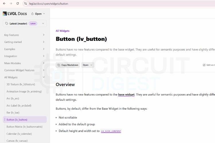
In this tutorial, we are going to build a simple switch project using LVGL and Arduino IDE. We can make this project in several different ways - meaning using LVGL and without using LVGL. From my experience, if we build a custom GUI using LVGL, we get a smartphone app kind of quality for the UI. This is because LVGL has a mature set of design components and animations that outperform any other competitors like TFT_eSPI. Now, let’s go to All Widgets > Button This opens the button widgets available in LVGL. You can see a lot of example widgets for buttons.
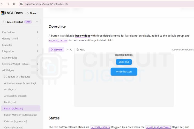
Let’s scroll down and go to the first example. You can see options for Preview - meaning see how the button functions, and Code - meaning see the code snippet for that particular button.
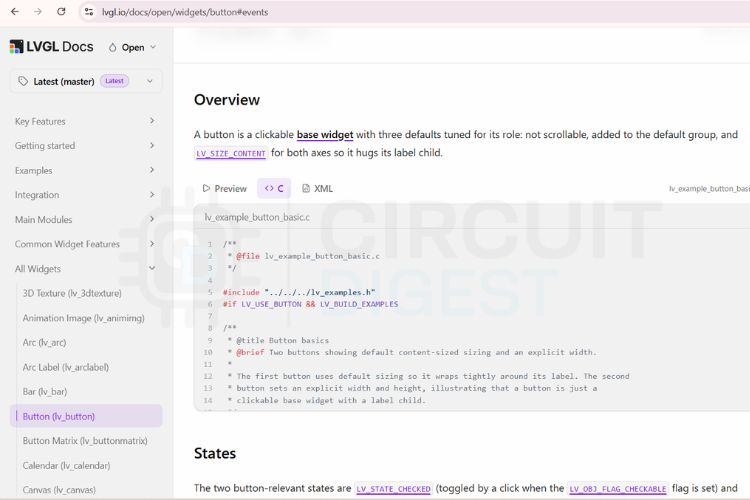
Step 3⇒ Copy the Code Snippet
Let’s open the code snippet part of the example, which reveals the code behind the preview.
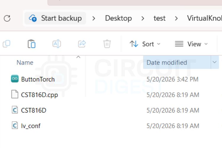
Step 4⇒ Understand the Project Folder Structure
Let’s copy the code from that section. If you check out the GitHub repo mentioned below, you will be able to download all the code for this project. You will be able to see three files along with the main Arduino code, as shown below.
You have the main Arduino code, then the LVGL configuration file named lv_conf and then the touch configuration files, which are CST816D.cpp and CST816D.h. For this tutorial, we just need to modify the main Arduino code with the code snippet that we just copied. You may need to modify the pin configurations as per your setup.
Step 5⇒ Paste the Snippet into the Arduino Sketch
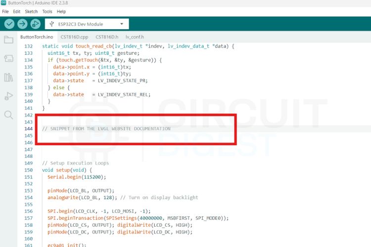
Once the Arduino code is opened, you can see a section asking for “SNIPPET FROM THE LVGL WEBSITE DOCUMENTATION”. Paste the code snippet in this section. This code now gives the same button transitions in the display as we saw in the preview in the documentation.
The modified code snippet is attached to the code provided on GitHub. Select the right board and right port in your Arduino IDE and hit the upload button.
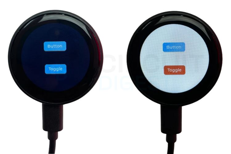
Step 7 ⇒ Test the Result Once the code is successfully uploaded, you can see the screen displaying the buttons exactly in the same way as shown in the preview in the LVGL documentation. You can see the button animations as well when you press the buttons. As we modified the code to change the screen background to white when the toggle button is turned on, you can see the background colour turning to white and black when we turn on and off the toggle button, as shown below. This is an excellent LVGL ESP32 project to study after completing the basic tutorial.
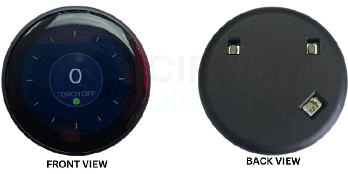
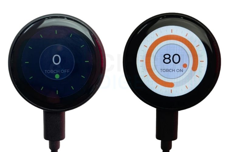
You can see another folder in the same repo named VirtualTorch. This project is shared for your future reference. It’s an advanced version of this tutorial that has a button for the torch and a slider around the button to adjust the brightness, too. Below are the two screens of the VirtualTorch project, before the button is pressed and after the button is pressed and the slider adjusted.
Code Explanation: How the LVGL Arduino Sketch Works
Above is the LVGL interface layer, which interfaces our hardware, the ESP32 display and touch with THE LVGL library.
5. Event Handler and Button Widget (LVGL Snippet)
static void event_handler(lv_event_t * e)
{
   lv_event_code_t code = lv_event_get_code(e);
   lv_obj_t * target = (lv_obj_t *)lv_event_get_target(e); // Get which widget was interacted with
   if(code == LV_EVENT_CLICKED) {
       Serial.println("Clicked");
   }
   else if(code == LV_EVENT_VALUE_CHANGED) {
       Serial.println("Toggled");
       // Check if the widget that fired the event is currently checked (turned ON)
       if(lv_obj_has_state(target, LV_STATE_CHECKED)) {
           // Toggle is ON -> Turn active screen background to White
           lv_obj_set_style_bg_color(lv_screen_active(), lv_color_white(), LV_PART_MAIN);
       } else {
           // Toggle is OFF -> Turn active screen background back to Black/Dark slate
           lv_obj_set_style_bg_color(lv_screen_active(), lv_color_hex(0x151525), LV_PART_MAIN);
       }
   }
}
void lv_example_button_1(void)
{
   lv_obj_t * label;
   lv_obj_t * btn1 = lv_button_create(lv_screen_active());
   lv_obj_add_event_cb(btn1, event_handler, LV_EVENT_ALL, NULL);
   lv_obj_align(btn1, LV_ALIGN_CENTER, 0, -40);
   lv_obj_remove_flag(btn1, LV_OBJ_FLAG_PRESS_LOCK);
   label = lv_label_create(btn1);
   lv_label_set_text(label, "Button");
   lv_obj_center(label);
   lv_obj_t * btn2 = lv_button_create(lv_screen_active());
   lv_obj_add_event_cb(btn2, event_handler, LV_EVENT_ALL, NULL);
   lv_obj_align(btn2, LV_ALIGN_CENTER, 0, 40);
   lv_obj_add_flag(btn2, LV_OBJ_FLAG_CHECKABLE);
   lv_obj_set_height(btn2, LV_SIZE_CONTENT);
   label = lv_label_create(btn2);
   lv_label_set_text(label, "Toggle");
   lv_obj_center(label);
}
Above is the snippet that we copied from the LVGL Documentation. It has two parts or two functions. First is an event_handler(), which is the UI part of the snippet. It builds the two buttons using the same widget template that we chose from the documentation.
6. setup() - Hardware and LVGL Initialisation The second part is the lv_example_button_1(), which performs the whole logic of the two buttons.
This is the setup() loop that fires exactly once when the device boots. It initialises the hardware in a sequential order, like turning on the display backlight, then initialising the display engine, then the touch.
Check TP_SDA / TP_SCL defines; ensure touch.begin(); is inside setup()
lv_conf.h: No such file or directory
lv_conf.h missing from sketch folder
Copy lv_conf_template.h to the sketch folder, rename to lv_conf.h, set #if 1
Sketch too big / out of flash
Unused LVGL widgets are consuming flash
Disable unused widgets in lv_conf.h: #define LV_USE_CHART 0
Display colours wrong/ inverted
Incorrect colour format setting
Try LV_COLOR_FORMAT_RGB565 instead of LV_COLOR_FORMAT_RGB565_SWAPPED
Touch coordinates mirrored
Display and touch orientation mismatch
Swap X/Y or negate the axis in touch_read_cb()
LVGL vs TFT_eSPI
Factor
LVGL
TFT_eSPI
Widget system
Full widget library (buttons, sliders, charts…)
None — manual drawing only
Animation engine
Built-in, hardware-accelerated
None built-in
Touch input handling
Built-in input device abstraction
Manual polling required
Memory overhead
Higher (frame buffer + widget tree)
Lower
Learning curve
Moderate (port layer setup required)
Low (simple API)
UI quality ceiling
Smartphone-grade
Basic / custom shapes
Visual editors
SquareLine Studio, EEZ Studio
None
Best for
Product UIs, dashboards, wearables
Simple graphics, gauges, fonts
Arduino LVGL GitHub
Explore open-source Arduino and LVGL projects on GitHub to build modern embedded GUI applications with touch-enabled displays. Find libraries, sample interfaces, and hardware integration examples that simplify creating responsive and visually rich IoT dashboards.
Conclusion
From this tutorial, we came to understand how to properly use the free and open-source graphical library called LVGL, which is used to develop GUIs for embedded systems. We can use our own hobby-level microcontrollers like the ESP32 or similar ones to run such programs. The future is endless, you can create your own embedded systems projects, home automations or any other projects requiring custom GUIs. You can refer to the codes provided in the GitHub repo for any future references. If you would like to see how we can implement LVGL in a real-life project, check out our Voice-Activated LED Controller using ESP32S3 project. For inspiration, take a look at how display-based interfaces can be applied in a radar-based human presence and fall detection system, a great example of combining sensor data with a meaningful on-screen interface.
Frequently Asked Questions
⇥ Why is LVGL used with Arduino? The LVGL (Light and Versatile Graphics Library), which is an open-source C library for developing touch-interactive GUIs on microcontrollers, can be used with Arduino, as it integrates well with the Arduino platform; is compatible with the ESP32 and many other popular boards; and produces smartphone-quality animations and widgets without a separate GPU.
⇥ Can I use LVGL with Arduino IDE? Yes, LVGL works with Arduino IDE. You just need the LVGL Library installed.
⇥ What is lv_conf.h? lv_conf.h is the LVGL configuration file.
⇥ Why do we need CST816D.cpp and CST816D.h? These files are the touch controller driver. They help the ESP32 communicate with the CST816D touch IC using I2C.
⇥ Which communication protocols are used here? SPI for display communication, I2C for touch communication and UART for serial programming.
⇥ Can I use another display instead of GC9A01? Yes, you only need the correct display driver and pin configurations of your display.
⇥ Can I make custom UIs instead of using widgets? Yes, LVGL allows custom drawing, animations, gradients, gauges, etc...
Touch-Based GUI Projects
Explore interactive touch-enabled GUI projects built using modern microcontrollers and display modules for smart control, automation, and real-time monitoring applications. These projects demonstrate intuitive user interfaces with responsive controls, animations, and sensor integration for a seamless embedded experience.
MATLAB can perform many advanced image processing operations, but for getting started with Image processing in MATLAB, here we will explain some basic operations like RGB to Grey, rotating the image, binary conversion, etc.
At the end of this project, we will create a very basic GUI using which we can set an alarm and when the alarm goes off, we will have a voice which tells us the current time and day with some pre-defined text. Sounds cool, right!! So let us build one.
If your Raspberry Pi IP address static configuration is changing too often, this complete guide is going to demonstrate how to configure a Raspberry Pi to use static IP through NetworkManager (using nmcli) and desktop GUI methods.
At Electronica 2026, while exploring the Silicon Labs booth, I came across a wireless networking technology that was surprisingly new to me, Wi-SUN. As embedded engineers, most of us are already familiar with technologies like BLE, Zigbee, Matter, Thread, and LoRa when it comes to IoT connectivity.
At a recent community webinar focused on building robotics companies in India, Raghvendra Sutar, founder of Kikobot, discussed how he started the company, the products it has developed, the challenges of manufacturing robotics hardware, and the company’s plans to expand into industrial robotics.
Adviteey Mehaindroo, the founder and CEO of Zinikus, credits CircuitDigest as one of his earliest learning grounds. Now he's sitting down with the same platform, talking about running a robotics company with a half-million-dollar valuation. He describes Zinikus as “a robotics company focused mainly on humanoids, but also catering to the advertising and hospitality sectors with robotics.”
As I sit down to write this piece, I notice the fan whirring above and, for the first time, it occurs to me that it runs on an induction motor. So does every other fan in my office and my home. These motors have been around for a long time, not because they’re the best options out there, but because they’re cheap and do the job. BLDC motors have gained a bit of popularity, but are pricier and usually come with an import dependency problem.