If you're after a reliable timing option for your next electronics project, the CD4047 multivibrator IC can provide the solution you need. Whether you need a CD4047 inverter circuit for power conversion or the more accurate CD4047 astable multivibrator circuit used in timing applications, this guide covers it all from the basic CD4047 pin diagram to more sophisticated CD4047 circuit diagrams!
In this article, we will delve into the fascinating world of the CD4047, exploring its functionality and practical applications in an easy-to-understand manner. We'll cover both hardware implementation and Proteus simulation to illustrate its effective use.
Quick Overview
Duration: 2-3 hours | Type: Circuit Theory | Difficulty: Beginner-Intermediate
Technical Scope:
Multivibrator circuits, timing calculations
Use Cases:
Inverters, timers, signal generation
What is CD4047?
The CD4047 is a CMOS-based multivibrator IC that generates precise timing signals in both astable and monostable modes. Key features include:
- Voltage range: 3V to 20V operation
- Power consumption: Ultra-low 2µA typical
- Operating modes: 6 different configurations
- Applications: Inverter circuits, timers, square wave generation
- Package: 14-pin DIP and SMD available
Before diving into practical CD4047 circuit diagrams, let's understand the CD4047 pin diagram and specifications that make this IC so versatile for both beginners and professionals.
CD4047 Pin Diagram and Pinout Configuration

The image above shows the pinout of the CD4047, providing a clear explanation of each pin. Further, the pin description of CD4047 is explained in the table below
Pin No | Pin Name | Description |
1 | C | Used to connect External Capacitor |
2 | R | Used to connect External Resistor |
3 | R-C COMMON | Common Pin for the externally connected Resistor and Capacitor |
4 | A͞S͞T͞A͞B͞L͞E͞ | Used as a Trigger Input, only for the Complement Gating Function, OtherWise kept HIGH |
5 | ASTABLE | Used as a Trigger Input for Astable Modes, otherwise kept LOW |
6 | -TRIGGER | Used as a Trigger Input, Only for Negative Edge Trigger Mode, Otherwise kept LOW in the case of Monostable Functions or HIGH in the case of Astable Functions |
7 | VSS | Negative Supply Voltage |
8 | TRIGGER | Used as a Trigger Input for Monostable Modes, Otherwise Kept LOW |
9 | EXTERNAL RESET | A Positive Pulse Resets the Q and Q̅ State to LOW and HIGH Respectively |
10 | Q | Output |
11 | Q̅ | Inverted Output |
12 | RETRIGGER | Used as a Trigger Input For Retriggerable Function, else kept LOW. |
13 | OSC OUT | Oscillator Output |
14 | VDD | Positive Supply Voltage |
Quick Reference: CD4047 Technical Specifications
The table below presents some quick specifications that you should be aware of. Let's discuss them briefly! These specifications are essential to designing dependable CD4047 circuits. Keep in mind the voltage limits and range of component values when designing your CD4047 inverter circuit or any timing applications.
| | Limits | Limits | Limits | |
Parameter | Symbol | Min | Typ | Max | Unit |
DC Supply Voltage Range | VDD | 3 | 15 | 20 | v |
Operating Current | IDD | - | 2 | 200 | µA |
Input Voltage High (VDD = 5V, VOH > 4.5V, VOL < 0.5V) | VIH | 3.5 | - | - | v |
Input Voltage Low (VDD = 5V, VOH > 4.5V, VOL < 0.5V) | VIL | - | - | 1.5 | v |
Input Voltage High (VDD = 15V, VOH > 13.5V, VOL < 1.5V) | VIH | 11 | - | - | v |
Input Voltage Low (VDD = 15V, VOH > 13.5V, VOL < 1.5V) | VIL | - | - | 4 | v |
DC Input Current, All Inputs | - | - | ± 10 | - | mA |
Operating Temperature | TA | -55 | - | 125 | °C |
Storage Temperature | TSTG | -65 | | 150 | °C |
Lead Temperature During Soldering | - | - | - | 265 | °C |
Firstly, take note of the Operating Voltage. This IC can operate with a minimum voltage of 3V and a maximum of 20V. However, for optimal stability in terms of power dissipation and oscillating frequencies, recommended operating voltages are 5V, 10V, and 15V. Regarding Current Consumption, since this IC is designed for low-power operation, it typically ranges from 2µA to a maximum of 200µA.
Next, let's consider Input and Output Voltages, which depend on VDD and VCC. For instance, with a supply voltage of 5V, a voltage below 0.5V is considered LOGIC LOW, while a voltage between 0.5V and 4.5V (or up to VDD) is considered LOGIC HIGH.
Unlike some other ICs, this IC is available in various variants with different Operating Temperatures to suit specific needs. Choose the variant that best fits your requirements. The top variant operates at a temperature of around 125°C. When soldering, be cautious not to overheat the IC's leads beyond 265°C to prevent internal damage. For more detailed information, refer to the official datasheets available online.
Now that you understand the CD4047 pin diagram, let's explore how different pin configurations create various operating modes. These CD4047 circuit diagram variations enable astable, monostable, and specialised timing functions.
CD4047 Circuit Diagram: Operating Modes and Configurations
The CD4047 primarily offers two main functions: Astable Multivibrator and Monostable Multivibrator. Within these functions, there are 3 modes for Astable operation and 4 modes for Monostable operation, as shown in the image below:

You might be wondering about how to switch between these modes. Don’t panic—switching between these modes is made simple using the table below
| TERMINAL CONNECTIONS | TERMINAL CONNECTIONS | TERMINAL CONNECTIONS | |
FUNCTION | TO VDD (+ve) | TO VSS (-ve) | INPUT | PULSE OUTPUT |
ASTABLE MULTIVIBRATOR | | | | |
Free Running | 4, 5, 6, 14 | 7, 8, 9, 12 | - | 10, 11, 13 |
True Gating | 4, 6, 14 | 7, 8, 9, 12 | 5 | 10, 11, 13 |
Complement Gating | 6, 14 | 5, 7, 8, 9, 12 | 4 | 10, 11, 13 |
MONOSTABLE MULTIVIBRATOR | | | | |
Positive Edge Trigger | 4, 14 | 5, 6,7, 9, 12 | 8 | 10, 11 |
Negative Edge Trigger | 4, 8, 14 | 5,7, 9, 12 | 6 | 10, 11 |
Retriggerable | 4, 14 | 5, 6, 7, 9 | 8, 12 | 10, 11 |
External Countdown | 14 | 5, 6, 7, 8, 9, 12 | - | 10, 11 |
By following the terminal connection table provided above, you can easily set the respective modes. The external capacitor and resistor pins remain the same for every mode; only their values might change according to specific needs.
Regarding the outputs, there are three pins: Q, Q̅ (Q-bar), and Oscillator Out. Q is the main output, Q̅ is the complement output of Q, and Oscillator Out is a direct output from the Astable Multivibrator block of the IC. The Q and Q̅ outputs come from the frequency divider block, which divides the frequency by two.
Let's delve into the modes of operation of the CD4047, starting with the Astable Multivibrator mode. Among the available three modes (Astable, Monostable, and Bistable), we will begin with a detailed explanation of the Astable Multivibrator mode. We'll cover Free Running mode briefly and discuss its stimulation.
Following that, we'll explore the Monostable Multivibrator mode, which offers four distinct modes. In particular, we will focus more on the Positive Edge Trigger mode within the Monostable Multivibrator configuration, providing a deeper understanding of its operation and applications.
The CD4047 astable multivibrator circuit is perfect for continuous square wave generation. Regardless of assembling a CD4047 inverter circuit or requiring accurate timing signals, these circuits ensure astable oscillation.
CD4047 Astable Multivibrator Circuit: Free Running Mode
In simple terms, an Astable Multivibrator is a circuit that generates a continuous output oscillating between two states, typically producing a square wave (Q) as shown in the figure below.

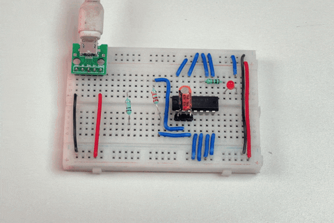
This square wave finds numerous applications in digital electronics. The below gifs show the CD4047 working in Astable mode. We have used an LED to provide a visible Output of the generated continuous square wave. You can notice that the LED turns on when the square wave is high and turns off when the wave is low. Here, the Q was the Square wave generated by the 10th Pin, and that's where the LED is connected. OSC is the Oscillator Output, which was not used in the above setup.
As previously mentioned, the CD4047 offers 3 modes within astable operation. Let's discuss each mode separately in detail
CD4047 Astable Multivibrator Circuit: Free Running Configuration
In Free Running Mode, a series of square waves is continuously generated whenever the system is powered up. In this mode, we can adjust the frequency of the oscillated output while the circuit operates autonomously.

The above circuit diagram depicts the Free Running mode configuration of the CD4047 IC. Here's a breakdown of the connections:
- Pins 4, 5, 6, and 14 are connected to the positive supply voltage (+5V).
- Pins 7, 8, 9, and 12 are connected to the negative supply voltage (Ground/Gnd).
- A 10uF capacitor is connected between Pins 1 and 3.
- A 22KΩ resistor is connected between Pins 2 and 3.
- An LED is connected to the 10th Pin (Q) along with a current-limiting resistor of 220Ω.
For simulation purposes, an oscilloscope is connected to Pins 10 (Q output), 11 (Q̅ output), and 13 (OSC output) to observe the waveform outputs and timing characteristics of the CD4047 in Free Running Mode. This setup allows for visualising the oscillation behaviour and waveform generation of the circuit.

CD4047 Frequency Calculator: Getting Timing Formulas Right. Correct timing calculation is important for effective CD4047 circuit design. You can use these formulas with our recommended component values to get accurate frequencies in your projects.
This part of the calculation remains the same for all the Modes in the Astable Multivibrator
The timing (tA) is calculated using the formula:
tA = 4.40 x R x C
For example, using a chosen capacitor of 10µF and a resistor of 22KΩ:
tA = 4.40 x 22K x 10µF
= 0.968 sec
So, approximately, it can be considered as 1 second. Remember, tA represents the timing of the full cycle. To determine the half-cycle time, simply divide tA by two.
The ideal waveform was provided above for your reference. There is no Trigger Signal, as powering up the circuit itself starts the oscillator. Here, Q was the actual output, and Q̅ was the Inverted Output. OSC was the internal Astable oscillator’s direct output. So, technically, the Q and Q̅ were the output from the internal frequency divider, which divides the frequency by two. These square waves are generated continuously at the predefined frequency with the help of R and C.
Stimulation of Free Running Astable Multivibrator:
As per the circuit diagram of Free Running mode explained above, the circuit was replicated in Proteus for stimulating the CD4047 in Free Running Astable Multivibrator Mode.

The above was the simulation result of a free-running astable multivibrator. Here, the expected pulse interval was calculated as tA = 4.40 × 10 µF × 22 kΩ = 0.968 seconds. However, in the simulation above, we obtained a result closer to 1.1 seconds, which was quite acceptable. We also created a prototype on a breadboard and achieved the expected result.
However, it's important to note that in the real world, there are many factors that can affect timing. Therefore, fine-tuning your circuit to achieve a precise frequency can be quite challenging!
True Gating Mode in Astable Multivibrator
As in the free running mode, a series of square waves are generated, but with the condition that it requires a trigger signal.

The above circuit diagram of the True Gating Mode configuration of the CD4047 IC. Here's a breakdown of the connections:
- Pins 4, 6, and 14 are connected to the positive supply voltage (+5V).
- Pins 7, 8, 9, and 12 are connected to the negative supply voltage (Ground/Gnd).
- A 10uF capacitor is connected between Pins 1 and 3.
- A 22KΩ resistor is connected between Pins 2 and 3.
- An LED is connected to the 10th Pin (Q) along with a current-limiting resistor of 220Ω.
- The 5th pin (ASTABLE) is intended to be an input here. It is connected to 5V via a push button and pulled down via a 10KΩ resistor.

The square waves are produced only when the Trigger pin is kept HIGH. If the Trigger pin is LOW, the oscillator remains turned OFF. You can see this in the above Ideal Graph. Here, if the pulse width of the Trigger input was lower than tA, the Output will be held ON for the first cycle of Oscillations as shown above.
Complement Gating - Astable Multivibrator
Complement Gating is similar to True Gating, as the name implies. In Complement Gating, the oscillator is turned on by an active LOW signal and turned off by an active HIGH signal. To achieve this operation, a slight change in the circuit connection is required.

The circuit was the same as the true astable gating, but with only one difference. Here, the 4th pin ( A͞S͞T͞A͞B͞L͞E͞ ) served as the trigger input. This pin was connected to ground via a push button and pulled up via a 10 kΩ resistor. So, the 5th Pin, along with Pins 8, 9, 12, was Connected to the Negative Power Supply (GND or Ground)

Like the circuit, the above ideal graph was very similar, with only one difference: the trigger signal appears inverted.
So with this, we are completing the Astable Multivibrator modes. Next, let's explore the Monostable Multivibrator and its modes.
While astable circuits continuously oscillate, CD4047 monostable circuits offer single-shot timing with high precision. These timer arrangements are perfect for delay circuits, pulse stretching, and time-controlled circuits.
CD4047 Monostable Circuit: Timer Applications and Modes
As the name implies, the Monostable function has only one stable state, which changes to an unstable state when an external trigger is applied. After a fixed period, it returns to the original stable state. This functionality is commonly used as a timer in various applications. While modern microcontrollers are more capable than this simple IC, the CD4047 excels in speed, efficiency, reliability, and cost for specific tasks.
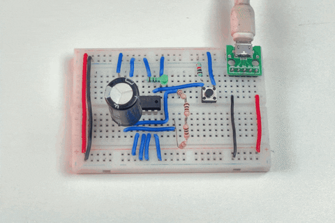
The following GIF demonstrates the CD4047 operating in Monostable Multivibrator Mode. In this setup, a push button is used to trigger the timer, and an LED is used to indicate the output visually.
Below is a graph representing the basic output waveforms of the Monostable Multivibrator. The TRIG waveform is generated when pressing the push button, and the Q waveform represents the output from the 10th Pin (Q), where the LED is connected.

Next, let's begin with an introduction to the calculation part of the Monostable Multivibrator.
This part of the calculation remains the same for all modes in the Monostable Multivibrator.
The timing (tM) is calculated using the formula:
tM = 2.48 x R x C
For example, using a chosen capacitor of 1000µF and a resistor of 400Ω:
tM = 2.48 x 400 x 1000µF
= 0.992 sec
So, approximately, it can be considered as 1 second.
Now, let's delve into the operating modes of the Monostable Multivibrator, starting from the Positive Edge Trigger Mode.
CD4047 Monostable Circuit: Positive Edge Trigger Configuration
The Positive Edge Trigger is simpler to understand in its basic operation as a timer. When the trigger push button is pressed, the output is held high for a specific amount of time and then pulled low. This is the primary application of this configuration.

The above circuit diagram depicts the Positive Edge Trigger Mode configuration of the CD4047 IC. Here's a breakdown of the connections:
- Pins 4 and 14 are connected to the positive supply voltage (+5V).
- Pins 5, 6, 7, 9, and 12 are connected to the negative supply voltage (Ground/Gnd).
- A 1000uF capacitor is connected between Pins 1 and 3.
- A 400Ω resistor is connected between Pins 2 and 3.
- An LED is connected to the 10th Pin (Q) along with a current-limiting resistor of 220Ω.
- Pin 8 (+TRIGGER) was connected to Positive Supply voltage via push button and Pulled Down Via 10kΩ
For simulation purposes, an oscilloscope is connected to Pins 8 (+TRIGGER), 10 (Q output), 11 (Q̅ output), and 13 (OSC output) to observe the waveform outputs and timing characteristics of the CD4047 in Positive Edge Trigger Mode.

While the resulting waveform may resemble that of a true gating astable multivibrator, the key distinction lies in the trigger mechanism. In a monostable multivibrator, if the trigger is pressed continuously for an extended interval, the output is driven high for a fixed duration and then automatically turned off. Conversely, in true gating mode, the output remains continuously high as long as the trigger input is maintained in a high state.
Here, the Trigger pulse is responsible for Switching ON and OFF the Internal Oscillator.
Stimulation of the Positive Edge Trigger in Monostable Multivibrator:
The circuit diagram for the Positive Edge Trigger mode was replicated in Proteus for simulation. As you know, a push button connected to the 8th pin of the CD4047 served as the trigger input, and an LED connected to the 10th pin (Q) of the CD4047 was used as the output indicator. One important thing to remember is that if you want to visually observe the output via the LED, ensure that the calculated pulse width is at least greater than 300 ms; otherwise, it will be too fast to notice.

The above was the simulation of a Positive Edge Trigger Monostable Multivibrator. We also created a prototype on a breadboard and achieved the expected result.
Please note that there will be slight differences between simulation and real-world prototypes due to factors such as component tolerances. Therefore, you may need an oscilloscope or frequency measuring device to fine-tune the output pulse width. Use potentiometers instead of fixed resistors for easier tuning. Once tuning is completed, you can replace the potentiometer with a static resistor by measuring the actual resistance in the potentiometer.
Negative Edge Trigger Mode in Monostable Multivibrator
It is similar to the positive edge trigger, but in this case, the system is activated by an active LOW signal, which initiates a delay in the circuit.

To enable Negative Edge Trigger Mode, connect the trigger input to the 6th Pin (-Trigger) with a pull-up configuration, and connect the 8th Pin (+TRIGGER) to the positive supply voltage (5V). The rest of the circuit remains the same as in the Positive Edge Trigger Mode.

This graph was similar to Positive Edge Trigger mode, as the functions are essentially the same except for the inverted trigger input. You may notice that there was only one rising edge in the oscillator output because after one cycle, the internal astable oscillator was turned off.
Retriggerable Mode in Monostable Multivibrator
This mode is particularly special because it can be utilised to extend the duration of the output pulse. Additionally, it can be employed to compare the frequency of an input signal with that of the internal oscillator.

In this setup, the connection is similar to a positive edge trigger with one modification: the 12th Pin (RETRIGGER) is combined with the 8th Pin (+TRIGGER), meaning both pins receive the same input pulse simultaneously. Therefore, there is no need for individual pull-down resistors. A common pull-down and a common push-button input are sufficient.

The above graph depicts the ideal behaviour for the Retriggerable Mode. In this mode, there is a feature that allows increasing the pulse width by using multiple trigger pulses. From the graph, it's evident that if the push button is pressed once, the pulse interval is 1tRE. If pressed twice, it's 2tRE, and so on. With continuous pressing, the output pulse will remain on indefinitely.
Unlike others, the Retriggerable Mode has a separate calculation, which will be discussed below.
Calculation of Pulse Width Of Retriggerable Mode:
It is the same as the main formula tM = 2.48 x R x C, with slight modifications due to the introduction of a new variable n representing the number of input pulses.
So, the time delay of a retriggerable monostable multivibrator (tRE) can be defined as follows:
tRE = (2.48 x R x C) x n
For example, using a chosen capacitor of 1000µF and a resistor of 400Ω and considering a two-pulse input,
tRE = (2.48 x 400 x 1000µF) x 2
= 1.984 sec
So, approximately, it can be considered as 2 seconds.
External Counter Mode in Monostable Multivibrator
This mode is considered to be an additional feature that requires an external IC to serve as the trigger input signal. It is somewhat similar to the Retriggerable mode, but instead of using a simple push button, an external digital signal is utilised.

The External Counter option enables extending the time duration of the output pulse beyond the intrinsic limits of the CD4047. By utilising an additional counter IC in combination with the CD4047, precise digital control over the output pulse duration can be achieved. This method enhances flexibility and accuracy in pulse timing applications.
Due to its unique ability, it has a distinct calculation method, which will be discussed below.
Calculation of Pulse Width of External Counter:
Here, the formula for calculating the pulse duration (tEC) looks like this,
tEC= (N - 1) (tA) + (tM + tA/2)
Where,
tEC - Pulse width of External Counter Mode
N - Number of Counts Set by the External Counter Circuitry
tA - period of the Internal Oscillator
tM– Desired period
(N-1) x tA -> Represent the total time taken for N cycles of the internal oscillator.
(tM + tA /2) -> Represents the additional time extended by the external circuitry
Finally, let's move on to our last topic, which covers limitations of timing components, including the range of values for R (resistors) and C (capacitors) that can be utilised, and more.
Timing Component Limitations
- It is recommended to use non-polarised capacitors with low leakage for optimal performance with the CD4047.
- There are no strict upper or lower limits for either the resistance (R) or capacitance (C) values to maintain oscillation.
- Based on internal calculations and practical considerations, the recommended values for R and C are as follows:
Capacitance (C):
- For astable modes: From 100 pF to any practical value.
- For monostable modes: From 1000 pF to any practical value.
Resistance (R):
- Minimum value: 10 kΩ
- Maximum value: 1 MΩ
Below are some of the Projects that you can try with CD4047:
1) Square Wave Generator Circuit using 4047 IC
Know how to generate a square wave using the CD4047's Astable Mode of operation, and as a bonus, learn how to convert the produced square wave to a sine wave.
2) 12v DC to 220v AC Inverter Circuit
Learn to create a simple inverter that converts 12V DC to 220V AC using CD4047 and a couple of MOSFETs.
CD4047 Applications & Uses
- Inverter Circuits: DC to AC conversion for power applications
- Timer Circuits: Precise delay and timing control
- Square Wave Generation: Clock signals and digital circuits
- Electronic Ballasts: Fluorescent lamp drivers
- Pulse Width Modulation: Motor control and power regulation
Frequently Asked Questions on the CD4047 Inverter Circuit
⇥ What is the CD4047 IC used for?
CD4047 is a CMOS-based multivibrator IC used for generating precise timing signals, square wave generation, inverter circuits, electronic ballasts, and timer applications in both astable and monostable configurations.
⇥ How do you find the frequency for a CD4047?
For Astable Mode, f = 1/(4.40 × R × C). For Monostable Mode, t = 2.48 × R × C. Using recommended values, R should be 10kΩ-1MΩ, and C can be 100pF (astable) or 1000pF (monostable).
⇥ What is the pin configuration of CD4047?
The CD4047 has 14 pins, VDD(14), VSS(7), C(1), R(2), R-C Common(3), Q(10), Q̅(11), OSC OUT(13), TRIGGER(8), -TRIGGER(6), ASTABLE(5), ASTABLE̅(4), RETRIGGER(12), EXTERNAL RESET(9).
⇥ Will a CD4047 work as an inverter?
Yes, the CD4047 is capable of producing square waves at the inverter circuit inputs. CD4047 in astable mode generates continuous oscillation, and the square waves can be utilised to drive transformers or MOSFETs to convert the DC voltage to AC voltage.
⇥ What is the distinction between astable mode and monostable mode in CD4047?
When in astable mode, the circuit goes on oscillating between two states, like high voltage and low voltage, producing square waves. Monostable mode, however, possesses one stable state and is switched to an unstable state for a predetermined time duration, and then comes back to the stable state.
⇥ What are the restrictions on the operating voltage of CD4047?
CD4047 works from a minimum of 3V to a maximum of 20V. CD4047 works mostly at voltages of 5V, 10V, and 15V for the best stable output. The amount of current drawn goes from a minimum of 2uA (microamp) to a maximum of 200uA (microamp).
Advance your skills with a deeper dive into analog signal generation and waveform control. These related projects walk you through designing classic multivibrators and waveform generator circuits using op-amps.
Astable Multivibrator Circuit Using Op-amp
In this project, we are going to build a simple Astable Multivibrator using Op-amp, and we will look at all the necessary calculations to find out the period hence we can calculate the frequency and duty cycle of the circuit.
Sawtooth Waveform Generator Circuit
In this tutorial we will show you, how to design a sawtooth wave generator circuit with adjustable gain and DC offset of the wave, using Op-amp and 555 timer IC.