
PCB Design

|
DIY ESP32 Oscilloscope The oscilloscope is a must-have test instrument for any electronics engineer. It is used to visualize and observe various signals, usually as a two-dimensional plot with one or more signals plotted against time. They are used in designing and debugging electronic devices to view and compare waveforms, and determine voltage levels, frequency, noise, and other… |

|
Design a 12V/27W SMPS Circuit with UC3843 SMPS Controller IC Switching Mode Power Supply, or simply SMPS, is a type of Power Supply Unit (PSU) that uses a switching device (such as a transistor or MOSFET) to convert the source, which can be AC or DC, to a constant DC voltage. Switched-mode power supply circuits (SMPS) are most often required in many electronic designs to convert the AC mains voltage to a suitable level of DC voltage… |

|
An Overview of Layer Stack Management in PCB Design When it comes to designing complex high-density PCBs, layer planning is important for different types of applications. Poor PCB layer stackup management contributes to the poor PCB design and ultimately cause the PCB to malfunction. Layer stackup is a process where lots of things are merged in a simple but calculative way into a single PCB design. To understand layer… |

|
Why do we need Differential Pair Routing and How can you use it for your next PCB Design? When you think about a PCB (Printed Circuit Boards) in general you can say it’s a piece of a board made out of fiberglass in which small and complex connections are etched with copper, but after designing hundreds of PCBs, I can tell you its a sophisticated piece of art where a perfectly designed circuit diagram is born, to become a part of the real world. A circuit or… |

|
Understanding Impedance Matching in PCB Design with Example and Calculation It is fair to consider a PCB itself as a component in which multiple traces are connected. Each trace is different, some are high speed, some are low speed, some are noisy, some are used by the return path of circuit current, etc. Now, as we all know, there are lots of variations in ideal circuits and real circuits. Suppose a high-frequency trace is routed with a 7mm copper… |

|
Simple Design Techniques that could Reduce your PCB Manufacturing Cost When you are designing and producing a product, a PCB can easily become one of the most costly components of the whole product, thus lowering the PCB cost can be one of the major factors that can be proven beneficial for lowering the overall production cost. Majorly, the PCB cost can be reduced by cutting the PCB size as well as selecting the proper components, and… |

|
How can Efficient Placing of Thermal Vias Improve Heat Management in PCB Designs? While designing a PCB, there are a lot of instances where we need to dissipate heat from certain components (Linear voltage regulator for example). In most cases, those devices are generic through-hole components, thus heat sinks effectively distribute the heat inside the area of Aluminium and keep the device in cooler ambient conditions. But if we are talking about any SMD… |

|
Here is why you should use Via Stitching for your next PCB Design There are multiple instances where a well-designed circuit has failed in the POC stage or in the Production Stage because of a bad PCB design. PCB design is an art where all components sit together and the connections are done via copper traces. It may seem to be an easy job to connect all but is rather a difficult task as different things of the… |
|
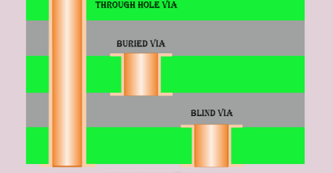
Understanding Blind, Buried, and Through-hole vias in PCB In a printed circuit board (PCB), via is a simple copper plated hole that connects one layer to another layer. In a generic double-sided PCB, via connects the top layer to the bottom layer, which is called through-hole vias. Vias are just drilled holes that are plated with copper in a PCB, and due to advancement in technology and precision machinery, we can… |

|
How can Teardrops help in Improving Quality and Stability of your PCB Design If you have been into PCB design and manufacturing for a long time, you would have probably come across some unexpected problems during the fabrication/manufacturing process. One among those problems is misaligned holes which will make the tracks of your PCB separate over time. By including teardrops in PCB, you can increase the overall quality and stability of the PCB, in… |

|
What are the Steps involved in Manufacturing a Flexible PCB? With the emergence of flexible PCB technology, modern electronic gadgets have come a long way. They are found in the core of many sensitive and delicate electronic products. Even your smartphone, camera, laptops, calculators, and many electronic gadgets are using this technology. What is Flexible PCB?It is made of a base substrate material from… |
|
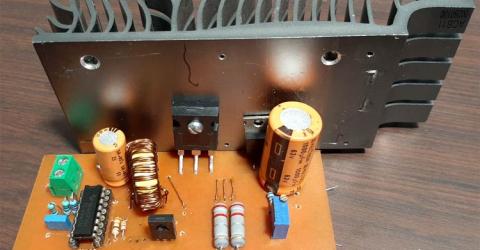
Designing a High Power, High Efficiency Boost Converter using TL494 In this article, we are going to design a TL494 Boost converter, and calculate and test a high-efficiency boost converter circuit based on the popular TL494 IC, which has a minimum supply voltage of 7V and a maximum of 40V, and as we are using the IRFP250 MOSFET as a switch, this circuit can handle a maximum current of 19Amps, theoretically (Limited by Inductor… |