

It is fair to consider a PCB itself as a component in which multiple traces are connected. Each trace is different, some are high speed, some are low speed, some are noisy, some are used by the return path of circuit current, etc. Now, as we all know, there are lots of variations in ideal circuits and real circuits. Suppose a high-frequency trace is routed with a 7mm copper trace with a 0.5mm track width, it will add Inductance, Capacitance, and resistance on the track. This makes a difficult situation for high-frequency signal lines as that capacitance and inductance could change the frequency of the signal and the ending point of the trace will produce completely different results than the starting point of the trace. The major degradation of this type of signal is due to the Impedance in PCB trace. In this article, we will understand more about PCB impedance matching, and why it is important.
What is Impedance?
You can think of Impedance as resistance in AC. Impedance is also measured in Ohms, just like Resistance, but it is very different from resistance. Resistance Ohms works in DC characteristics, but the impedance is used in AC, specifically, that has a frequency.
To ensure that the signal trace is carefully designed and the quality of the signal does not degrade over the traces, impedance needs to be controlled carefully as the impedance of the traces of a PCB is generally uncontrolled.
Importance of Impedance Matching in PCB Design
Essentially, impedance control in PCB design refers to the matching of substrate material properties with trace dimensions and locations to ensure the impedance of a trace’s signal is within a certain percentage of a specific value. Controlled impedance boards provide repeatable high-frequency performance.
Following are the reasons to control impedance in PCB design.
- At high-frequency, the signal traced on a PCB is not just a connection but acts like a component. Even a single trace has different characteristics at different points.
- Whenever the signal moves further in the traces, different impedance produces signal reflection that is dependent on the difference between two unmatched impedances. The larger impedance mismatch produces larger reflection and affects the signal integrity.
- The reflection of the signal superimposes the actual or primary signal that is often misunderstood by the high-frequency ADC, high-speed processing circuits, and fails to decode the actual signal.
Standard Impedance Values for PCB Design
Different signal traces require different impedance characteristics over the entire signal traces. Depending on the types of signal and the speed of the data transfer or frequency, the list below will give a widely accepted controlled impedance for different PCB signal traces.
It is important to remember that the Impedance needs to be maintained all over the signal path.
|
Signal Standard |
Targeted Impedance (Ohms) |
Accepted Tolerances |
|
USB |
90 |
+/- 15% |
|
HDMI |
95 |
+/- 15% |
|
IEEE 1394 |
108 |
+/- 2% |
|
Displayport |
100 |
+/- 20% |
|
VGA |
75 |
+/- 5% |
|
DVI |
95 |
+/- 15% |
|
PCIe |
85 |
+/- 15% |
|
Ethernet Cat.5 |
100 |
+/- 5% |
Thus, when routing signal traces, it is important to maintain the above impedances to maintain signal integrity.
However, other than this, specific impedance requirements are always mentioned in the datasheet of the respective component. It is advisable to go through the datasheet to get information about high-frequency traces and what are the impedance requirements of the particular signal.
PCB Impedance Matching – Example
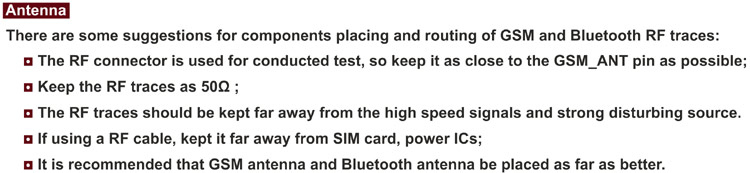
For example, let's choose a popular RF module, the SIM800 module that is widely popular in IoT due to its low cost and easy availability. Many people use this module and design a PCB which may be good for hobby projects but when this PCB will be tested for signal level integrity, the output of the SIM800 will be very poor. Not only this, in the most serious cases, the RF Antenna may provide poor results, as well as the SIM800 fails to work in the network. The major reason in almost all cases is bad PCB design, especially the RF signal Routing. The RF antenna or RF signal is a very high-frequency signal that receives data in the GSM band. This needs to be properly designed for reducing the reflection on the RF traces. The Datasheet says that the target impedance of the RF Trace should be 50 Ohms as a controlled impedance.
PCB Impedance Measurement and Calculation
Most of the signals that are just single signal paths have single-ended impedance and signals that use differential pair impedance as well as single-ended impedance.
The impedance traces depends on the following things:
- Width and Thickness of the Copper traces (In all layers)
- The dielectric constant of the core and prepreg materials
- Distance from other coppers
- The thickness of the core or prepreg material.
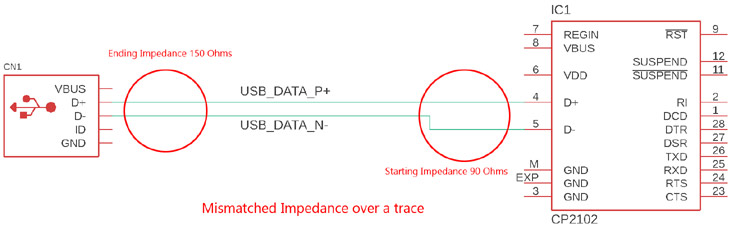
So, the above information is required for the impedance matching of signal traces. In a previous article, we have seen how to route a differential pair signal. Let's match the impedance of the same signal since differential pair routing is completed when the impedance is matched properly.
To calculate the impedance, I use Saturn PCB impedance calculator software, Inc - PCB Toolkit V8.05 that is free software and very famous among designers. It is useful to get the approximate value of the required impedance spacing, etc.
So, Impedance needs to be matched on the D+ and D- lines of the USB. Since it is a USB signal, the requirement of the impedance is 90 Ohms.
Following are my parameters-
- PCB - FR4 with a Dielectric constant of 4.6 Er
- Base copper and plating thickness both are 35um
- Conductor Height was chosen as 0.254mm
- The differential pairs will be routed either in the top layer or in the bottom layer
Let's calculate the trace thickness and trace spacing-
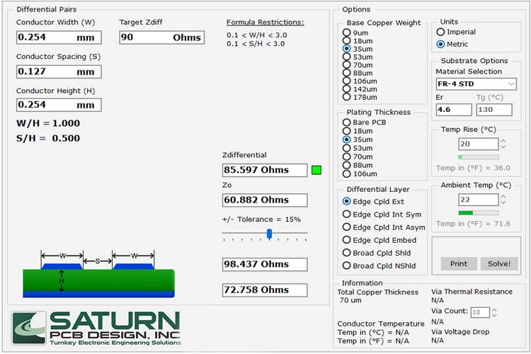
Som with a 15% tolerance and 90 Ohms targeted impedance, the conductor width required 0.254mm, spacing between both is required 0.127mm.
So, if we route the differential pair in an FR-4 board with 35um copper and plating thickness the targeted impedance will be close to 90 Ohms. It needs to be routed carefully that anywhere the spacing between the two conductors should not increase or decrease than 0.127mm and the Track width should not increase or decrease than the 0.254mm.
However, the perfect impedance value and matching after routing the trace can only be done by the manufacturer. The manufacturer needs to be updated that the board requires impedance control, and the targeted impedance is 90 Ohms in differential pair and 60 Ohms on single-ended impedance. The manufacturer of the PCB will make the PCB with the targeted impedance.
