

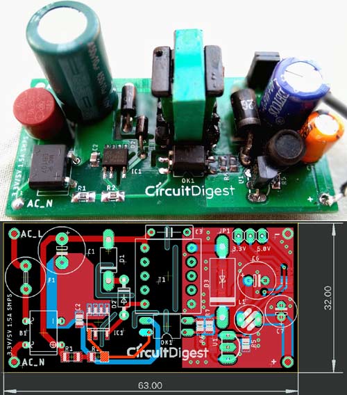
Switching power supply is a widely used power supply topology in power electronics. Whether it can be a complicated CNC Machine or a compact electronic device, as long as the device is connected to some sort of power supply an SMPS circuit is always mandatory. Improper or faulty Power supply unit could lead to a big failure of the product irrespective of how well-designed and functional the circuit may be. We have already designed quite a few SMPS Power Supply circuits like the 12V 1A SMPS and the 5V 2A SMPS using the Power Integration and Viper controller IC respectively.
Every Switching power supply uses a switch like a MOSFET or a power transistor that constantly gets turned ON or OFF depending on the switching driver specification. The switching frequency of this ON and OFF state ranges from a few hundred kilohertz to megahertz range. In such a high-frequency switching module, the PCB design tactics are far more essential and it is sometimes overlooked by the designer. For example, a poor PCB design could lead to failure of the entire circuit as well as well-designed PCB could solve many unpleasant events.
As a general rule of thumb, this tutorial will provide some detailed aspects of important PCB design layout guidelines that are essential for any kind of switch-mode power supply based PCB design. You can also check out the Design Techniques for EMI Reduction in SMPS Circuits.
First thing first, for designing a switch-mode power supply, one needs to have a clear indication of the circuitry requirement and specifications. The power supply has four important portions.
- Input and output filters.
- Driver circuitry and associated components for the driver especially control circuit.
- Switching inductors or Transformers
- Output Bridge and the associated filters.
In a PCB design, these all segments need to be separated in PCB and require special attention. We will discuss each segment in detail in this article.
Guidelines for Input and Associated filters
The input and the filter section is where the noisy or unregulated supply lines get connected into the circuit. Therefore, the input filter capacitors need to be situated in an evenly spaced distance from the input connector and the driver circuit. It is essential to always use a short length of connection for connecting the Input section with the driver circuit.

The highlighted sections in the above image are representing the close placement of the filter capacitors.
Guidelines for Driver Circuitry and Control Circuit
The driver mainly consists of an internal MOSFET or sometimes the switching MOSFET is externally connected. The switching line always gets turned ON and turned OFF in very high frequency and creates a very noisy supply line. This portion always needs to be separate from all other connections.
For example, the high voltage DC line that is directly going to the transformer (For flyback SMPS) or the DC line that directly goes to the power inductor (Buck or Boost topology-based switching regulators) should be separated.
In the below image, the highlighted signal is the high voltage DC line. The signal is routed in such a way that it is separated from other signals.

One of the noisiest lines in a switch-mode power supply design is the drain pin of the driver, whether it is an AC to DC flyback design or it can be a buck, boost or buck-boost topology-based low power switching power supply design. It always needs to be separated from all other connections as well as needs to be very short because this type of routings generally carries very high-frequency signals. The best way to isolate this signal line from others is to use PCB cutout by using milling or dimension layers.
In the below image, an isolated Drain pin connection is shown that has a safe distance from the Opto-coupler as well as the PCB cut out will remove any interference from other routings or signals.
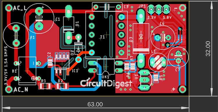
Another important point is, a driver circuit almost always has feedback or sensed line (some times more than one such as input voltage sense line, output sense line) that is very sensitive and the driver operation is entirely dependent by sensing the feedback. Any kind of feedback or sense line should be shorter in length to avoid noise coupling. These types of lines always need to be separated from the Power, switching or any other noisy lines.
The below image is showing a separate Feedback line from optocoupler to the driver.

Not only this, but a driver circuit can also have multiple types of components such as capacitors, RC filters that are required to control the driver circuit operations. Those components need to be placed closely across the driver.
Guidelines for Switching Inductors and Transformers
Switching Inductor is the largest available component in any power supply board after bulky capacitors. One bad design is to route any kind of connection between the Inductor leads. It is essential not to route any signals between the powers or filter inductor pads.

Also, Whenever Transformers are used in a power supply, especially in AC-DC SMPS, the main use of this transformer is to isolate the input with the output. Adequate distance between primary and secondary pads are required. One best way to increase creepage is by applying a PCB cutoff using a milling layer. Never use any kind of routing between the transformer leads.

Guidelines for Output Bridge and Filter Section
The output bridge is a high current Schottky diode that dissipates heat depending on the load current. In a few cases, PCB heat sinks are required that need to be created in the PCB itself by using the copper plane. The heat sink efficiency is proportional to the PCB copper area and thickness.
There are two types of copper thickness commonly available in PCBs, 35 microns and 70 microns. The higher the thickness is, the better thermal connectivity and PCB heat sink area get shortened. If the PCB is a double layer and the heated space is somewhat not available in a PCB, one can use both sides of the copper plane and could connect those two sides using common vias.
The below image is an example of PCB heatsink of a Schottky diode that is created in the bottom layer.

The filter capacitor right after the Schottky diode needs to be placed very closely across the transformer or the switching inductor in such a way that the supply loop through the Inductor, Bridge diode and capacitor gets very short. In such a way, the output ripple can be reduced.

The above image is an example of a short loop from the transformer output to the bridge diode and filter capacitor.
Reducing Ground bounce for SMPS PCB Layouts
Firstly, the ground filling is essential and separating different ground planes in a power supply circuit is another most important thing.
From the circuitry perspective, a switching power supply can have a single common ground for all components but it is not the case during the PCB design phase. As per the PCB design perspective, the ground is separated into two parts. The first portion is power ground and the second portion is analog or control ground. These two grounds have the same connection but there is a big difference. Analog or control ground is used by the components that are associated with the driver circuit. Those components use a ground plane that creates a low current return path, on the other hand, the power ground carries the high current return path. Power components are noisy and could lead to uncertain ground bounce issues in control circuitry if they are directly connected in the same ground. The below image shows how the analog and control circuitry is completely isolated from other power lines of the PCB in a single layer PCB.

These two portions need to be separated and should be connected in a particular region.
This is easy if the PCB is a double layer, like the top layer can be used as a control ground and all control circuitry should be connected in the common ground plane in the top layer. On the other hand, the bottom layer can be used as a power ground and all noisy components should use this ground plane. But those two grounds are the same connection and connected in the schematic. Now, for connecting the top and bottom layers, vias can be used for connecting both ground planes in a single place. For example, see the below image –

The above portion of the driver has all power filter related capacitors that are using a ground plane separately called Power GND, but the below portion of the driver IC is all control related components, using a separate control GND. Both grounds are the same connection but separately created. Both GND connection then joined across the Driver IC.
Follow the IPC Standards
Follow the PCB guidelines and rules as per the IPC PCB design standard. This always minimizes the error chances if the designer follows the PCB design standard described in IPC2152 and IPC-2221B. Mainly remember that the width of the traces is directly affecting the temperature and current carrying capacity. Therefore, the wrong width of the traces could lead to a temperature increase and poor current flow.
The spacing between two traces is also important to avoid uncertain failure or cross-talk, sometimes crossfires in high current high voltage application. IPC-9592B describes the recommended spacing between the power lines in Power Supply based PCB design.
Kelvin Connection for Sense Line
Kelvin connection is another important parameter in the Power Supply Board Design, because of the accuracy of the measurement which affects the ability of the control circuit. A power supply control circuit always requires some kind of measurements, be it current sensing or voltage sensing in the feedback or sense line. This sensing should be done from the component leads in such a way that other signals or traces do not interfere with the sense line. Kelvin connection helps in achieving the same, if the sense line is a differential pair, the length needs to be the same for both the traces and the trace should connect across the component leads.
For example, the Kelvin connection is properly described in the PCB design guidelines of Power controllers by Texas instruments.

The above image is showing proper current sensing using a Kelvin connection. The right connection is the proper kelvin connection that will be essential for sense line design. The PCB layout is also given properly in that document.

The PCB layout shows a close connection between the 10nF and 1nF ceramic capacitor across the driver or controller IC. The Sense line is also reflecting the proper kelvin connection. The Inner power layer is a separated source line that is connected with the same but separated source lines using multiple vias for reducing noise coupling.
