

Every Electronic device or product requires a reliable power supply unit (PSU) to operate it. Almost all devices in our home, like TV, Printer, Music Player etc. consists of a power supply unit built into it which converts the AC mains voltage to a suitable level of DC voltage for them to operate. The most commonly used of type of power supply circuit is the SMPS (Switching Mode Power Supply), you can easily find this type of circuits in your 12V adapter or Mobile/Laptop charger. In this tutorial we will learn how to build a 12v SMPS circuit that would convert AC mains power to 12V DC with a maximum current rating of 1.25A. This circuit can be used to power small loads or even be adapted into a charger to charge you lead-acid and lithium batteries. If this 12v 15watt power supply circuit doesn’t match your requirement, you can check various power supply circuit with different ratings.
12v SMPS Circuit – Design Considerations
Before proceeding with any kind of power supply design, requirement analysis has to be done based on the environment in which our Power supply will be used. Different kinds of power supply work in different environments and with specific input-output boundaries.
Input Specification
Let's start with the input. An input supply voltage is the first thing which will be used by the SMPS and will be transformed into a useful value to feed the load. As this design is specified for AC-DC conversion, the input will be Alternating current (AC). For India, the input AC is available in 220-230 volt, for the USA it is rated for 110 volts. There are also other nations which use different voltage levels. Generally, SMPS works with universal input voltage range. This means the input voltage can differ from the 85V AC to 265V AC. SMPS can be used in any country and could provide a stable output of full load if the voltage is between 85-265V AC. The SMPS should also function normally under 50Hz and 60Hz frequency as well. This is the reason why we are able to use our phone and laptop chargers in any country.
Output Specification
On the output side, few loads are resistive, few are inductive. Depending on the load the construction of an SMPS can be different. For this SMPS the load is assumed as a resistive load. However, there is nothing like a resistive load, each load consists of at-least some amount of inductance and capacitance; here it is assumed that the inductance and capacitance of the load are negligible.
The output specification of an SMPS is highly dependable on the Load, like how much voltage and current will be required by load under all operating conditions. For this project, the SMPS could provide 15W output. It is 12V and 1.25A. The targeted output ripple is selected as less the 30mV pk-pk at 20000 Hz bandwidth.
Based on the output load, we also have to decide between the designing a Constant Voltage SMPS or Constant Current SMPS. Constant voltage means the voltage across the load will be constant and the current will be changed accordingly with the changes in load resistance. On the other hand, constant current mode will allow the current to be constant but change the voltage accordingly with the changes in load resistance. Also, both CV and CC can be available in an SMPS but they cannot work in a single time. When both options exist in an SMPS, there needs to be a range when the SMPS will change its output operation from CV to CC and vice versa. Normally CC and CV mode chargers are used to charge lead acid or lithium batteries.
Input and Output Protection Features
There are various protection circuits that can be employed on the SMPS for safer and reliable operations. The protection circuit protects the SMPS as well as the connected load. Depending on the location, the protection circuit can be connected across input or across the output. The most common input protection is Surge Protection and EMI filters. Surge protection protects the SMPS from input surges or AC overvoltage. EMI filter protects the SMPS from EMI generation across the input line. In this project, both features will be available. Output protection includes short circuit protection, over-voltage protection and over current protection. This SMPS design will also include all of these protection circuits.
Selection of the Power Management IC
Every SMPS circuit requires a Power Management IC also known as switching IC or SMPS IC or Drier IC. Let’s sum up the design considerations to select the ideal Power Management IC that will be suitable for our design. Our Design requirements are
- 15W output. 12V 1.25A with less than 30mV pk-pk ripple at full load.
- Universal input rating.
- Input surge protection.
- Output short circuit, over voltage and over current protection.
- Constant voltage operations.
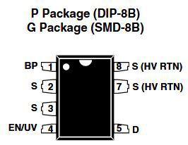
From the above requirements there is wide range of ICs to select from, but for this project we have selected Power integration. Power integration is a semi-conductor company that has a wide range of power driver ICs in various power output ranges. Based on the requirements and availability we have decided to use the TNY268PN from tiny switch II families.
In the above image, the maximum power 15W is shown. However, we will make the SMPS in the open frame and for the universal input rating. In such a segment, TNY268PN could provide 15W output. Let’s see the pin diagram.
Designing the 12v 1Amp SMPS Circuit
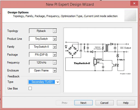
The best way to build the circuit is to use Power integration’s PI expert software. It is excellent power supply design software. The Circuit is constructed using Power Integration IC. The design procedure is explained below, alternatively you can also scroll down for the video explaining the same.
Step -1: Select the Tiny switch II and also select the desired package. We selected the DIP package. Select the Enclosure type, Adapter or Open Frame. Here Open Frame is selected.
Then select the Feedback type. It is essential as Flyback topology is used. TL431 is an excellent choice for feedback. TL431 is a shunt regulator and it will provide excellent over-voltage protection and accurate output voltage.
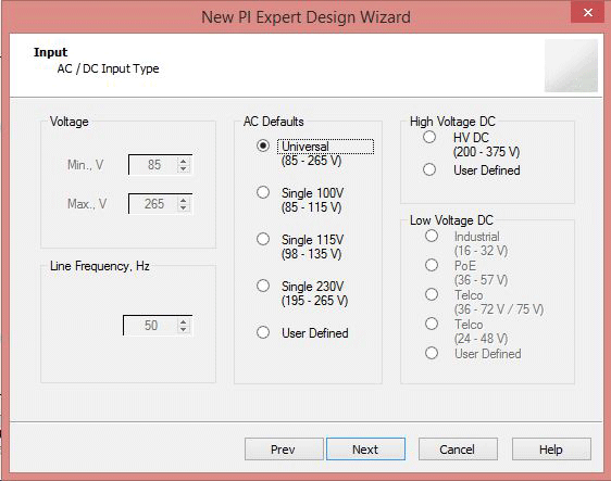
Step-2: Select the input voltage range. As it will be a universal input SMPS, the input voltage is selected as 85-265V AC. Line Frequency is 50 Hz.
Step- 3:
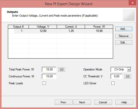
Select the output voltage, current, and wattage. The SMPS rating will be 12V 1.25A. The wattage is showing 15W. The operation mode is also selected as CV, means constant voltage operation mode. Finally, everything is done in three easy steps, and the schematic is generated.
12V SMPS Circuit Diagram and Explanation
The below circuit is slightly modified to suit our project.

Before going straight into building the prototype part, let’s explore the 12v SMPS circuit diagram and its operation. The circuit has the following sections
- Input surge and SMPS fault protection
- AC-DC conversion
- PI filter
- Driver circuitry or Switching circuit
- Under-voltage lockout protection.
- Clamp circuit
- Magnetics and galvanic isolation
- EMI filter
- Secondary Rectifier and snubber circuit
- Filter Section
- Feedback section.
Input surge and SMPS fault protection
This section consists of two components, F1 and RV1. F1 is a 1A 250VAC slow blow fuse and RV1 is a 7mm 275V MOV (Metal Oxide Varistor). During a high voltage surge (more than 275VAC), the MOV became dead short and blows the input Fuse. However, due to the slow blow feature, the fuse withstands inrush current through the SMPS.
AC-DC conversion
This section is governed by the diode bridge. These four diodes (inside DB107) make a full bridge rectifier. The diodes are 1N4006, but standard 1N4007 can do the job perfectly. In this project, these four diodes are replaced with a full bridge rectifier DB107.
PI filter
Different states have different EMI rejection standard. This design confirms EN61000-Class 3 standard and the PI filter is designed in such a way to reduce the common-mode EMI rejection. This section is created using C1, C2, and L1. C1 and C2 are 400V 18uF capacitors. It is an odd value so 22uF 400V is selected for this application. The L1 is a common mode choke that takes differential EMI signal to cancel both.
Driver circuitry or switching circuit
It is the heart of an SMPS. The transformer's primary side is controlled by the switching circuit TNY268PN. The switching frequency is 120-132khz. Due to this high switching frequency, smaller transformers can be used. The switching circuit has two components, U1, and the C3. U1 is the main driver IC TNY268PN. The C3 is the bypass capacitor which is needed for the working of our driver IC.
Under-voltage lockout protection
Under-voltage lockout protection is done by the sense resistor R1 and R2. It is used when the SMPS goes into the auto-restart mode and sense the line voltage.
Clamp circuit
D1 and D2 are the clamp circuit. D1 is the TVS diode and D2 is an ultra-fast recovery diode. The transformer acts a huge inductor across the power driver IC TNY268PN. Therefore during the switching off-cycle, the transformer creates high voltage spikes due to the leakage inductance of the transformer. These high-frequency voltage spikes are suppressed by the diode clamp across the transformer. UF4007 is selected due to the ultra-fast recovery and P6KE200A is selected for the TVS operation.
Magnetics and galvanic isolation
The transformer is a ferromagnetic transformer and it not only converts the high voltage AC to a low voltage ac but also provide galvanic isolation.
EMI filter
EMI filtering is done by the C4 capacitor. It increases the immunity of the circuit to reduce the high EMI interference.
Secondary Rectifier and Snubber circuit
The output from the transformer is rectified and converted to DC using D6, a Schottky rectifier diode. The snubber circuit across the D6 provides suppression of the voltage transient during switching operations. The snubber circuit consist one resistor and one capacitor, R3, and C5.
Filter Section
The filter section consists of a filter capacitor C6. It is a Low ESR capacitor for better ripple rejection. Also, an LC filter using L2 and C7 provide better ripple rejection across the output.
Feedback section
The output voltage is sensed by the U3 TL431 and R6 and R7. After sensing the line, U2, the optocoupler is controlled and galvanically isolating the secondary feedback sensing portion with the primary side controller. The Optocoupler has a transistor and a LED inside of it. By controlling the LED, the transistor is controlled. Since the communication is done by optically, it has no direct electrical connection, therefore satisfying the galvanic isolation on the feedback circuit too.
Now, as the LED directly controls the transistor, by providing sufficient bias across the optocoupler LED, one can control the optocoupler transistor, more specifically driver circuit. This control system is employed by the TL431.As the shunt regulator has a resistor divider across its reference pin, it can control the optocoupler led which is connected across it. The feedback pin has a reference voltage of 2.5V. Therefore, the TL431 can be active only if the voltage across the divider is sufficient. In our case, the voltage divider set to a value of 12V. Therefore, when the output reaches 12V the TL431 gets 2.5V across the reference pin and thus activate the optocoupler's LED which controls the transistor of the optocoupler and indirectly controls the TNY268PN. If the voltage is not sufficient across the output the switching cycle is immediately suspended.
First, the TNY268PN activates the first cycle of switching and then sense it's EN pin. If everything is alright, it will continue the switching, if not, it will try once again after sometimes. This loop gets continued until everything gets normal, thus preventing shortcircuit or overvoltage issues. This is why it is called flyback topology, as the output voltage is flown back to the driver for sensing related operations. Also, the trying loop is called a hiccup mode of operation on the failure condition.
The D3 is a Schottky barrier diode. This diode converts the high frequency AC output to a DC. 3A 60V Schottky Diode is selected for reliable operation. R4 and R5 is selected and calculated by the PI Expert. It creates a voltage divider and passes the current to the Optocoupler LED from the TL431.
R6 and R7 is a simple voltage divider calculated by the formula TL431 REF voltage = (Vout x R7) / R6 + R7. The reference voltage is 2.5V and the Vout is 12V. By selecting the value of R6 23.7k, the R7 became 9.09k approximately.
Fabricating PCB for 12v 1A SMPS Circuit
Now that we understand how the schematics work, we can proceed with building the PCB for our SMPS. Since this is an SMPS circuit a PCB is recommended as it could deal with noise and isolation problem. The PCB layout for the above circuit is also available for download as Gerber from the link
Now, that our Design is ready it is time to get them fabricated using the Gerber file. To get the PCB done is quite easy, simply follow the steps below
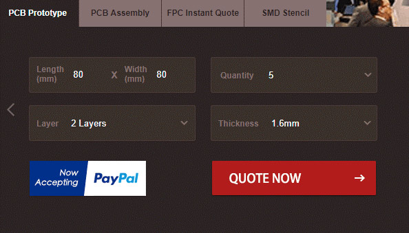
Step 1: Get into www.pcbgogo.com, sign up if this is your first time. Then, in the PCB Prototype tab enter the dimensions of your PCB, the number of layers and the number of PCB you require. Assuming the PCB is 80cm×80cm you can set the dimensions as shown below.
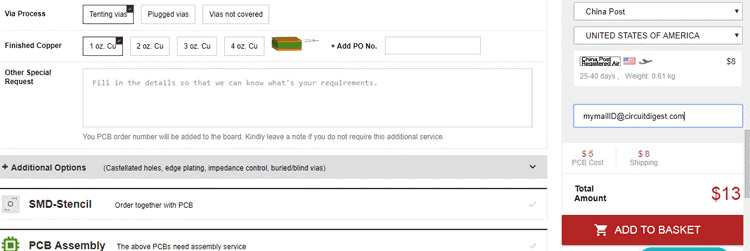
Step 2: Proceed by clicking on the Quote Now button. You will be taken to a page where to set few additional parameters if required like the material used track spacing etc. But mostly the default values will work fine. The only thing that we have to consider here is the price and time. As you can see the Build Time is only 2-3 days and it just costs only $5 for our PSB. You can then select a preferred shipping method based on your requirement.
Step 3: The final step is to upload the Gerber file and proceed with the payment. To make sure the process is smooth PCBGOGO verifies if your Gerber file is valid before proceeding with the payment. This way you can sure that your PCB is fabrication friendly and will reach you as committed.
Assembling the PCB
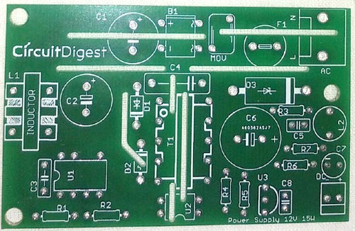
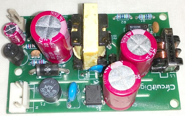
After the board was ordered, it reached me after some days though courier in a neatly labeled well packed box and like always the quality of the PCB was awesome. The PCB that were received by me is shown below
I turned on my soldering rod and started assembling the Board. Since the Footprints, pads, vias and silkscreen are perfectly of the right shape and size I had no problem assembling the board. My PCB clamped to the soldering vice is shown below.
Components Procurement
All components for this 12v 15w SMPS circuit are procured as per the schematic. The detail BOM can be found in the below excel file for download.
Almost all components are readily available to be used off the shelf. You might find trouble finding the right transformer for this project. Normally for an SMPS circuit switching flyback transformer is not available from the vendors directly, in most cases you have to wind your own transformer if you need efficient results. However it is also okay to use a similar flyback transformer and your circuit will still work. The ideal specification for our transformer will be provided by the PI Expert software that we used earlier.
The Mechanical and Electrical diagram of the transformer obtained from PI Expert is shown below.
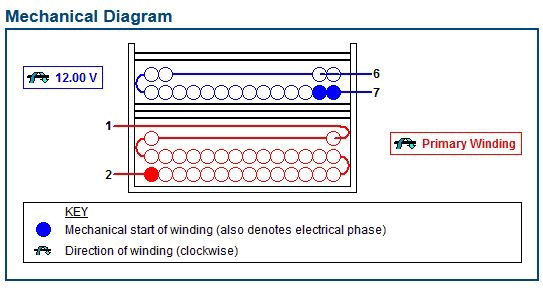
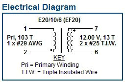
If you are not able to find the right vendor, you can salvage a transformer from a 12V adapter or other SMPS circuits. Alternatively you can also build your own transformer buy using the following materials and winding instruction.
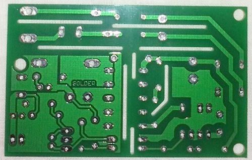
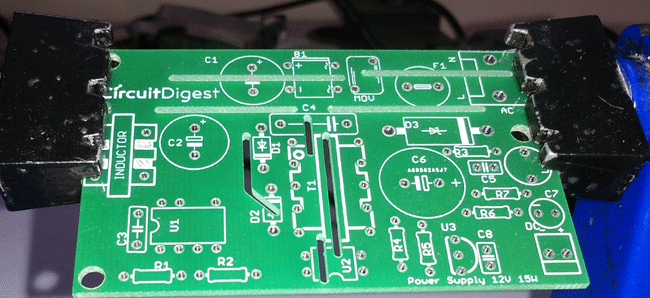
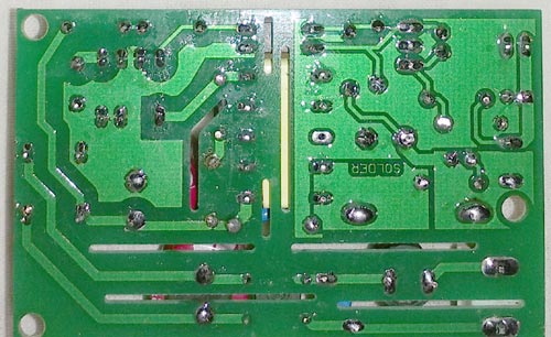
Once all the components are procured, assembling them should be easy. You can use the Gerber file and BOM for reference and assembled the PCB board. Once done my PCB front side and back side looks something like this below
Testing our 15W SMPS circuit
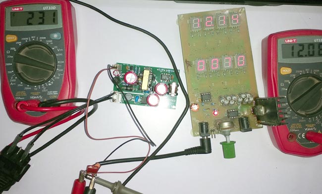
Now that our circuit is ready, it’s time to take it for a spin. We will connect the board to our Ac mains through a VARIAC and load the output side with a load machine and measure the ripple voltage to check the performance of our circuit. Full testing procedure video can also be found at the end of this page. The below image shows the circuit tested with an input AC voltage of 230V AC for which we get an output of 12.08V
Measuring Ripple Voltage using Oscilloscope
To measure the ripple voltage with oscilloscope, change the input of scope to AC with a gain of 1x. Then connect a low-value Electrolytic capacitor and a low-value ceramic capacitor for picking up noise reductions due to wirings. You can refer to page 40 of this RDR-295 document from Power Integration for more information on this procedure.
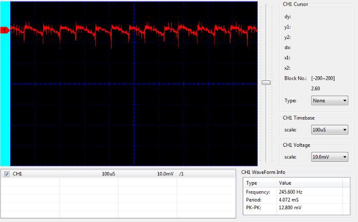
The below snapshot was taken at no-load condition on both 85VAC and 230VAC. The scale is set at 10mV per division and as you can see the ripple is almost 10mV pk-pk.
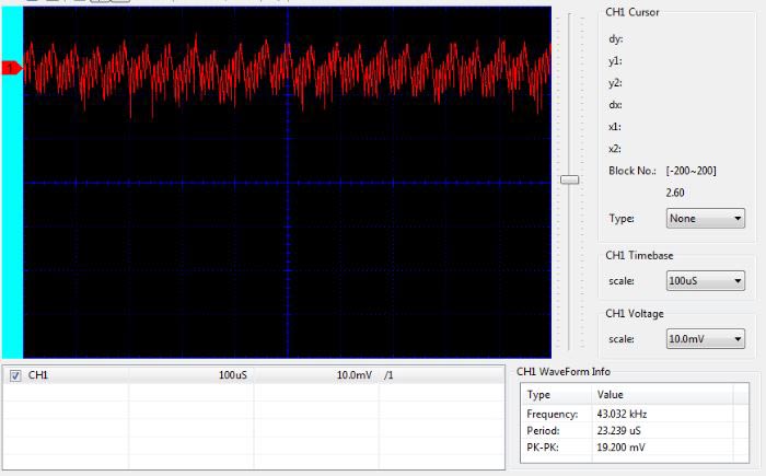
At 90VAC input and with a full load, the ripple can be seen at around 20mV pk-pk
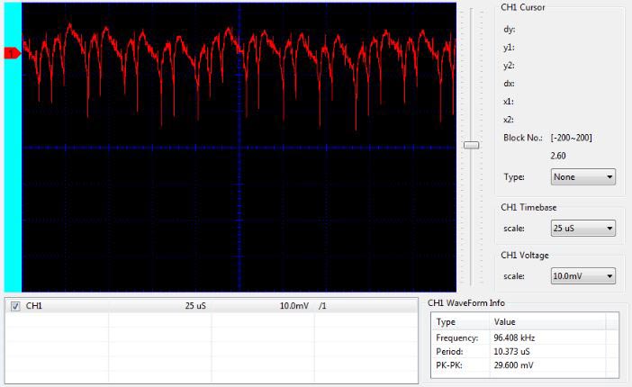
In 230VAC and on the full load ripple voltage is measured at around 30mV pk-pk which is the worst case scenario
That is it; this is how you can design your own 12v SMPS circuit. Once you have understood the working, you can alter the 12v SMPS circuit diagram to suit for your voltage and power requirements. Hope you understood the tutorial and enjoyed learning something useful. If you have any questions leave them in the comment section or use our forums for technical discussions. Will meet you again with another interesting SMPS design, until then signing off….
Comments
Hello Vijay,
Thank you for the good work. My question is, can i use this power supply to charge 12V 7AH Lead acid battery?
This IC is available in the local market that's why it is selected for my application as an SMPS design tutorial for the hobbyist.
However,
If you are looking for SMPS production then choose the latest design.
You can make the same design along with pi expert 10.1 by selecting the same parameters on TNY switch III or IV. The ICs are available on element14.com or in mouser.in
The design is made using PI Expert 8.6.
I did not understand your other questions. Kindly provide more info.
Hi, I have to thank you for sharing this excellent job and detailed tutorial. I tried to use your gerber files on PCBgogo, PCBcart and JLCPCB, without success. It does not open correctly or does not open.
Anyway, it's a beautiful work and it helped me a lot to understand the subject. Thanks! Cheers!
I noticed that the design of the transformer does not include an auxiliary winding only the primary and the secondary. I am sure there is a logical explanation for this (that I am not aware of, my knowledge of electronics is limited, I am a hobbyist). Could you please explain this to me?
Hi,
A query:
12V X 9.09 / (9.09 + 23.7) = 3.3V and not 2.5V...any reason? Is there a diode drop somewhere?
Many thanks for publishing this.
hi could anyone tell me alternative or availability of these components.i am trying to fix my power supply, transistors- h945 p 8b3
STTH1002CT GKDSNVU HIGH EFFICIENCY ULTRAFAST DIODE
STPS2045CT 75ACDVW SCOTTY - 2 of them.
thanks
Dear Sir,
I am trying to design this project, but 6mH, 1.6A (common mode choke) is not available in market can you please suggest me some alternative for that component.
sir can you give more specifications about transformer like inductance

This product is not recommended for new designs. it on
https://www.power.com/sites/default/files/product-docs/tny263_268.pdf
https://prnt.sc/p13w31
It just published by you on 2 Sept 2019
I have doubt some circuit design i wrote on your youtube
Thanks, Lot for Nice Video Beciase so many days I was looking SMPS design Thanks, Lot for Nice Video