

There are multiple instances where a well-designed circuit has failed in the POC stage or in the Production Stage because of a bad PCB design. PCB design is an art where all components sit together and the connections are done via copper traces.
It may seem to be an easy job to connect all but is rather a difficult task as different things of the circuit make different outputs in the real field. It is very difficult to summarize the issues that cause the failure of the circuit, but one common reason is the PCB ground bounce issue where the ground return path of the circuit does not have a proper copper area and causes resistance in the circuit. This makes it very difficult to handle the op-amps in such cases as they are very sensitive in terms of measurement (If used as a sense amplifier) or for the RF circuits that tend to have EMI interference in high-frequency operations. One common failure is not having ground stitching in the design and thus affecting the poor ground bounce.
Previously, we have discussed different types of vias in PCB that you can use in a PCB design. If you are interested in more PCB design guide articles, you can also check out the article on PCB Power Supply Design Guidelines.
What is Via Stitching?
Before understanding what is stitching via, let's understand what is the Via. Take a look at the image below.
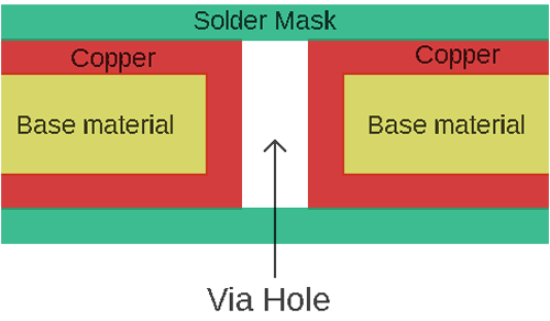
The above image shows a two-layer board that has a base material. This base material can be a wooden-clad board or glass board type of material. This material or specifically this board has copper above and below the plane. Thus, the thing looks like this.
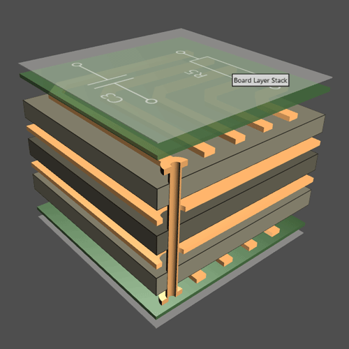
The above image is showing different layers in the multi-stack board. Now, if someone wants to make a connection from the above copper plane to the below copper plane, he/she will have to add a VIA. VIA is nothing but a hole drilled through the base material of PCB during the production stage of the PCB, the inner layer of this hole is filled with copper to allow it to carry the copper traces across different layers of the PCB.
Now, since this can be made in any place, why not use it in the actual Larger Copper plane of the PCB? Well, yes it can be done, and when you do that it is called Via Stitching
Understanding PCB Via Stitching
A via stitching is a process where multiple numbers of vias are used to drill the copper areas on different layers and then connected. It is generally done on the larger copper planes, such as Ground filling planes, Power planes, etc.
For example, there are different types of Via stitching processes available in the PCB design that are different from others but at the same time, it is the same in terms of the concept. The different Via stitching can be summarised as:
- Constant Ground Via stitching
- Thermal Via stitching
- Shielding Via stitching
Constant Ground Via Stitching
This is the most commonly used Via stitching technique used in most PCBs. Ground Planes via stitching are done to ensure shorter ground return paths in PCB from the load devices to the power source. Thus, it maintains a healthy ground return path obtaining low resistance in the ground plane. It produces lower heat dissipation since the copper pour is larger and is connected with the top and bottom layer or with the other layers as well if the design supports more than two layers of the copper plane, resulting in a low drop resistance. It keeps the balance of the copper resistance across all places in the PCB. Thus, if someone measures the voltage drop between ground planes at different places, due to different resistance, different voltage drop causes the ground bounce issue. Via stitching is very effective and it takes a low effort compared with debugging a faulty ground bounce in the PCB.
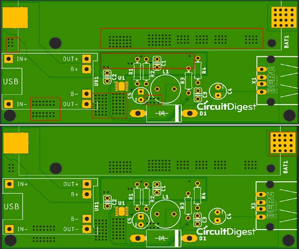
At Circuit Digest, we made multiple PCBs that are successful in the working phase using the Via stitching technique on the ground plane. Just for an example, below PCB is from the USB Powered Raspberry Pi UPS, where the Via stitching is used successfully. Here are some images with shows via stitching, I have highlighted them in red for better understanding.
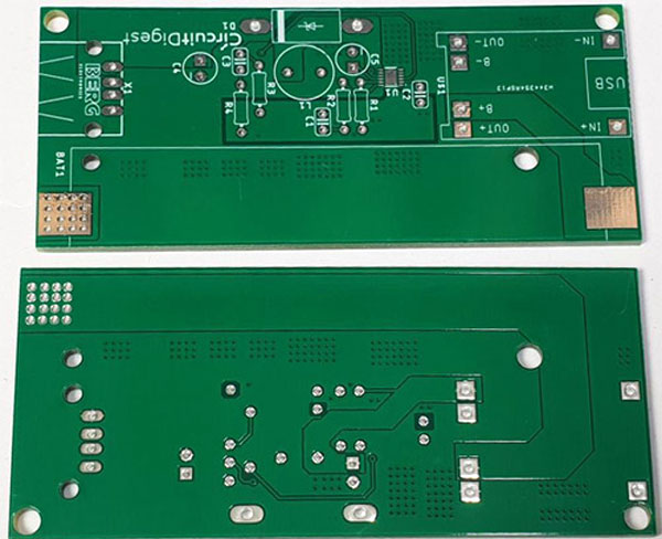
Not only in Ground Plane, it can also be used for other desired places where the Copper pour needs to be perfect. Stitching via is used in a different layer other than the Ground plane. The actual images of the PCB are shown below.
Thermal Via Stitching
PCB Based heatsink is much more useful in most instances if properly designed. A key component of the PCB-based heatsink is the Thermal Via Stitching. We have made multiple projects where thermal via stitching is used to provide excellent thermal conductivity over multiple copper planes (Top & Bottom). Let's see the below example from our MPPT Solar charger project.
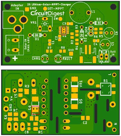
In the above PCB or others, it is very helpful in distributing the heat over the copper plane. As the PCB is much more conducive on the layer segment where the high power component is seated. It becomes too hot and the heat is only distributed sideways whereas the PCB core and the other opposite layer stays cooler than the active traces. Stitching at this point makes it more thermally conductive through-plane conductivity which further dissipates the heat to the core and further to the connected opposite plane which reduces the overall junction temperature of the targeted high power component.
Shielding Via Stitching
Via shielding is done for an EMI-related reason on high-frequency RF or Mixed-signal circuits mainly in WiFi, Bluetooth, and other wide bands of high-frequency elements that can be affected due to the EMI interference. It is also termed a PCB picket fence.
Generally, it is created using a single or multiple rows of vias stitched across the perimeter of the large copper plane that is too close to the high-frequency tracks. The design given below uses the Via shielding on a 4-layer circuit board.
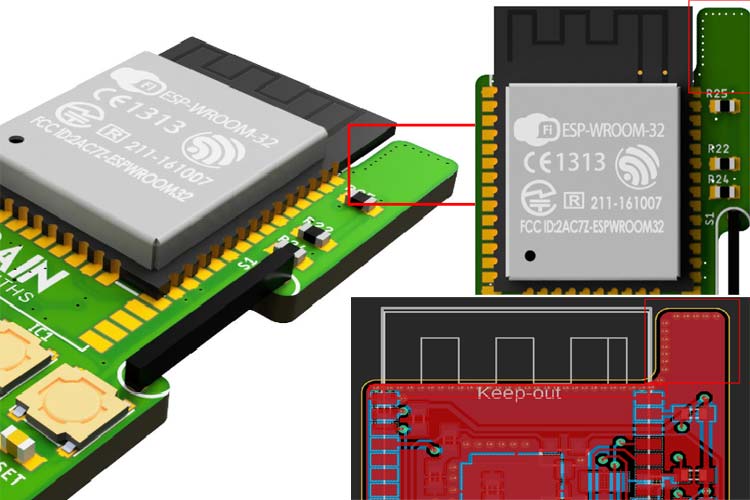
As we can see, it is done across the perimeter of the ground plane that is too close to the Antenna of the WiFi module.
Generally, it is suggested to use the Shielded Via stitching on an RF board where the vias are spaced at a minimum of 1/10th of the targeted wavelength of the highest frequency that needs to be shielded from interfacing. In some practices, it is done with 1/8th of spaces as well. But the major attention is to keep the vias spacing small compared with the wavelength in the substrate dielectric.
However, the above points are important for understanding the Via shielding. Different people have different opinions on this and this could be a major debate on what to use and where to use it. If you have any feedback on the above points or wish to add some or discuss/debate on the same, please use the Electronics forum.
