

Raspberry Pi is a small or mini-computer that can be used in different types of small to large embedded, IoT, Industrial IoT applications. As this is a computer that could run different operating systems, a shutdown of this minicomputer is an important thing to ensure that everything is saved, the operating system properly ended all required tasks, and it is safe to turn the device off. Uncertain failure of power could damage the Pi as well as the operating system could also break down. Previously we have built many Raspberry Pi Projects and most of them needed to work 24x7 so, this project can act like a Raspberry pi UPS hat and can be used to keep our raspberry pi on during power failure.
To save the Pi during uncertain power falls or unintended shutdowns, a UPS can be constructed, same as the UPS backups which are used in our home or offices. Here in this project, we will make the RPI UPS power supply that could provide sufficient time to save the code in RPi as well as this can be used as a separate power supply unit for backup also. We have built this project on PCB and have used PCBWay to fabricate the boards for this project. In the following sections of the article, we have covered in detail the complete procedure to design, order, and assemble the PCB boards for this Raspberry Pi UPS Hat from PCBWay so that you can also easily build one on your own. So let's get started.
Specifications of our Raspberry Pi UPS
The specifications for our compact RPI UPS backup are given below:
- Powered by the widely popular Lithium-Ion 18650.
- Can provide current output up to 1.5A (Continuous) and 2.5A (Peak).
- Battery charging feature from the USB cable and could use any 5V standard mobile phone charger.
- Overcharge, auto-cut off, and a deep discharge protection feature.
- Easy USB Type-A output connector.
- Compact setup that could easily fit in an enclosure box.
- Efficiency approximately more than 85%.
Since this design is done with the mind that a Raspberry Pi could work at full load, it is important to know how much current Raspberry Pi draws. As there are multiple of variants available for RPI, overall current consumption for each can be seen in the below chart :
|
Model |
Condition |
Current Draw (Max) |
|
Rpi 4 B |
400% CPU Load |
1280 mA |
|
RPi 3 B+ |
400% CPU Load |
980 mA |
|
RPi 3 B |
400% CPU Load |
730 mA |
|
RPi 2 B |
400% CPU Load |
400 mA |
|
RPi 2B with SSD |
400% CPU Load + 1x 64GB SSD USB |
1250 mA |
Thus, having 1.5A of headroom is a successive way to run RPI. But, as per the datasheet, the peak current could be 2.5A. It is important to have up to 3A of sourcing capability in the PSU device retaining 1.5A of continuous current capabilities.
Components used to design our Custom Uninterruptible Power Supply (UPS)
- Lithium Battery 18650 1200mAH
- TP4056 - Battery Charging / Protection Module (Micro USB)
- 10uF 10V capacitor
- 100k resistor
- 620R resistor 1%
- 10nF 16V capacitor
- 2.2uH barrel Inductor with at least 6A capability
- 0.1uF capacitor 16V
- SR360 Diode
- 100pF 10V capacitor
- 22uF 10V capacitor
- 2k resistor with 1% tolerance
- 6.1k resistor with 1% tolerance
- USB A connector
- 18650 Battery holder
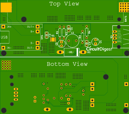
Raspberry Pi UPS Circuit Diagram
Here in the schematic, we can observe multiple resistors and capacitors, and each playing a specific role in proper functioning of the module. The C2(1uF) is the soft-start capacitor. It is used to compensate with Inrush current when high capacitive loads are connected across the output. Due to this capacitor, the switching driver will slowly turn on the switching element, which is inductor L1 (2.2uH). This L1 will be turned on and off, and during this, it will deliver power to the output Schottky diode SR360. SR360 is a 3A 60V Schottky rectifier diode that converts the high-frequency output from the Inductor L1 and to also prevents any reverse current to the circuit.
Resistors R3(6.1K ohm) and R4(2K ohm) are two feedback resistors that provide necessary feedback across the switching regulator. The divided voltage or the feedback voltage will be always 1.245 across the FB pin of the regulator. Thus, it will increase the voltage up to 5V and due to this 2k and 6.1k resistor, the feedback voltage will reach 1.245V. The C3 is used to smooth out the feedback line.
620R and 10nF, R1 and C1 are required for the stable operation of the converter.
C4 and C5 is the filter capacitor for input and output.
Schematic and the Working for the RPI UPS

Let’s have a look at the schematic and the pin diagram of the IC used in our raspberry pi battery backup module. The PI UPS module is a simple circuit and can be understood easily. For the ease of understanding, I have divided the module into two parts or stages:
- Battery charging circuit
- Switching Boost regulator.
The Battery charger:
For simplicity and without providing additional efforts, we have chosen an excellent battery charger module TP4056. It is a battery charger with all protection modules that are capable of charging a lithium-Ion battery at 1A. Additionally, it has a micro-USB port. Thus, it is very easy to solder this module onto the PCB and get the USB charging feature with all types of charging protection without adding any additional efforts of choosing the component, designing the circuit and then procuring the components and finally soldering it over the board. In most of the cases, the standard lithium-ion battery charging IC costs more than the entire cost of this module. So, this module could be used as a low-cost alternative. This module also has an additional feature of LED indicators, which provides us with the charge state of the Li-ion battery via two separate LED’s.
The Switching Boost regulator:
Lithium battery provides 3.2V to 4.2V output during no charge and full charge conditions. Typically, the battery voltage remains 3.7V-4.1V at optimum charge conditions. Thus, we need some sort of switching regulator that could provide 5.0V at the output. At the same time, we need to choose the switching regulator with the required current range also which is 3A. Here, we chose the switching regulator MIC2253, which is a 3.5A switching regulator that uses 1MHz PWM to generate the output voltage. As the switching frequency is 1MHz, this opens up the possibilities to use a smaller inductor that could deliver high power in a tiny size. To compensate for the battery voltage, it has a 2.5V to 10V input voltage range, which is ideal as per our design requirement.
Understanding the pin descriptions of MIC2253:
Before bringing any IC to use, we should learn about its pin description to get better clarity about the IC and its functions.
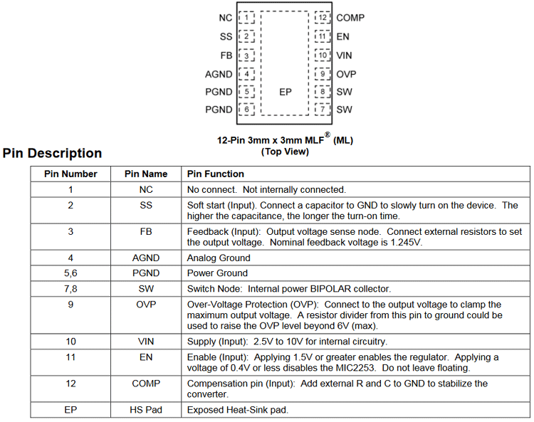
→ Please check that this chip has AGND and PGND. Both are the same in respect of schematic as both pins are Ground. But, it is a very important thing and completely different from each when it comes to the PCB design and prototyping phase. We will discuss this later in the PCB section.
PCB Design for our Raspberry Pi UPS
Here comes the complex part of this project. Why? Let’s have a look at that:
- Thermal Compensation - 3A output at 5V equivalent to a 15W on trace outrage
- Very High Frequency - 1 Mhz
- The internal construction of the MIC2253
Let's see how this can be handled. But before proceeding, if you are not careful enough, the circuit will fail. Thus, it is my advice for you to use the PCB provided on our website circuit digest.
Improper PCB design in this chip could lead to the following problems:
- Unintended shutdown due to thermal protection triggering
- High spikes induced across the output
- Very high ripple due to uncertain Ground noise
- A high ground bounce could affect the RPI.
1. Thermal Compensation - 3A output at 5V equivalent to a 15W on trace outrage:
First of all, always make high power boards in double layers where PCB heat sinks are required.
The Ground plane used is the total dissipated area where thermal conduction from the chip will happen.
Let's calculate the surface area-
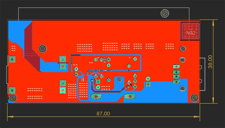
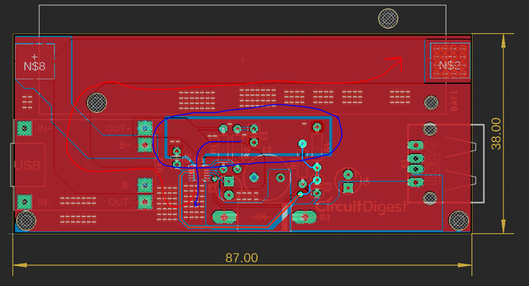
As per the design data the board is: 87mm x 38mm = 3306 sq mm.
Now the copper surface area with 100% fill will be equivalent to 3306 x 2 = 6612 sq mm.
My design shows that the total ground pour on the polygonic layer is equivalent to 69.73%. Let's assume it to be 70%.
Thus my heat sink generation on 2 dimensional view will be: 6612 x 70% = 4628 sq mm
Now, since it is copper, it has a physical thickness. There are two types of copper thickness available which are 30um and 70um. 70um is costlier. Thus, in 3D form, my copper surface will be 4628 + (4628 x 0.035) = 4789 for 35um and for 70um, it will be approximately 5000 sq mm.
It is a very poor and rough calculation since thermal conduction will not be even at all places, depending on operating and ambient temperature, atmospheric pressure, and all. But let's not dig into that part. If we roughly assume that 50% of the 5000 sq mm is doing its job, then 2500 sq mm will be our device heat sink for MIC2253, which is sufficient.
Now the traces are made thicker as per the minimum IPC standard to compensate with this:
2. Very High Frequency - 1 Mhz:
Mhz range is quite the first stage of RF design. At this stage it became difficult to isolate traces from stray capacitance and create a mini version of the RLC circuit as the traces are made of copper it has resistance and inductance, glass boards between two traces are capacitive.
Avoided FB trace to route close across the inductor or below from the inductor.
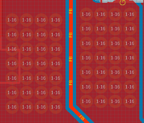
Provided ground stitching across the FB pin at the incomer in respect of the MIC2253.
3. The internal construction of the MIC2253:
The construction of the MIC2253 uses noisy and sophisticated analog circuits as well as high-power pass transistors. Now, as the current is 3.5A, during the startup, a huge load will provide a slight drop in the voltage and this leads to a problem in the sensing comparator.
See the internal construction where two separate grounds are shown but they are common ground:
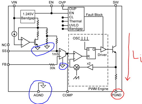
The blue one is Analog Ground which is used by all-analog circuits whereas the red one is Power GND used by all load circuits and the load current Li will pass through the pass transistor. Separating these two is essential.
The red one is the power ground whereas the blue one is the analog ground, which is completely separated from the Actual ground plane. It is not even connected in the bottom side also:
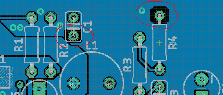
The R4 and C1 are only connected via a separate top-side ground path not even in the bottom ground polygonic plane.
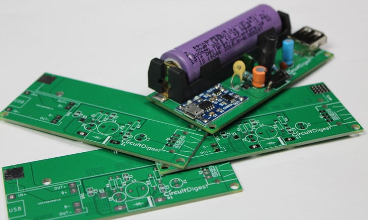
Fabricating our Raspberry Pi UPS using PCBWay.
Now that we understand how the schematics work, we can proceed with building the PCB for our project. Click on the link to check all the PCB projects we have built previously, you can also find the NodeMCU GPS Tracker PCB design file and GERBER file in the link below.
Now that our Design is ready, it is time to get them fabricated using the Gerber file. Getting your PCB fabricated from PCBWay is easy; simply follow the steps given below.
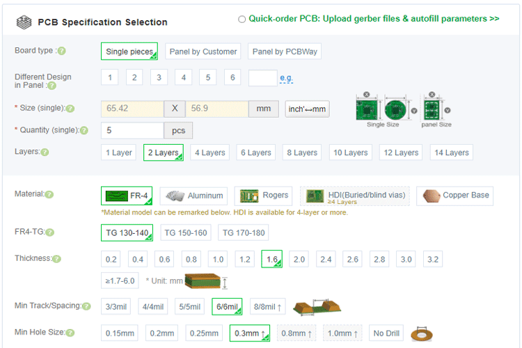
Step 1: Go to https://www.pcbway.com/, sign up if this is your first time. Then, in the PCB Prototype tab, enter the dimensions of your PCB, the number of layers, and the number of PCB you require.

Step 2: Proceed by clicking on the ‘Quote Now’ button. You will be taken to a page where to set a few additional parameters if required, like the material used track spacing, etc. but usually, the default values work fine.
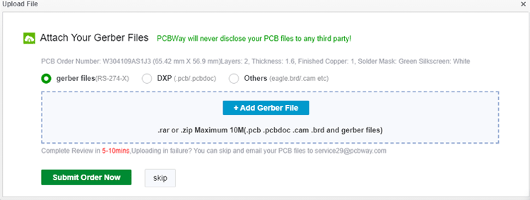
Step 3: The final step is to upload the Gerber file and proceed with the payment. To make sure the process is smooth, PCBWAY verifies if your Gerber file is valid before proceeding with the payment. This way, you can be sure that your PCB is fabrication-friendly and will reach you as committed.
Assembling our Raspberry Pi UPS Board
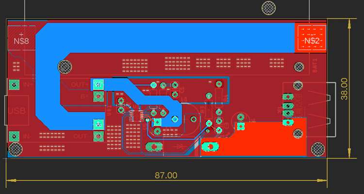
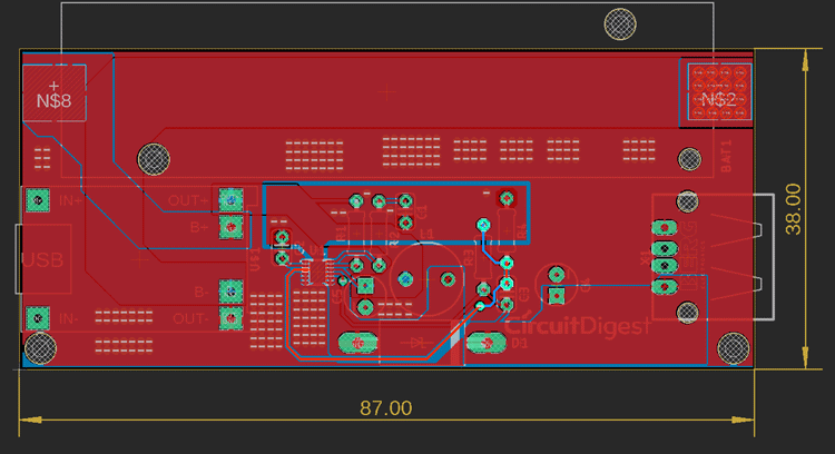
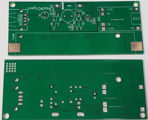
After a few days, we received our PCB from PCBWay in a neat package and as you can see below, the PCB quality was good as always. The top layer and bottom layer were seamlessly done with proper visa and track spacing.
After making sure that the tracks and footprints were correct, I proceeded with assembling the PCB. The completely soldered board looked like as shown in the image below.
Raspberry Pi UPS Board- Testing and Working
Once the board was ready, I started testing it. I powered it using a micro-USB adapter and used my multimeter to check for the output on the boost converter side.
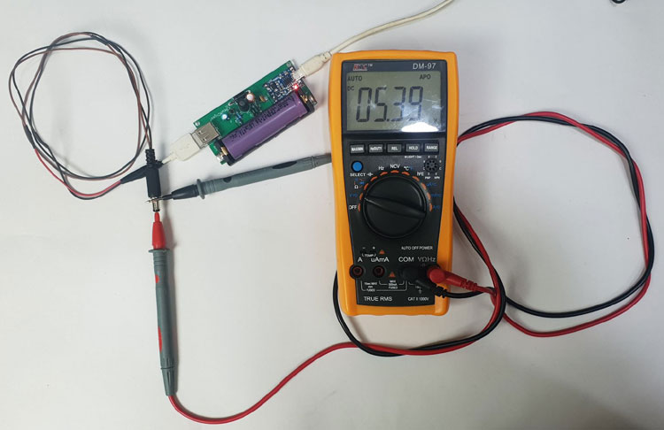
As we can observe using the multimeter that the output boosted voltage from a 3.7V Li-ion cell is 5V, which is enough to power up our Raspberry Pi module. As we have our 5V output ready, it's now time to plug in our Rpi module.
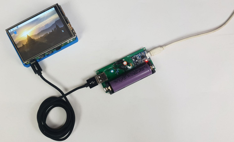
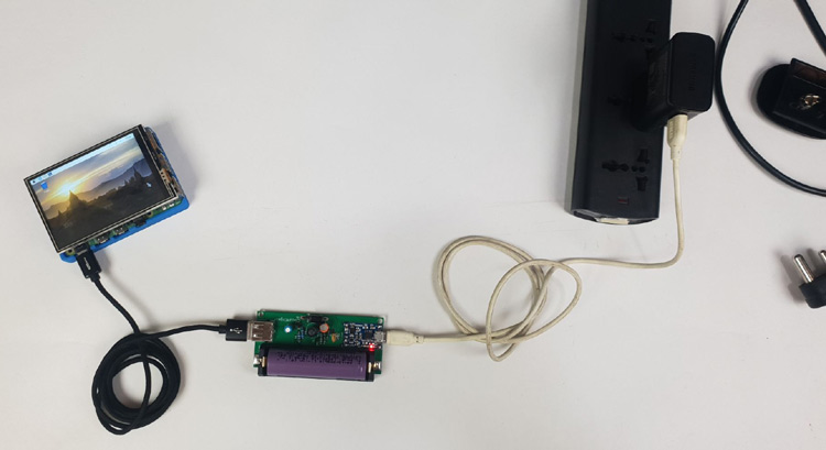
As it can be clearly seen that the Rpi module powers up with the 5V boosted supply from the 3.7V Li-Ion cell. The Red LED can also be observed to be glowing since the cell is currently getting charged and simultaneously providing the supply to the Rpi. Once the cell is fully charged, we would observe a Blue LED, and then we are ready to remove our DC adapter to the TP4056.
For more details and construction, kindly see the video linked at the bottom of this page. Hope you have learned something new today. For more info and questions, please post on the forum section to get a reply. Thank you.
Comments
I'm having problems finding the 6.1k resistor with 1% tolerance for R3. Can you confirm the resistor value?
The value generated by this part of the circuit is used by the FB (feedback) on the MIC2253, according to the datasheet this can be between 1.208v & 1.283. So a 6.1k & 2k gives 1.235v. If you cannot find a 6.1k (yep I tried as well at least for a reasonable price) you are best to adjust R3 & R4 to get the desired voltage. Remember the 1% tolerance as well to calculate the max +/- it will give. A 6k & 2k gives 1.25v and 1% is 1.2375 to 1.2625 so that should be ok. I have tried to get the parts nailed down on this but trying to track between 4/5 suppliers is a pain.
Where is the Schematic file?
What MacOS application will open/edit the Gerber files?
Has anyone managed to build this? I cannot find some of these components anywhere.

How are you getting the low battery voltage signal to the RPi and triggering a soft shutdown? It looks like all you did was create a low wattage powerbank. I would suggest adding a I2C voltage sensor connected to the pi and softwarew that calls shutdown.