

When it comes to designing complex high-density PCBs, layer planning is important for different types of applications. Poor PCB layer stackup management contributes to the poor PCB design and ultimately cause the PCB to malfunction. Layer stackup is a process where lots of things are merged in a simple but calculative way into a single PCB design. To understand layer stacking, it is important to know the different types of layers that are used in printed circuit board design. It is not just simple copper connections that transfer electricity, but it is much more complex in terms of modern PCB routing techniques due to the highly sophisticated components and other parameters. In this article, we thought of clarifying some of the theory and design aspects of common PCB Layer Stack Management techniques that are used for high-density PCB designs.
In our previous PCB articles, we have discussed many PCB design techniques like:
- Basic of PCB
- Via Stitching in PCB Design
- Understanding Blind, Buried, and Through-hole vias in PCB
- How can Teardrops help in Improving Quality and Stability of your PCB Design
You can check those out if you are interested to learn about PCB design and manufacturing. That being said, let's look into the tips to reduce PCB manufacturing costs.
What is Layers Stacking PCB Design?
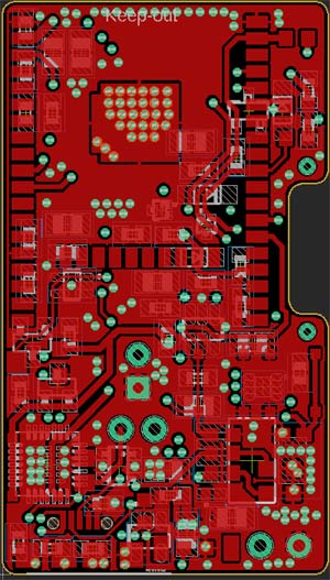
In multilayer board design, mainly three types of layers are used. The layer types are Signal layer, Plane layer, Mixed layers. Signal layers consist of multiple types of signals. The image given below shows a perfect signal layer PCB that has multiple types of signals not depending on special criteria. These are mainly low voltage, low current signals that are mainly used to carry medium to high-speed data lines. This type of layer does not consist of the Ground plane or Power Plane that is made by polygon pour. There is a reason for that. In very high-speed signals, having ground planes or power planes contribute to the impedance changes due to the buildup of stray capacitance as well as stray inductance.
Below image shows a signal layer where multiple signals are routed as well as components are placed.
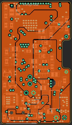
A plane layer is different. It does not consist of any signal other than the Ground or Power Planes. This is useful for multiple reasons, mainly having a good Ground and Power Path all over the circuitry. A solid copper is placed all over the board and by just cutting the copper plane, separate segments are created to provide different plane signals. Below is an excellent example of the same where the Plane layer is shown.
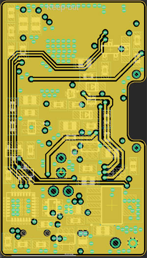
The next type of layer is a mixed layer that uses both signal and copper fill as a plane. This is the most commonly used layer type in two layers and six layers boards. Sometimes it is also used in four-layer boards as well. There are multiple instances that this type of layer is seen in general PCB boards that do not have significantly high-speed traces. The image given below shows an example of a mixed layer type.
How many layers do we need?
The first question arrives before deciding the layer stacking is that how many layers are required for the design. A standard rule of thumb is to use the number of pins on a printed board per unit area.
The below chart can be used as a starting point.
|
Pin Density Ratio |
PCBs layer(s) |
|
more than 1.0 |
1 |
|
0.6-1.0 |
1 or 2 |
|
0.4-0.6 |
4 |
|
0.3-0.4 |
4 or 6 |
|
0.2-0.3 |
8 or 10 |
|
Less than 0.2 |
10 or 12 or 14 |
However, this is not limited to all cases. PCB density depends on components' fixed position, signal integrity, etc. Now, after deciding how many layers should be there, it is time to select the layers for what type of signals to be routed on which layers. Few things are needs to be evaluated before making some decisions.
- It is important to route high current layers on the top and bottom layers. As the internal layers do not dissipate heat through air. Thus, if the internal layers are used for high current operations, it will induce temperature rise of the PCB.
- High-frequency signals emit high EMI, thus internal layers with a stacking of Ground planes on above and bottom layers help to reduce radiated EMI.
Dielectric and Copper Density and Layer Management
Dielectric and copper density are other important criteria that should be taken into consideration for design decisions before making a PCB design. This is because changing the copper density and the dielectric changes the board size and it could alter the impedance parameters of the overall board. The copper density and PCB size are also dependent on the overall cost of the board. Increasing the Board thickness possibly increases the board costing as well.
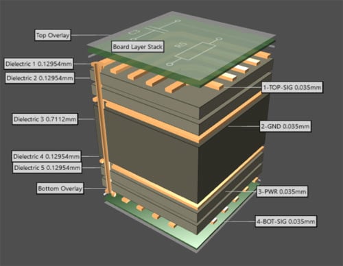
Generally, the copper thickness of 35um and 70um is widely used in PCB layer stack management. Increasing the copper possibly increases the current carrying capacity of the traces and reduces the heat dissipations. A major thing is to select a layer order where the layers are evenly balanced. Below are the most used layers in different layer configurations from 4 layers to 8 layers PCB Board.
4 Layer Stack up:
For optimal performance, the layer assignments need to be exactly as described below. The top and bottom layers can be used for signal layers, and the two internal layers can be used for power and ground this way, we can debug for errors in the PCB.
Layer assignments - Signals (that needs to be tested most often) / GND Plane / Different Power Signals / Signals
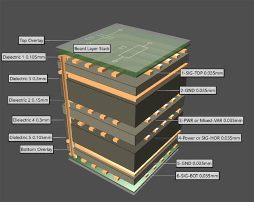
6 Layer Stack up:
For 6 layer PCBs, the process gets a little bit complex but the overall concept stays the same. The signal planes always stay at the top, for any modifications in the POC stage. The ground and power planes live below that and the mixed-signal planes. The power and ground planes are routed vertically and the signal planes are routed horizontally that we reduce EMI and noise for high-speed PCB design. Always remember to make the plane before you start designing the PCB. Thus, if you select the second layer as the Ground plane, always choose the 5 the layer as the ground plane. This is very important. Also, in 6 layer design, route the signals vertically in one layer, and horizontally on another layer. In this case, the magnetic field generated from the traces will cancel each other and reduce the cross talk.
Layer assignments - Signal / Solid GND Plane/ High Speed Signal / High Speed Signal / Solid GND Plane/ Signal
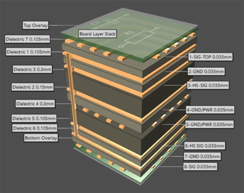
8 Layer Stack up
The concept of 8 layers PCB is also the same, as an 8-layer PCB, it is used for very high-speed designs like computer motherboards, FPGA, and all so to isolate EMI and noise, we put the ground plane below the top and bottom signal plane underneath that, there are mixed signals plane and other ground and power planes. The entire structure is given below.
Layer assignments - Signal / Solid GND Plane/ High Speed Signal / GND or Power / GND or Power / High Speed Signal / Solid GND Plane/ Signal.
This is all about layer stack management. If you have further suggestions or you want to share your layer stack management with us, kindly use our forum.
