
PCB board design basics form the foundation of modern electronics. Whether you're learning PCB design basics for beginners or exploring advanced circuit board design, understanding printed circuit boards is essential for creating reliable electronic devices. Today's circuit board design basics enable everything from smartphones to spacecraft control systems.
Table of Contents
What is a PCB Board? Understanding Circuit Board Design Basics
PCB is a copper-laminated and non-conductive Printed Circuit Board, in which all electrical and electronic components are connected in one common board with physical support for all components with the base of the board. When PCB is not developed, at that time all components are connected with a wire, which increases complexity and decreases the reliability of the circuit. In this way, we cannot make a very large circuit like a motherboard. In PCB, all components are connected without wires; all components are connected internally, so it will reduce the complexity of the overall circuit design. PCB is used to provide electricity and connectivity between the components, through which it functions the way it was designed. PCBs can be customised for any specifications to meet user requirements. It can be found in many electronic devices like: TV, Mobile, Digital camera, Computer parts like: Graphic cards, Motherboard, etc. It is also used in many fields like medical devices, industrial machinery, automotive industries, lighting, etc. PCB board basics start with recognising how these boards eliminate the need for manual wiring, reducing complexity while increasing reliability.
PCB vs. Traditional Wiring
| Feature | Traditional Wiring | PCB Board |
| Complexity | High - manual wire routing | Low - pre-designed traces |
| Reliability | Lower (connection failures) | Higher (permanent connections) |
| Manufacturing Time | Hours to days | Minutes (automated) |
| Circuit Size | Limited scalability | Highly scalable (multi-layer) |
| Cost (bulk production) | Expensive | Cost-effective |
Common Applications of PCB Boards
PCB (Printed Circuit Boards) can be found in virtually every electronic device. The first thing you'll learn about basic PCB design is that it is used in many different applications across many industries.
» Consumer Electronics: There are many consumer electronics, including smartphones, televisions, digital cameras, gaming systems, and smart watches.
» Computer Hardware: There are computer hardware items like motherboards, graphics processing units (video cards), RAM modules, and solid-state drives (SSDs)
» Automotive: Automotive applications like engine control units (ECUs), infotainment systems, sensor packs, and electric vehicle controllers.
» Medical Devices: Medical devices, including pacemakers, diagnostic devices, patient monitoring, and imaging.
» Industrial Systems: Industrial Applications such as automation controllers, robotics, power management systems, and Internet of Things (IoT) sensors.
» LED Lighting: LED systems for smart bulbs, commercial LED lighting systems, or automotive applications.
» Telecommunications: Telecommunications applications, such as routers, modems, cell towers, and satellites.
6 Types of PCB Boards: Complete Guide for PCB Design Basics for Beginners
There are several types of PCB available for the circuit. Out of these types of PCB, we have to choose the appropriate type of PCB according to our application.
- Single-layer PCB
- Double-layer PCB
- Multi-layer PCB
- Flexible PCB
- Aluminium-backed PCB
- Flex-rigid PCB
1) Single Layer PCB:
A single-layer PCB is also known as a single-sided PCB. Single-layer PCBs are the simplest and most cost-effective option for PCB design basics for beginners. Easiest for beginners learning simple PCB layout design. This type of PCB is simple and the most commonly used PCB because these PCBs are easy to design and manufacture. One side of this PCB is coated with a layer of any conducting material. Generally, copper is used as a conducting material for PCBs because copper has very good conducting characteristics. A layer of solder mask is used to protect the PCB against oxidation, followed by a silk screen to mark out all of the components on the PCB. In this type of PCB, only one side of the PCB is used to connect different types of electrical or electronic components like resistors, capacitors, inductors, etc. These components are soldered. These PCBs are used in low-cost and bulk manufacturing applications like calculators, radios, printers and the solid-state drive.

2) Double Layer PCB:
A double-layer PCB is also known as a double-sided PCB. As the name suggests, in this type of PCB, a thin layer of conducting material, like copper, is applied to both top and bottom sides of the board. In PCB, different layers of the board consist of via, which have two pads in corresponding positions on different layers. These are electrically connected by a hole through the board, which is shown in Figure 2 b. More flexible, relatively lower cost, and the most important advantage of this type of PCB board is its reduced size, which makes the circuit compact. This type of PCB is mostly used in industrial controls, converters, UPS systems, HVAC applications, phones, amplifiers and Power monitoring systems. This design is essential for intermediate circuit board design basics.

3) Multi-Layer PCB:
A multilayer PCB has more than two layers. It means that this type of PCB has at least three conductive layers of copper. For securing the board, glue is sandwiched between the layers of insulation, which ensures that the excess heat will not damage any component of the circuit. This type of PCB design is very complex and used in very complicated and large electrical tasks in a very small space and compact circuits. This type of PCB is used in large applications like GPS technology, satellite systems, medical equipment, file servers and data storage. These represent advanced PCB board design basics for complex applications.

4) Flexible PCB:
Flexible PCB is also known as a Flex circuit. This type of PCB uses flexible plastic material like polyimide, PEEK (Polyether ether ketone) or transparent conductive polyester film. The circuit board is generally placed in a folded or twisted form. This is a very complex type of PCB and it also contains a different range of layers like single-sided flex circuit, double-sided flex circuit and multi-sided flex circuit. Flex circuit is used in organic light emitting diode, LCD fabrication, flex solar cell, automotive industries, cellular telephones, cameras and complex electronics devices like laptops. Flexible PCBs use bendable substrate materials like polyimide or PEEK (Polyether Ether Ketone), enabling unique, simple circuit board design solutions for space-constrained applications.

5) Rigid PCB:
Rigid PCBs are made out of solid material, which doesn’t allow the PCB to twist. Same as flex PCB, Rigid PCB also have different layer configurations like single-layer, double-layer and multi-layer Rigid PCB. The shape of this PCB does not change after installation. This PCB cannot be bent according to the shape of the base, which is why this PCB is known as a RIGID PCB. The lifespan of this type of PCB is very high, so this is used in many parts of a computer, like RAM, GPU and CPU. Simple in design, and the most used and most manufactured PCB is a single-sided rigid PCB. Multi-layer rigid PCB can be more compact by containing 9-10 layers. This is the most common type in traditional PCB board design basics.
6) Flex-rigid PCB:
A combination of a Flexible circuit and a rigid circuit is the most important board. Flex-rigid boards consist of multiple layers of flexible PCB attached to several rigid PCB layers. Flex-rigid board is shown in the figure. It is used in cell phones, digital cameras and automobiles, etc. Flex-rigid PCBs combine flexible and rigid board sections into a single integrated design, representing advanced PCB board design basics for high-performance applications.

PCB Board Types Comparison
| PCB Type | Layers | Complexity | Best Applications |
| Single-Layer | 1 conductive layer | Simple | Calculators, LED circuits, radios |
| Double-Layer | 2 conductive layers | Moderate | Amplifiers, UPS systems, HVAC |
| Multi-Layer | 3+ layers (up to 50) | Complex | Computers, GPS, medical equipment |
| Flexible PCB | Variable | Moderate to High | Wearables, cameras, laptops |
| Rigid PCB | Variable | Any | Computer components (RAM, GPU) |
| Flex-Rigid | Mixed | Very Complex | Smartphones, aerospace, automotive |
PCB Mounting Technologies: Through-Hole vs. Surface Mount Design
Understanding component mounting methods is crucial for simple PCB layout design.
- Through-hole PCB
- Surface-mounted PCB
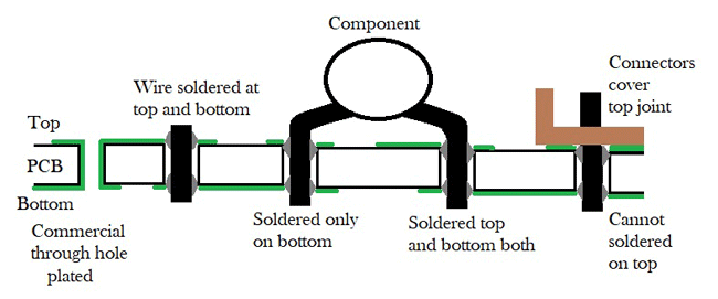
1) Through-hole PCB:
In this type of PCB, we have to make a hole using a drill on the PCB. In these holes, leads of components are mounted and soldered to pads situated on the opposite side of the PCB. This technology is most useful because it gives more mechanical support to electrical components and very reliable technology for mounting components, but drilling in PCBs makes it more expensive. In a single-layer PCB, this mounting technology is easy to implement, but in the case of double-layer and multi-layer PCBs, making holes is more difficult. This traditional method remains important for certain circuit board design basics and applications.

2) Surface-mounted PCB:
In this type of PCB, components are small in size because these components have very small leads or no leads are required for mounting on the board. Here, in this technology, SMD components are directly mounted on the surface of the board and do not require making a hole in the board. SMT dominates modern PCB board design basics for consumer electronics due to its efficiency and compactness.

Through-Hole vs. Surface Mount Comparison
| Feature | Through-Hole Technology (THT) | Surface Mount Technology (SMT) |
| Component Size | Larger with long leads | Compact, minimal or no leads |
| PCB Drilling | Required for every component | Not required |
| Assembly Speed | Slower (manual or semi-automated) | Fast (fully automated) |
| Component Density | Lower | Much higher |
| Mechanical Strength | Excellent | Good (but less than THT) |
| Cost (bulk production) | Higher due to drilling | Lower with automation |
| Best For | High-power, high-reliability applications | Compact, high-volume consumer electronics |
Essential PCB Components and Terminology for Simple Circuit Board Design
Many modern PCB board designs use both through-hole and surface mount technologies. Understanding PCB anatomy is fundamental to PCB design basics for beginners.
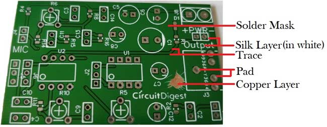
⇢ Pad: Pad is nothing but a piece of copper on which leads of components are mounted and on which soldering is done. The pad provides the mechanical support to the components. In a simple PCB layout design, proper pad sizing ensures reliable electrical connections and mechanical stability.
⇢ Trace: In PCB, components are not connected with the help of wires. All components are connected with a conducting material like copper. This copper part of the PCB, which is used to connect all components that is known as a trace. Trace is like the figure below. Traces are thin copper pathways that replace traditional wires in modern circuit board design basics.
⇢ Layers: According to the application, cost and available space of the circuit, the user can choose the layer of PCB. Most simplest in construction, easy to design and most useful in routine life is the single-layer PCB. But for very large and complex circuits, double-layer PCB or Multi-layer PCB is most preferred compared to single-layer PCB. Nowadays, in multi-layer PCBs, 10-12 layers can be connected, and the most critical thing is to communicate between the components on different layers. Understanding layer stackup is essential for advanced PCB board design basics.
⇢ Silk layer: The Silk layer is used for printing lines, text or any art on the surface of the PCB. Usually, for screen printing, epoxy ink is used. Silk layer can be used in the top and/or bottom layer of PCB according to the user's requirement, which is known as silk screen TOP and silk screen BOTTOM.
⇢ Top and bottom layer: In the Top layer of the PCB, all components are mounted in this layer of PCB. Generally, this layer is green coloured. In the bottom layer of PCB, all components are soldered through the holes and the leads of the components are known as the bottom layer of PCB. Sometimes, in the top and/or bottom layer, PCB is coated with a green colour layer, which is known as solder mask.
⇢ Solder Mask: There is one additional layer on the top of the copper layer called Solder Mask. This layer generally has a green colour, but it can be of any colour. This insulating layer is used to prevent accidental contact of pads with other conductive material on the PCB. This essential layer prevents solder bridges during assembly—a key concept in PCB design basics for beginners.
PCB Materials Guide: Choosing the Right Substrate for Your Circuit Board Design
The main element is a dielectric substrate, which is rigid or flexible. This dielectric substrate is used with a conducting material, like copper, on it. As a dielectric material, glass epoxy laminates or composite materials are used. Aluminium PCBs use a metal substrate for superior heat dissipation, essential for high-power simple circuit board design applications.
1) FR4:
FR stands for FIRE RETARDANT. For all types of PCB manufacturing, the most common glass laminated material is FR4. Based on woven glass-epoxy compounds, FR4 is a composite material which is most useful because it provides very good mechanical strength. Understanding FR4 is essential for PCB design basics for beginners.
FR4 | Glass transition temp. |
|
Standard | 130 |
|
With higher glass transition temp. | 170-180 |
|
Halogen free | -- |
|
2) FR-1 and FR-2:
This material is made from paper and phenol compounds, and this material is used for only single-layer PCBs. Both FR1 and FR2 have similar characteristics; the only difference is the glass transition temperature. FR1 has a higher glass transition temperature compared to FR2. These materials are also subdivided into standard, halogen-free free and non-hydrophobic. FR1 and FR2 use a paper substrate with phenolic resin, offering a lower cost for simple PCB layout design projects with minimal requirements.
3) CEM-1:
This material is made from paper and two layers of woven glass epoxy and phenol compounds, and this material is used for single-sided PCBs only. CEM-1 can be used instead of FR4, but the price of CEM-1 is higher than FR4. CEM (Composite Epoxy Material) boards blend paper core with glass fiber surfaces, balancing cost and performance in PCB board design basics.
4) CEM-3:
This material is a white coloured, glass epoxy compound, which is mostly used in double-layer PCBs. CEM-3 has lower mechanical strength compared to FR4, but it is cheaper than FR4. So, this is a good alternative to FR4.
5) Polyimide:
This material is used in a flexible PCB. This material is made from Kepton, Rogers, dupont. This material has good electrical properties, flexibility, a wide temperature range and high chemical resistance. Working temperature of this material is -200 ͦC to 300 ͦC. Polyimide is the premier material for flexible PCBs, offering exceptional thermal and chemical resistance crucial for advanced circuit board design basics.
6) Prepreg:
Prepreg means pre-impregnated. It is a fibreglass impregnated with resin. These resins are pre-dried, so that when it heated, it flow, stick and completely immerse. Prepreg has an adhesive layer which gives strength similar to FR4. There are many versions of this material according to resin content: SR- standard resin, MR- medium resin and HR- high resin. This is chosen according to the required thickness, layer structure and impedance. This material is also available in high glass transition temperature and halogen-free. Prepreg (pre-impregnated) fibreglass provides the adhesive layers in multi-layer PCB board design basics, bonding copper layers together.
Best PCB Board Design Software: Complete Guide for Beginners and Professionals
Choosing the right PCB board design software is critical for efficient circuit development. Modern CAD tools transform schematic concepts into manufacturable board layouts. Here's a comprehensive guide to the top PCB design software options. Below are some of the most popular PCB design software. You can know more about these PCB design software here.
Eagle:
EAGLE is the most popular and easiest way to design PCBs. EAGLE stands for Easily Applicable Graphical Layout Editor, which was previously developed by CadSoft Computer, and currently, Autodesk is the developer of this software. For designing a circuit diagram, EAGLE has a schematic editor. The EAGLE file extension is.SCH and different parts and components are defined in.LBR extension. The board file extension is.BRD. EAGLE remains one of the most popular PCB board design software choices for learning PCB design basics for beginners.
Multisim:
Multisim is also a very powerful and easy learning software. Which is originally developed by Electronics Workbench and now it is a division of National Instruments (NI). It includes microcontroller simulation (MultiMCU) and integrated import export features to the PCB layout software. This software is widely used in academia and also in industry for circuit education. Multisim, developed by National Instruments (NI), emphasises circuit simulation alongside PCB layout, making it excellent for educational PCB board design basics.
EasyEDA:
EasyEDA is a software which is used to design and simulate circuits. This software is an integrated tool for schematic capture, SPICE circuit simulation, based on Ngspice and PCB layout. The most important advantage of this software is that it is a web-based software and is used in a browser window. So, this software is independent of the OS. EasyEDA revolutionises accessibility as a completely browser-based PCB board design software, requiring no installation—ideal for learning simple PCB layout design anywhere.
Altium Designer:
This software is developed by the Australian software company Altium Limited. The main feature of this software is schematic capture, 3D PCB design, FPGA development and release/data management. This is the first software which offers 3D visualisation and clearance checking of PCB directly from the PCB editor. Altium Designer is the industry-leading professional PCB board design software, offering unmatched capabilities for complex circuit board design basics and advanced applications.
KiCad: This software is developed by Jean-Pierre Charras. This software has tools which can create a BOM (Bill of Materials), artwork and 3D view of PCB as well as all components used in the circuit. Many components are available in the library of this software, and there is a feature that user can add their custom components. This software supports many human languages. KiCad is a completely free, open-source PCB board design software with no limitations, making it ideal for both beginners and professionals learning circuit board design basics.
CircuitMaker: This software is also developed by Altium. The schematic editor of this software includes basic component placement, and this software is used to design advanced multichannel and hierarchical schematics. All schematic is uploaded to the server, and these files are available to view by anyone, provided that you need a CircuitMaker account.
PCB Board Design Software Comparison
| Software | Best For | Pricing | Platform | Key Feature |
| EAGLE (Autodesk) | Beginners, hobbyists | Free (limited), Paid | Windows, Mac, Linux | Easy learning curve |
| KiCad | Open-source enthusiasts | Free (fully featured) | Windows, Mac, Linux | No restrictions |
| Altium Designer | Professional engineers | $$$ (subscription) | Windows | 3D visualization |
| EasyEDA | Quick prototypes | Free, browser-based | Web browser | No installation needed |
| OrCAD | Enterprise design | $$$ (license) | Windows | Industry standard |
| Multisim | Education, simulation | $$ (educational), $$$ | Windows | Integrated SPICE |
| CircuitMaker | Community projects | Free | Windows | Cloud collaboration |
Frequently Asked Questions: PCB Board Design Basics
⇥ 1. What material is used in the construction of a PCB?
FR4 is the most commonly used PCB material, which consists of woven fibreglass with epoxy resin. It exhibits good mechanical strength, good electrical properties, and low cost. Alternatives are FR1/FR2-paper-based, CEM-3, polyimide for flexible circuits, and aluminium-backed boards for high temperatures, such as LEDs.
⇥ 2. What is the difference between through-hole PCB technology and surface mount technology?
THT technology includes drilling holes that allow leads to be inserted into the PCB, and since they have versus, THT-SMT technology includes placing components directly onto the surface of the PCB board, without drilling holes, thus allowing smaller components and automatic assembly. SMT is predominant in modern electronics due to its advantages relative to THT technology, which is limited to components that draw high-current of power and are under mechanical stress.
⇥ 3. How to Determine the Trace Width Of a PCB for a Given Current Rating?
The trace width is determined by the current, the thickness of the copper, and the temperature rise. A good rule of thumb is that for 1oz copper, a 0.25mm trace will be rated for approximately 1A. You can obtain a more precise trace width rating using the internet-based trace width calculators, which calculate trace width using the IPC-2221 standard. You will enter the current rating you want to achieve, the copper thickness, 1oz or 2oz, and the acceptable rise in temperature, which is usually 10 °C for a safe PCB board design.
⇥ 4. What is a via in PCB design, and when would I use a via?
A via is an electroplated hole that provides electrical connectivity between copper traces that are located on different layers of a PCB. Vias are necessary in routing between layers, specifically in multilayer boards, and to connect the top/bottom in a double-layer design. The standard diameters for standard vias are 0.3 - 0.6mm. I recommend you limit the number of vias in your PCB layout design in order to keep your manufacturing complexity low, as each via only adds a potential failure point to your PCB.
⇥ 5. What is a solder mask, and why is it important?
A solder mask is a polymer coating that is usually green, which is placed to cover copper traces but expose pads. It protects the copper from other solder on the board that could cause bridges while soldering, it seals in solder masks from oxidising, and it provides electrical isolation between traces. Solder masks are an essential component of PCB design based on simple principles that would ensure reliability during manufacturing and longevity.
⇥ 6. How many layers do I need in my PCB board design?
The number of layers will depend on the complexity of the circuit and board. If the circuit is very simple, then you can use a single-layer board: LED drivers, simple sensors. A double-layer board will be good for medium complexity: Arduino shields, amplifiers. It is common to use four layers for digital circuits (signal-ground-power-signal). Use six layers or more for high-speed, RF, or very dense designs. It is best to start simple and only add layers when you have to for routing or signal integrity.
⇥ 7. Which file format should the PCB manufacturer require to be able to manufacture the PCB?
Fabrication requires Gerber files (RS-274X format) that include all copper layers, solder mask, silk screen, and drill data. Most PCB board design software is able to export Gerber files directly. Also included should be Excellon drill files and a fabrication drawing that shows dimensions, layer stackup, material specifications and special requirements.
⇥ 8. What are the most common PCB design mistakes beginners make?
Some common mistakes are trace width being too small, leading to overheating; poor clearance of traces, leading to shorts; decoupling capacitors missing near ICs; poor design of ground planes, leading to increased noise; and ignoring the DRC errors. Always validate your designs, apply the manufacturer's DRC rules, and review the datasheets to implement the basic principles of PCB board design.
Conclusion: Mastering PCB Board Design Basics
Grasping PCB board design basics is your first step towards creating professional electronic equipment. From the simple PCB layout design of single-layer boards to the more complicated and multi-layer high-speed circuits, you will find the basic principles of circuit board design basics in my comprehensive guide, which will help you on the path to your development project.
Whether it is selecting the right PCB type, selecting through-hole or surface mount technology, selecting PCB materials, like FR4 or polyimide, or learning PCB board design software, like KiCad or EAGLE, the basics are often the first principles of designing a successful electronic product.
Key Takeaways for PCB Design Basics for Beginners:
∗ Start with an easy, single-layer design and work towards difficult, multi-layer boards
∗ Select PCB Materials, based on the requirements of your application, for example, FR4 when working with general-purpose designs, aluminium when working with high-power LED designs
∗ Learn free software like KiCad or EasyEDA before purchasing expensive professional software
∗ Always follow design rule checks (DRC) as a best practice to eliminate issues during manufacture
∗ Take into consideration both electrical and mechanical aspects when designing your circuit board
Start your PCB design journey today! Explore our related tutorials on schematic capture, component selection, and PCB assembly techniques. Master simple circuit board design step by step, and soon you'll be creating professional-quality electronics. This tutorial was created by the Circuit Digest engineering team. Our experts focus on creating practical, hands-on tutorials that help makers and engineers master Raspberry Pi projects, Arduino projects and IoT development projects.
I hope you liked this article and learned something new from it. If you have any doubts, you can ask in the comments below or use our Circuit Digest forum for a detailed discussion.
Projects Using PCB
Previously, we have used PCBs to build many interesting projects. If you want to know more about those topics, links are given below.

Design and Build a Compact 3.3V/1.5A SMPS Circuit for Space Constraint Applications
In this project, we will build a compact power supply with a 3.3V, 1.5A power rating, which serves the purpose. To build this SMPS circuit on PCB, we had our PCB boards from PCBWay, and we assembled and tested the same in this tutorial session.

Digital Wall Clock on PCB using AVR Microcontroller Atmega16 and DS3231 RTC
In this Digital Clock Project, ten common anode 7-segment displays of 0.8-inch are used to display time and date. Here, seven seven-segment displays are used to show hour, minute, date, month and year. Our PCB design also has options to display seconds and temperature, which can be displayed by adding more display units.

How to Build a Precision Digital Micro Current Meter with STM32
The Precision Digital Micro Current Meter is a purpose-built hardware solution designed to accurately measure extremely low current levels in embedded and battery-powered systems.
This is very informative... thanks
Your article is helpful and looked concise and complete.
This is very good information
Your sharing is very detailed, thank you!

Thanks it's very helpful.