
When PCBs were not discovered, engineers connected all components on a circuit using external wires similar to how it is done on a breadboard today. But as the circuits became larger and more complex it became extensively hard to build reliable connections using externals wires. To solve this issue, PCBs were introduced back in the year 1936. Today there are many tools and software available online and offline for PCB designing that can help you design and fabricate PCBs with ease. We have already learned about the Basics of PCB in our previous article, in this article, we will discuss and compare some popular PCB designing software for their price, usability and other features. Here we are discussing some most commonly used EDA software like EAGLE, Multisim, EasyEDA, Altium design, OrCAD, and KiCAD. These software are widely used for PCB designing and simulation of the electronics circuit.
Eagle:
The most popular and common CAD software for PCB designing is EAGLE. EAGLE stands for Easily Applicable Graphical Layout Editor. This software was developed by CADSoft Computer in 2016, today EAGLE is procured and maintained by AUTODESK.
EAGLE has a very simple, effective and easy interface and provides a library that contains a large number of electrical and electronics components. That is the main reason for EAGLE being the most popular PCB designing software among educationists, hobbyists, and professionals. EAGLE can be installed on Windows, Linux and MAC platforms. On top of all this, the free version of this software is available for download on AUTODESK website.
Eagle has two editors; Schematic editor and PCB layout editor. The schematic editor is used to add all components and connect according to the circuit requirement. This schematic file has unique features like modular design block, multi-sheet schematic, electronic rule checking and real-time design synchronization. After this, schematic is directly converted into PCB layout editor, in which we can set components according to less complexity. This PCB layout editor also has some good features like alignment tools, obstacle avoidance, routing engine. These features are available in free version.
For professional use, EAGLE provides paid version which is available at 1000$/year. In this paid version, AUTODESK provides technical support that includes call, mail and online chat support and also provides access to latest software release. But for an educational and self-use, the free version of this software will just do more than good.
When you install the free version of EAGLE and open it, the first page is a control panel as shown in the below figure.
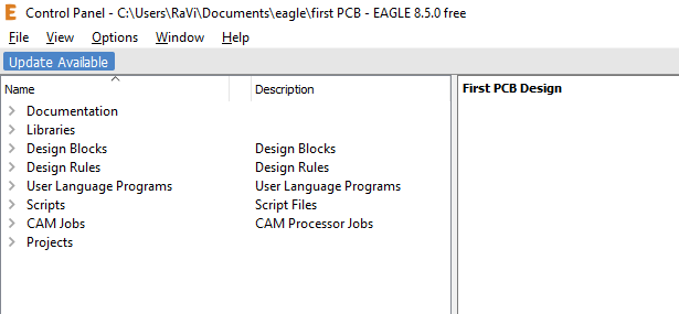
As shown in the above figure, the folder name and description of that folder or file are given. First is Documentation which contains some tutorial documents followed by that we have Libraries (.lbr), which contain a large list of electrical components. If you ever need more components, they can be quickly downloaded from a quick Google search and added into the library folder. Next is the design block (.dbl), where you can find some inbuilt design for most common circuits that you can directly add to your project. Design rules (.dru) contain rules for track, drill and final copper with important notes and information. Next is User Language Programs (.ulp) which is used to access data structure and to create an output file, the user can also build their own ULP file if required. Next is Scripts (.scr), which contains text files with eagle commands and it is very useful for automating a task like drawing a pattern, change of track width, etc. CAM jobs (computer aided manufacturing) (.cam) contains some standard CAM files and the last one is Projects which contains a list of the project with schematic and PCB layout file made by the user.
You can also make a Gerber file with the help of eagle. Gerber file is a universal language for PCB designing and this is the last step of PCB designing.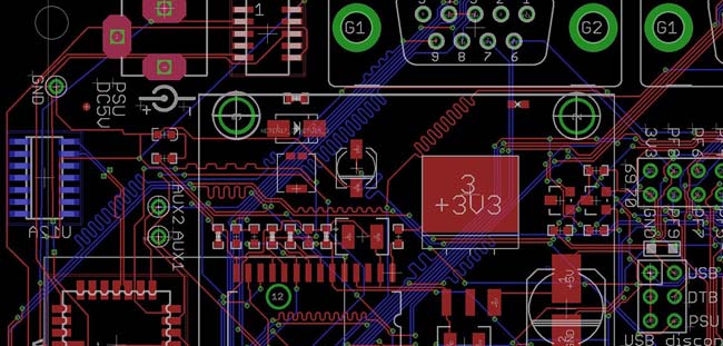
Multisim:
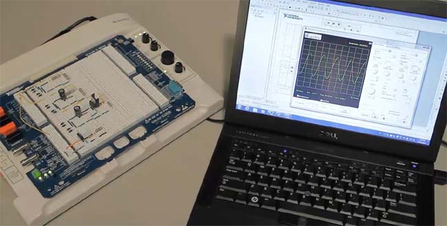
Multisim is famous among students and researchers because it contains powerful circuit design software with good simulation capabilities that can be useful for research and teaching applications. Multisim has an advanced, powerful and industry-standard SPICE simulation environment that is popular for its unique features and easy to use design. If you compare Multisim with eagle, the main advantage of Multisim is that it has a simulation environment which is not available in eagle but if you compare for only PCB designing purpose, eagle can be considered as a better platform compared to Multisim.
Multisim was developed by electronics workbench and interactive image technology. During the early days, this software was just used to teach electronics programs in colleges, it was not much used for industrial applications. But after some time when National Instruments added some new features, it became widely accepted by professionals and educators. Multisim is available in two variations; one is made for students and educators and the second is made for professionals and industrial purposes.
Multisim enhances powerful simulation technology with the ability to analyze analog, digital and power electronics circuits for education, research, and design purposes. This software has some unique functionality like parameter analysis, integration with new embedded targets and simplified user design templates. With Multisim Standard Service Program (SSP) customers can also have access to self-paced online training modules. You can download the Multisim trial version from here to get started.
EasyEDA:
EasyEDA is a web-based Electronic design automation (EDA) tool. It is a web-based tool, so there is no requirement to download or install any software. To use EasyEDA, you have to open easyeda.com from any HTML5 capable web browser. It doesn’t matter which OS you are using, because it can support windows, Linux and MAC. All you need is a web browser like Chrome, Firefox, Safari, Internet Explorer or Opera but it is recommended to use this in chrome or firefox for better performance. Being an online open-source tool, is the biggest advantage of EasyEDA.
EasyEDA is simple, user-friendly and is a very good platform if you don’t have much knowledge about PCB designing. It can uses anywhere, anytime and from any device, all you nned is to log in to your account and start designing. One advantage of this site is, it has large numbers of open source projects, which is easily available from the internet and also very good tutorials are available in EasyEDA official website. We have also developed many PCB Projects using EasyEDA here at CircuitDigest. It has more than 500000 libraries with symbols and footprints of components and you will ever need, there is also a feature to create your own component symbol and footprint if needed. One more advantage is, it can support other software libraries and schematic which includes Altium, EAGLE, LTspice, and DXF.
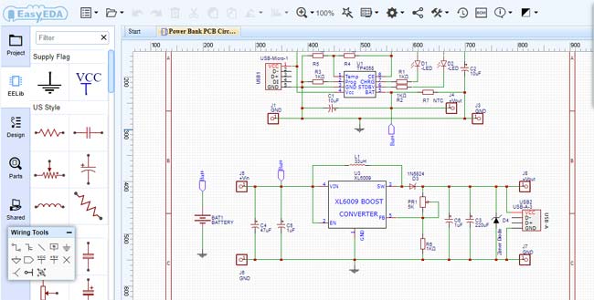
When you open https://easyeda.com/editor this link, it will look like the below screenshot. In this editor you can find navigation panel, toolbar, workspace, drawing tools, writing tools and many more functions. Let’s start with navigation panel which contains EELib, design, Parts, Shared, LCSC.
EELib is the EasyEDA libraries that provide lots of components.
Design is a design manager that is used to check each component on the net easily.
Parts contain schematic symbols and PCB footprints.
Shared if someone sends their project to you than this will appear in the shared tab.
LCSC: If you want to buy components to finish your PCB project, you should try another website LCSC.com
Drawing toolbar: Sheet setting, line, image, Bezier, arc, text, freehand draw, arrowhead, rectangle, polygon, ellipse, pie, drag and canvas origin.
Wiring toolbar: wire, bus, bus entry, netlabel, net flag VCC, net flag +5V, net port, net flag ground, voltage probe, pin, group/ungroup symbol.
Altium:
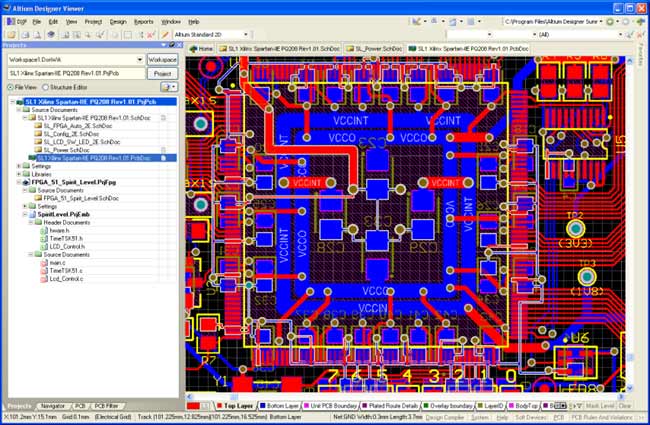
Altium Designer is a commercial electronics design package for Windows. The Altium Designer UI follows modern design standards that allow engineers to perform complex tasks quickly and efficiently. And a major update of the software is available every year, which delivers expanded capabilities, in addition to regular bug fix releases throughout the year.
Altium Designer contains the schematic and PCB Layout tools that you will ever need in one application. This unification allows a user, or team of users, to progress a project from idea to manufacturing in one package. Altium has many advanced features targeted at collaborative work by teams of engineers which also includes some extensive integration with popular mechanical CAD tools on the market. This integration allows the entire product development team to work on the product together.
The software features full 3D capabilities during PCB design and provides enhanced visibility of the design and routing with high-quality screenshots of board designs in progress. The 3D capabilities also help in Design rules check to ensure correct clearances between 3D models of components on the board and between 3D modeled parts and imported enclosures which reduces the risk of surprises during manufacturing. The hardware-accelerated 3D engine also allows seamless design integration of multi-board projects, as well as boards integrating rigid-flex elements.
Schematic capture in Altium is so quick and painless, making the software highly time saving by bringing sophisticated designs to completion. Engineers can interactively route entire busses at once, allowing manual control with intelligent guidance from the software. Design rules are applied in real-time as you route the traces on a PCB, which prevents short-circuiting tracks or otherwise creating design rule violations. One of the interactive routing modes in Altium Designer called ‘Hug and Push’ will intelligently move traces out of your way as you try to route through gaps, while also maintaining a minimum clearance to other nearby traces. When you are routing high-speed designs, such as USB3.0 or DDR, Altium Designer has full support for differential pairs and interactive tuning of net lengths.
When it comes to having your board manufactured, Altium Designer has the ability to build a panel of boards for production rapidly. The Draftsman tool allows quick production of mechanical and assembly drawings of the board for assemblers. Altium Designer integrates fully with Octopart making it possible to create a live bill of materials that associates components in the design with real-world supplier parts. This association will enable you to rapidly source parts from the lowest priced supplier - taking hours out of the component procurement stage, while also ensuring there are no obsolete or poorly stocked components in the design.
For hobbyists and very small businesses, Altium also offers lower cost and free software with a reduced feature set, mostly removing the features targeted towards sophisticated or very intricate designs. These are:
- CircuitStudio, a much lower cost PCB design package that has many of the Altium Designer features.
- CircuitMaker, a free version for open source projects.
- Altium Upverter, a free web-based tool targeted towards makers/hobbyists.

KiCAD
KiCAD is a popular software for electrical design automation and it does not require any license hence it is completely free to use PCB Design Software. Documentation of this software is distributed under two choices; GNU General Pubic Licence and Creative Common Attributes. KiCAD is freely available software, but for new development, they accept money as a donation if anyone wants to donate, otherwise it is free for all users. The setup of this software and libraries are easily available from its website. You can download the KiCAD and its libraries from its official website.
KiCAD is developed by jean-pierre charras. This software can also be used to create a BoM (Bill of Materials), Gerber file and it also provides 3D layout of the PCB. KiCAD also has it's own library, which contains most of the electrical components. This software is also available in 19 different languages and it can run in Windows, Linux and MAC.
KiCAD is divided into five parts;
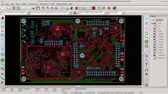
KiCAD that is project manager; Eeschema is the schematic capture editor; pcbnew that shows the layout of PCB in both 2D and 3D; gerbfile is used to generate Gerber file; bitmap2component can convert images to footprint.
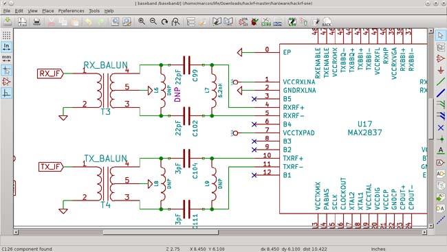
Out of these parts, Eeschema and pcbnew are the most used options. Eeschema has features like custom symbol creation, electrical rule checking, and hierarchical schematic sheets. In PcbNew, it provides a very easy way for routing the components and makes it easy for troubleshooting the PCB Design. if you want to change any vias, hole, trace or any other components of PCB, it is easy in KiCAD compared to other software. After you have designed your PCB, you can check your design in interactive 3D view. Eeschema and pcbnew also supports EAGLE files. If you are new with KiCAD, tutorials are also given in PDF format in many languages and also video tutorials are also available on their website.
Overall software is good for beginners and the biggest advantage is that this software is freely available. So, one does not require to purchase any licence. You can download the KiCAD from here.
OrCAD
The name of this software came from the name of the company Oregon. OrCAD = Oregon + CAD. This software is not freely available, the price of it's license version is starting 2300 USD. OrCAD is developed by John Durbetaki, Ken and Keith Seymour.
OrCAD is divided into two parts; OrCAD Capture and PSpice. OrCAD Capture is used to design circuits and this part is known as PCB suite. OrCAD provides three types of PCB suites; OrCAD Standard, OrCAD Professional and Allegro PCB. OrCAD standard is a concept to production design environment and price of this is starting from 1300 USD. OrCAD Professional has professional-grade PCB design capabilities. This version is costly compared to the standard version and costs around 2300 USD. Allegro PCB is used for expertise level PCB design.
OrCAD PSpice is used for simulation and verification for circuit. PSpice is stands for Personal Simulation Program with Integrated Circuit Emphasis. Capture and PSpice make complete simulator and PCB designing tool. PSpice is also available in two versions; PSpice Designer and PCB Designer plus. PSpice Designer is for industry-standard simulation and contains 33000 parts in the library. This version is starting from 1980 USD. PSpice designer plus is to analyze for reliability, cost, and yield. This version has all features of PCB designer and other unique features like cost analysis, yield analysis, design optimization, system C/C++ modeling and simulation, reliability analysis and HW/SW co-simulation.
OrCAD PSpice can simulate a circuit that is designed in capture and it also can simulate design from MATLAB/Simulink. This feature makes OrCAD unique from all other software. You can download the trial version of OrCAD from here.
Conclusion:
Out of all these software, Eagle provides the best results for PCB designing. If you are a professional PCB designer and your application is very large and complex then go for Altium designer. If you are beginner and just starting with PCB designing than go for EAGLE or EasyEDA, because you will find very good resources and tutorials from the internet which is very helpful if you are a beginner. If you need it in a Company and don’t want to purchase any license then use KiCAD.
Eagle subscription is US$ 100/year not US$ 1000
Glad you pointed it out, even I got a little suspicious over there
Poorly written article. Come on! EAGLE is one of the most ridiculous PCB design tools to use. The GUI and UX and component creation is a nightmare. Most PDC design tools use the common graphical editing paradigm where you select an object and you can drag/move/rotate it right away. Or for deleting an object you usually select it and then press Delete on your keyboard. But in eagle you have to use a separate tool for rotating and moving and deleting. Such a waste of time.
The great ease of Eagle is the use of short-keys which are all custom definable. With your left hand on the function keys and right-hand on the mouse, you can make a PCB-layout much faster and easier then in Altium!
Furthermore the portability of a Altium design to a different computer (at home) is very bad. The stupid use of libraries is to complicated in Altium.
The biggest mistake in Altium is to put all component parameters inside the Altium Library! As if it were an ERP .....!
So I'd say Altium is very un-flexible in use. I think it was made for project managers to show how well everything is integrated: 3D, BoM, ODB+ etcetera.
But end of the day we use a 3D Cad program like solid-works or similar for 3D, and Excel in combination with an ERP for BoM. So to integrate this into one software is a dumb decision in my opinion!
Are kicad gives me the same file of proteus
altium is another premium schematics and PCB design software. Developed by Australian software company Altium Limited, it is one of the most popular PCB design tools among core professionals.
I recommend a PCB and PCBA factory, KingCredie Technology Limited.
They have advantage in low/mid volume PCB and PCBA productions.
Whoops - do your research please, with respect to the elderly : ) Eagle CAD has not been developed in 2016, but in 1988, more than 30 years ago.
In a good way its describing best pcb design software but fusion 360 could be added to list also

What about fritzing ?