PCB Design

|
The Role of AI in PCB Design - Will Engineers Be Replaced? The world of printed circuit board (PCB) design is changing fast and artificial intelligence (AI) is one of the major… |

|
DIY Mini ESP32 Handheld Gamepad: A Compact Retro Gaming Experience If you love retro games and enjoy DIY electronics, this project made by YK Electrical is perfect for you. It’s a tiny handheld gamepad powered by… |

|
DigiKey Announces Sponsorship of KiCad to Support Open-Source EDA Development THIEF RIVER FALLS, Minnesota, USA – DigiKey, a leading global commerce distributor offering the largest selection of… |

|
Linux-Based Drum Kit Business Card An experienced embedded systems developer Sergey Antonovich has developed a business card that integrates a Linux… |

|
Tobor Robotics - Open Source, Modular, Highly Customizable Platform for Automation and Robotics Evezor has introduced Tobor Robotics, a highly customizable and modular open-source robotics platform ideal for desktop… |

|
Building Tiny Battle Bot with ESP8266 An electronics enthusiast recently shared an impressive project called Tiny Battle Bots, inspired by the popular… |

|
Altium Acquires Part Analytics to Strengthen Electronics Supply Chain Management Altium, a global company specializing in electronic design systems announced the acquisition of Milwaukee-based Part… |

|
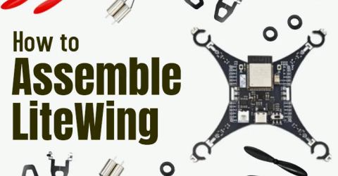
How to Assemble LiteWing Drone?Introduction
If you've received the DIY version of LiteWing, follow these simple steps to assemble your drone. No 3D-printed frame or complex… |

|
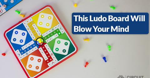
Build a Smart Digital Game Board Using Multicolour PCB Ludo, one of our cherished childhood board games, holds a special place in our hearts. Its simple yet engaging gameplay… |

|
RP2040 Business Card: Playing Doom on a Tiny PCB What if your business card could do more than share contact information? A community creator has made an RP2040-powered business card capable of… |

