Working with High Voltage Electronic Designs? Here is What You Should Know

Submitted by Staff on Thu, 08/04/2022 - 15:42

For engineers who spend their design time in the single-digit, low-voltage world, the phrase "high voltage" may conjure up voltages in the double digits, perhaps as high as 24V or 48V DC, or even the triple-digit domain of line voltages of 120/240 VAC. Yet there's a huge and essential world of engineering design that must be done at 1000V, 1500V, and higher voltages.

Designing products for this region calls for very different thinking, component selection, and interconnection, often in areas designers of low-voltage products do not have to even consider. These concerns apply to passive components, connectors, wiring interconnects, MOSFETs/IGBTs, layout, and of course, safety and regulatory issues. It's a difficult, unforgiving world when your voltage potentials are that high. Trivial oversights can suddenly become major equipment- and life-threatening events. Remember: Rule number 1 is to stop and think before you do anything; rule number 2 is invoke rule number 1 again, perhaps several times.

The Need for High Voltage

Given the challenges and risks, why do design engineers even consider using these voltages at all? It's either because the engineer has no choice, or because it's a really good and necessary idea. The applications fall into two broad groups:

In the realm of "the engineer has no choice," scientific, medical, and physics instrumentation need high voltages in specialized equipment such as X-ray machines, to develop high-intensity fields, ionize atoms, and accelerate electrons and other particles. The same applies to vacuum tubes that still need high-power broadcasting or even moderate-power microwave and mm-wave transmitters. In a more common application, even a commercial neon sign needs several kV to ionize the noble gases inside. Note that many of these applications require kilovolts and more but at relatively modest currents of around 100mA.

Many scientific experiments need potentials of thousands of volts at low current to stimulate particles, or control and accelerate their motion.

In cases where using high voltages is a "really good and necessary idea," engineers are designing for power and efficiency. When a power supply or motor needs to produce large amounts of power, the source must deliver watts, which are the product of voltage and current. But at lower voltages the currents are obviously higher, so IR (current X resistance) losses in conductors, connectors, switches, and active devices cause inefficiency, losses, and I2R heating.

High Voltage designing for very high voltage

To minimize IR losses in cables, connectors, magnetics, and active components, motors are designed to operate from mains at very-high voltages.

The way to minimize these losses is to increase the voltage and thus reduce the current, thereby reducing IR losses and I2R heating. That's why, for example, electric locomotives operate at 20 kV and power-company AC-feeder lines can run at 100 kV and more. If we were to operate this kind of equipment at lower voltages, basic line and other losses- both as efficiency cost and dissipation of heat- would be significant and could not be tolerated. In contrast to the scientific, medical, and physics instrumentation applications cited above, these "power delivery" designs can be at tens or hundreds of amps, in addition to their kilovolt rating.

Start With Physical Dimensions

Dealing with high voltage begins with conductor spacing and associated dimensions. The critical terms for spacing conductors at higher voltages are creepage and clearance.

  • Creepage is the distance an arc may travel measured over a surface, such as between two traces on a printed-wiring board or across the surface of a connector or IC.
  • Clearance is the shortest distance an arc may travel through air, such as from the pin-to-pin of a connector or IC.

The creepage and clearance requirements are a function of the peak voltage; for a sine-wave AC signal, the peak value is 1.4 times the RMS value, plus a substantial safety factor. While it would be nice to be able to call out specific creepage and clearance dimension requirements at any given voltage, it is not possible to do so because their dimensions depend on many factors:

  1. Whether it is a potential shock hazard or only a functional-breakdown issue,
  2. The region of the world: different zones have different standards,
  3. The application: scientific, industrial, or medical, for example, or even a consumer product,
  4. Maximum operating altitude and humidity (dry air at sea level has a flash-over rating of about 4kV /cm, or 10kV/inch),
  5. Across PC boards and other surfaces: the degree of potential contamination that may be expected due to various kinds of pollution; the PCB material group; and the coating (if any).

Therefore, some serious research is needed to determine the required minimum creepage and clearance values, or engineers may need to call an experienced consultant, especially if the end product will need formal regulatory approval for manufacturing and sale.

Move On to Passive Components

Designers who work at lower voltages rarely need to look at the voltage ratings of their basic passive components; those almost countless resistors, capacitors, and inductors that support ICs and discrete devices. Yet each of these does have a maximum working voltage rating specification. Above this voltage, the component may not work to specification, may "gracefully" degrade, fail prematurely, or suffer catastrophic failure.

For example, a capacitor may be specified as "10μF/15 VDC," a voltage rating at the maximum it should ever be allowed to see. Note that the question of how long it can tolerate this overvoltage depends on the vendor; it may be as short as milliseconds or as long as minutes, so engineers must look at vendor definitions. If used at 100V, it is likely that there will be arcing between internal layers of the capacitor, shorting them out and destroying the capacitance function. Most designers like to work with a safety factor of two to three times their expected maximum voltage, so a designer of a 1-kV DC circuit would select passives rated for 2 to 3kV.

For example, the AVX SXP style molded, radial, multilayer capacitor (Fig. 3) comes in a variety of maximum-voltage ratings, up to 3000 V. The largest member of the family, SXP4, is available from 100pF to 2200pF, and measures 22.4 × 16.3 × 5.84-mm thick, with lead spacing of 19.8 mm (about the length of a standard paper clip.)

capacitor

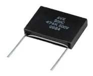
This capacitor in the AVX SXP series is rated to 3000V, and has a lead spacing of just under 20 mm.

Connectors and Cables

What about connectors and cables? Although they are often not considered along with "passive" components like resistors, capacitors, and inductors, they are also a critical link in the high-voltage chain and have many of the same parameters as basic passive components. As with layout and wiring, creepage and clearance are primary factors when choosing high voltage interconnects. But there is a difference between the issues in wiring and layout compared to connectors and wires: circuit and system designers do not typically design connectors; they buy them. Whether a standard, off-the-shelf part, or a custom-designed one, it is the connector manufacturer who determines and defines the voltage rating of the connector for different applications and situations.

Nearly all high-voltage connectors target specific industries and needs, rather than addressing general purpose high-voltage applications. A vendor may call out a given connector as "rated to 2000 V DC for medical applications, per standard IEC60601," for example, which provides the kind of statement on suitability for use that a system designer needs when making a connector selection.

For example, the TE Connectivity HVTT and HVTE cable assemblies are high-voltage inter-connector cables and connectors for use on electric rail vehicles and are rated to 15/25 kV for car and coach roof-line and equipment connection depending on specific model. In addition to their basic DC-operating rating, they feature AC-withstand voltage of 50/90kV and impulse-withstand voltage to 125/175kV. Of course, these are large connectors, with diameters of 90 to 135mm and creepage of 650 to 1000mm. Their terminations include heavy-duty, flexible shrink tubing to keep moisture and containments out of the exposed final assembly.

High-Voltage Active Devices are Also Needed

High-voltage designs require more than just routing current at high potential. The design also involves controlling and switching current at high voltages. IGBTs and MOSFETs are the most common devices used here, although vacuum electron devices (VEDs)- often referred to as vacuum tubes- still play a surprisingly large role in this area, as they can handle and dissipate large amounts of power, especially in the RF spectrum.

Whether to use a MOSFET or an IGBT is often a difficult decision at first review. In general, IGBTs are better for combinations of higher voltage, higher current, and lower switching frequencies. MOSFETs are better for combinations of lower voltage and lower current, but at higher switching frequencies.

Regardless of which discrete power device is chosen, packaging is determined by three related factors: voltage, with issues of creepage and clearance, again; current, with larger lead dimensions to reduce IR (current x resistance) drop; and power dissipation, including low-thermal impedance from die to case to maximize internally generated heat, whether due to on-resistance RDS(on) in MOSFETs or diode drops in IGBTs, out of the die and package.

For example, International Rectifier's IRG7PK35UD1 IGBT is rated at 1400 V, targeting higher-power, single-ended, parallel-resonant power converters used in stove-top induction heating systems and microwave ovens (Fig. 4).

IRG7PK35UD1 IGBT

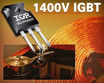
The International Rectifier IRG7PK35UD1 IGBT is optimized for home-appliance applications and is housed in a standard through-hole TO-247 package to keep costs down and simplify installation use on PC boards.

In addition to the 1400-V rating, this IGBT supports 40A continuous collector current and switching speeds from 8 to 30kHz, which is very fast for an IGBT. Due to the voltage, current, and maximum dissipation rating of 167W, it is housed in an industry-standard TO-247 package. The width of each of the three package leads is a little over 1 mm while the minimum lead separation is about 5 mm, commensurate with the 1400V/40A rating (Fig. 5).

TO-247 dimensional drawing

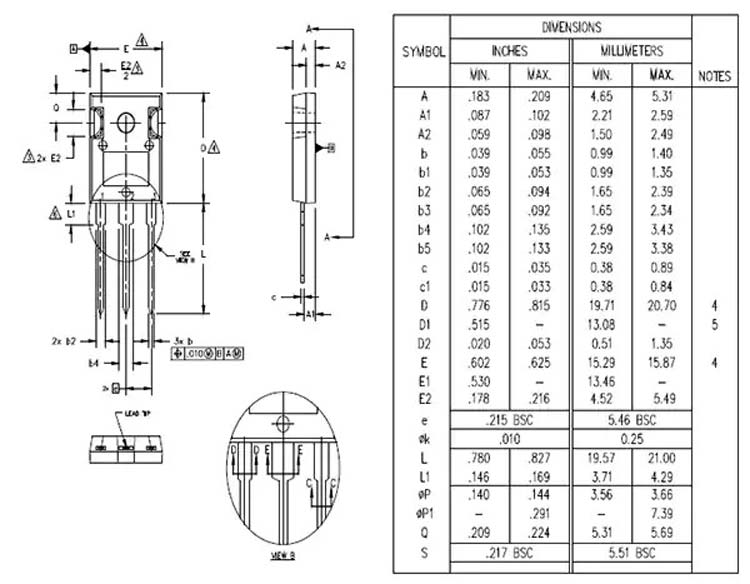
The TO-247 dimensional drawing shows how it must adhere to creepage and clearance mandates for the rated IGBT voltages while handling double-digit currents. (Source: International Rectifier)

The choice of high-voltage IGBT versus MOSFET for applications where they are both viable candidates now has an added dimension: the commercial availability of MOSFETs based on silicon carbide (SiC) rather than traditional silicon alone. In a SiC device, the wider band-gap and other detailed physics result in breakdown voltages that can be 10 times higher than for silicon. The result is that it is possible to fabricate SiC MOSFETs that are much thinner and smaller, and capable of carrying more current with fewer losses, despite other limitations within the SiC device. Further, SiC has a much higher thermal conductivity compared to silicon, resulting in superior power densities. For the critical maximum operating temperature parameter, SiC devices can run at a junction temperature of more than 150°C, reducing system-level heat sink and packaging costs.

Cree offers the C2M family of 1220V and 1700V SiC MOSFETs, also in TO-247 packages, which illustrate this shift. The C2M0160120D is rated to 1.2kV at 17.7A, with just 160mΩ RDS(on), and has a 125W power-dissipation rating; their C2M0160120D is also a 1.2kV device, but for currents up to 90A, with just 25mΩ RDS(on), and a maximum dissipation rating of 463W. This family is well-suited for solar inverters, high-voltage DC/DC converters, motor drives, switch-mode power supply (SMPS), and uninterruptible power-supply (UPS) designs. Cree claims that their SiC MOSFETS have three times the power density of silicon-based IGBTs, and just 20 percent of the losses- both very significant improvements (Fig. 6).

MOSFETs and IGBTs graph

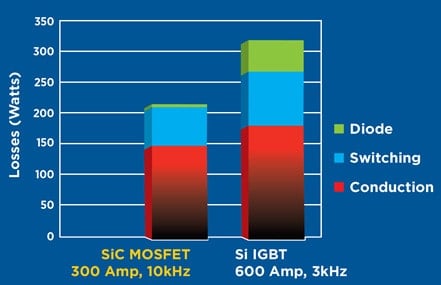
MOSFETS based on silicon carbide offer substantially better high-voltage/high-current efficiency and density than roughly comparable silicon MOSFETs and IGBTs; 300A SiC is more capable than 600A IGBTs (Shown: 250A RMS @ 500V; Source: Cree)

Despite the many challenges of design directly with -- or even just around -- these high voltages, they are an unavoidable, essential aspect of many products. That's why it is important for engineers to be familiar with the associated design aspects and basic high-voltage-related issues, as well as safety and regulatory concerns, to develop a proper perspective along with respect for what high voltages can do and why they are needed.

About Author

Bill Schweber is an electronics engineer who has written three textbooks on electronic communications systems, as well as hundreds of technical articles, opinion columns, and product features. In past roles, he worked as a technical web-site manager for multiple topic-specific sites for EE Times, as well as both the Executive Editor and Analog Editor at EDN. He has been on both sides of the technical PR function, presenting company products, stories, and messages to the media and also as the recipient of these.

He has an MSEE (Univ. of Mass) and BSEE (Columbia Univ.), is a Registered Professional Engineer, and holds an Advanced Class amateur radio license. Bill has also planned, written, and presented on-line courses on a variety of engineering topics, including MOSFET basics, ADC selection, and driving LEDs.

Original source: Mouser

Have any question realated to this Article?

Ask Our Community Members

AMO Electric Bikes Intends to Concentrate on AI and IoT Technologies in the Future

In addition to creating an economic boost, it was always expected that this astoundingly revolutionary approach to transportation electric mobility would provide a significant amount of employment, which would be necessary to overhaul the conventional auto industry, which is still dependent on the unsustainable burning of petrol and diesel.

Rajiv K Vij, Founder of Plug Mobility explains how EV firms are Lowering Carbon Footprint in India

There are no toxic emissions from the tailpipe of electric cars, but the electricity generation while charging the cars might discharge carbon pollution. The volume depends on how the local power is sourced, that is utilizing natural gas or coal that are responsible for carbon pollution, while renewable sources like solar or wind do not emit toxic gasses.

Amid Tough Challenges Why International Wafer Fab Equipment Market to Grow in 2022?

Back in 2019, before the pandemic, the semiconductor equipment industry suddenly faced a huge slowdown coupled with severe technical impediments, which are still looking for an accurate solution. In 2017, the same equipment sector witnessed a colossal demand and the same has been extended into Q1 of 2018. But, interestingly, in the middle of 2018, the memory market started decaying, which in the end forced the vendors of DRAM and NAND to extend or rather reject their equipment orders. Experts on the other hand already predicted that the momentum of this downturn will be carried out throughout 2019 and will hamper the equipment manufacturers with exposure of NAND and DRAM. After that, geopolitical tension appears, and the business tussle between China and the US is a matter of serious concern even though the indelible collision remains unclear.

But, before proceeding further we must understand what the semiconductor equipment is all about. In the fab, there is an imperative process, which is IC manufacturing and there the semiconductor equipment plays an important role. Then, the semiconductor wafer fabrication is utilized to craft circuits that are further utilized in electrical and electronic products. Now, during semiconductor device fabrication, a vast range of procedures are utilized to alter a bare silicon wafer into a circuit. The different procedures comprise CMP (chemical-mechanical planarization), PVD/CVD (physical or chemical vapor deposition), and  RTP (rapid thermal processing) plasma etch, photolithography.

The semiconductor wafer fabrication entails important steps of the photolithographic and chemical process that makes a semiconductor product. On the other hand, the device fabrication requires four steps that comprise different procedures ranging from removal to modification of electrical properties, and deposition. When the fabrication process is completed, silicons are used to manufacture the wafers. Silicons are cooled, melted, and purified to shape an ‘ingot’ that is then cut into wafers. In order to assure the state-of-the-art quality of the semiconductor equipment, a wafer test is performed to supervise the damages because it aids in monitoring whether the processing can be completed or not.

Now, the question is why the demand of this market is augmenting. Various characteristics such as the escalating demand from the consumer and B2B electronics industry coupled with ever-increasing technological improvements in the semiconductor and telecom industry are speculated to spearhead the demand for the semiconductor wafer fab equipment market from 2019-2030. There are some additional factors like equipment and silicon wafer that would assist in analyzing the concerned market in the coming years. Most importantly, new-fangled innovation in wafer technology has crafted a denser packaging of devices like transistors and MEMS (micro-electro-mechanical system) are speculated to create a way for the foundation of innovative opportunities that can be leveraged by various global firms.

The New Road of Problems for the Semiconductor Equipment Sector

Counting the massive demand for memory, the semiconductor equipment sector was anticipated to grow by 15.5 percent back in 2018 as noted by VLSI Research. But, as the memory market at that time witnessed a downturn it was speculated to pull down the entire industry, which in the end caused a decrease in the IC market by 1.6 percent in 2019. On the other hand, the semiconductor equipment industry is following the same path. According to the experts, 2018 was a massive year for the semiconductor industry’s growth, but the memory market’s reduction in demand reduced the pace of the semiconductor industry. Both the semiconductor and memory market was speculated to gain back the pace, but somehow, the downturn that was carried out in the Q2 of 2018 was witnessed during the entire 2019, a year before the pandemic surfaced. 2019 was expected to be optimistic, but sadly both the markets declined in 2019 and the effect was felt till now after the pandemic. This is because there is some sort of over-build in the sectors discussed above and more uncertainty was added when entire China was under stern lockdown. Calculating the entire problem is the memory decline. In 2019, the sales declined to almost 10 percent where it was expected the market to be positive with a growth rate of 4 percent.

However, it has broken the entire semiconductor equipment market. In another survey, the US-based industry association SEMI stated that the international sales of top-notch semiconductor equipment would escalate from 9.7 percent to $62.1 billion in 2018, but in 2019, the market reduced by 4 percent. In the same year, South Korea turned to be the biggest supplier of semiconductor equipment, which is then followed by Taiwan and China, claims SEMI. The picture is also hazy from the applications perspective because the smartphone market remained dull at that time, but additional applications like wireless, automotive, and AI were expected to lead the IC demand.

Wafer Fab Equipment Market

In order to grab the vein of the market to carefully examine the demand picture of two key important centers in the IC sector-photomasks and silicon wafers. SEMI clearly noted that the shipments of silicon wafers were 13,090 million square inches in 2019, which is about 5.2 percent more than 2018. The shipment was about 7.1 percent during 2018. In 2019, the photomask market outstripped to $billion, which is more than 4 percent in 2018.

For several years, China has been a huge prospective market for semiconductor equipment, but nonetheless, trade scuffles are posing a huge problem in this region. In this country, there are two varieties of chip manufacturers; domestic and international firms. Domestic firms have been investing for many years to perk up the industry. An unnamed industry expert stated that 200mm is a very imperative equipment market and the demand for RF chips, analog, and MEMs caused the scarcity of 200mm fab equipment and capacity.

The Sudden Growth of Wafer Fab Equipment Market

According to the experts at Counterpoint Research, the paucity of semiconductors is going to pose a huge challenge to the Wafer Fab Equipment supply chain this year. But, interestingly the profits of the WFE manufacturers are speculated to augment 18 percent this year, which will surpass the $129 billion market. This investment in this sector will grow this year due to the massive spending on higher semiconductor performance, complex technology transformations, ongoing investments for the expansion of production capacity, and escalating manufacturing and device intricacy.

The WFE market looks very promising because foundries are undertaking tough efforts to enhance wafer output, ameliorate productivity and decrease defects. On the other hand, the demand is now exceeding supply and in fact, the wafer processing steps are escalated to offer intricate and manifold applications. In 2021, the investments in WFE are restricted by supply, and the demands that are unmet are pushed to 2022 and moreover, customers have extended the allocations of capex.

Wafer Fab Equipment Manufacturer

Highlighting the reason behind the growth of the WFE market, senior research analyst, Ashwath Rao told, “This year, the top five WFE manufacturer's revenue will surpass $100 billion, which is due to the increasing capital volume, new-fangled product range, sturdy demand of chips across various industries, and well-built WFE investment outlook. As the global supply chain has been hampered, there is not much availability of components for WFE sub-systems, which would augment the lead time of equipment and obstruction of deliveries. This will lead to the fall of revenue during the Q1.”

If the market of WFE is carefully examined, it will reveal that towards the end of 2021, the revenue recorded a staggering growth of $110 billion, an escalation of 33 percent YoY, spearheaded by the sturdiness of varied segments such as Foundry/Logic, NAND, DRAM. The top five supplier’s service revenue recorded 29 percent YoY to $22.2 billion. The year back in 2020, the overall growth of various segments across the market was escorted by Foundry/Logic enhancement, NAND recovery, and a bit of increase in the market for DRAM assisted in grabbing the total revenue growth of $83 billion, an extension of 17 percent YoY.

“In spite of supply chain obstructions due to the pandemic and increased geopolitical problems, during the Q2 of 2022, moderate growth of WFE industry will be witnessed. Along with that, gross for that year will also be reduced due to the impact of price increases due to workforce, logistics prices, and components from suppliers. The new drift towards export regulations between regions also entails close supervision. Hence, growth in Q2 is speculated to be dampened,” added Rao.

Have any question realated to this Article?

Ask Our Community Members

How to Select the Best GSM/GPS Module for a Vehicle or Asset Tracking Applications

When starting a project, the first challenge is to select the best parts for it. In the case of a tracking project, the main parts would be the GPS and GSM modules are the main components. This article will help you find the best ones from the choices available in the market. We will discuss the features or specifications you should check before sourcing these parts.

Things to Consider before Purchasing a GPS Module

  • Size: Sizing matters as it may affect not only the size constraints but also other technical parameters like lock time and accuracy etc. For applications like tracking, we will need the module with the smallest size possible without any compromise in the accuracy or the response time, etc.
  • Update Rate: The update rate of a GPS or GNSS module is basically how often it recalculates and reports its position. The standard for most devices is 1Hz (Only once per second). 5-10Hz update rates can be considered if you need them to work on faster vehicles which are not required in most real-life scenarios.
  • Communication Interface: It’s the interface used to communicate with the GPS Module. Serial/TTL or the USB interface is the most commonly used interface type by the GPS module.
  • Communication Speed/Baud Rate Refers to the speed of communication between the microcontroller and the GPS module, in the case of serial interface it is called the baud rate. Higher the baud rate allows for faster GPS data to be sent to the MCU.
  • Navigation Sensitivity dBm figure dictates how prone the GPS module is able to capture the signal from the satellites. Higher dBm indicates that the module is able to better pick up satellite signals
  • Power Requirements include the working voltage and the power consumption. It is necessary to select the proper device because in most cases the modules will be battery powered and we will need to conserve the battery to maximize working time. The average power consumption of most common GPS modules is around 30mA at 3.3V
  • Number of Channels that the GPS module runs will affect your time to first fix (TTFF). Since the module doesn’t know which satellites are in view, the more frequencies/channels it can check at once, the faster a fix will be found. After the module gets a lock or fix, some modules will shut down the extra blocks of channels to save power. If you don’t mind waiting a little longer for a lock, 12 or 14 channels will work just fine for tracking.
  • Accuracy: Lower the distance it can get down to = Higher accuracy. Usually able to find out your location within 30 seconds, down to +/- 10m. Most modules can get it down to +/-3m
  • Antenna: Remember, that little GPS module is receiving signals from satellites about 12,000 miles away in the sky. For the best performance, you want a clear path between the antenna and most of the sky. Weather, clouds, and snowstorms shouldn't affect the signal, but things like trees, buildings, mountains, and the roof over your head, will all create unwanted interference, and your GPS accuracy will suffer. So, the choice of the proper antenna is very crucial.
  • Gain: The gain is the efficiency of the antenna in any given orientation. This applies to both transmitting antennas and receiving antennas.
  • Chipset: The GPS chipset is responsible for doing everything from performing calculations, to providing the analog circuitry for the antenna, to power control, to the user interface. It’s a lot of work, and yet that’s exactly what these tiny GPS units are doing. The chipset is independent of the antenna type, therefore you can have a range of different antennas for GPS modules with specific chipsets. Common chipsets are ublox, SiRF, and SkyTraq, and all contain very powerful processors that allow for fast acquisition times and high reliability. The differences between chipsets usually fall on a balance between power consumption, acquisition times, and accessibility of hardware. So, choosing the best one for our application is a crucial part.
  • Price: Last but not least the price of the module is very important. It is very important to keep everything under the budget.
  • Time to First Fix(TTFF): Time taken for satellite lock after power-up or reboot.

So now as we know what we are looking for in a GPS Module, let us take a look at a few GPS Modules in the market now:

NEO-6M GPS Module

NEO-6M GPS Module

Considered as one of the more popular GPS modules in the market, the NEO-6M module is a family of stand-alone GPS receivers from the NEO-6 module series.

Based on the list of considerations:

Size: 23mm x 30mm

Update Rate: 1 Hz, 5Hz maximum

Power Requirements:

  • Power Supply Voltage: 3V – 5V

Baud Rate: 9600

Communication Interface: UART

Sensitivity: -161dBm

Number of Channels: 50

Time to First Fix:

  • Cold Start: 27s
  • Warm Start: 27s
  • Hot Start: 1s
  • Aided Starts: <3s

Antennas: Includes external patch antenna

Accuracy:

  • 2.5m GPS Horizontal Position Accuracy

Product Applications:

  • Battery-operated mobile devices
  • GPS tracker
  • GPS navigator

NEO-M8N GPS Module

NEO-M8N GPS Module

The NEO-M8M GPS Module with Ceramic Active Antenna series of concurrent GNSS modules is built on the high-performing M8 GNSS engine in the industry-proven NEO form factor. The NEO-M8M is optimized for cost-sensitive applications, while NEO-M8N/M8Q provides the best performance and easier RF integration. The NEO-M8N offers high performance also at low power consumption levels. The future-proof NEO-M8N includes an internal Flash that allows future firmware updates. This makes NEO-M8N perfectly suited to industrial and automotive applications.

Based on the list of considerations:

Size: 23mm x 30mm

Update Rate: 1 Hz, 5Hz maximum

Power Requirements:

  • Power Supply Voltage: 3.6V

Baud Rate: 9600

Communication Interface: UART/USB/SPI

Sensitivity: -164dBm

Number of Channels: 72

Time to First Fix:

  • Cold Start: 26s
  • Hot Start: 1s
  • Aided Starts: 4s

Antennas: Includes external patch antenna

Accuracy:

  • 2.5m GPS Horizontal Position Accuracy

Product Applications:

  • Battery-operated mobile devices
  • GPS tracker
  • GPS navigator

SIM28ML

SIM28ML Module

SIM28ML is a small, high-performance, and reliable GPS module. This is a standalone L1 frequency GPS module in an SMT type and it is designed with an MTK high sensitivity navigation engine, which allows you to achieve the industry’s highest levels of sensitivity, accuracy, and Time-to-First-Fix (TTFF) with the lowest power consumption.

Size: 10.1*9.7*2.5mm

Update Rate: Up to 10Hz, 1Hz by default

Power Requirements:

  • Power Supply Voltage: 2.8~4.3V
  • Power consumption
    • Acquisition 17mA
    • Tracking 16mA
    • Backup 8uA

Baud Rate: Adjustable 4800bps~115200bps Default: 9600bps

Communication Interface: UART

Sensitivity: -165dBm

Number of Channels: 22 (Tracking)/ 66 (Acquisition)

Time to First Fix:

  • Cold Start: 32s
  • Warm Start: 3s
  • Hot Start: <1s

Antennas: Embedded patch antenna: 15.0mm × 15.0mm × 4.0mm

Accuracy:

  • 2.5m GPS Horizontal Position Accuracy

Product Applications:

  • Battery-operated mobile devices
  • GPS tracker
  • GPS navigator

Quectel L80

Quectel L80 Module

L80 GPS module with an embedded patch antenna and LNA brings the high performance of MTK positioning engine to industrial applications. It is able to achieve the industry’s highest level of sensitivity, accuracy and TTFF with the lowest power consumption in a small-footprint leadless package. With 66 search channels and 22 simultaneous tracking channels, it acquires and tracks satellites in the shortest time even at the indoor signal level. The embedded flash memory provides the capacity for users to store some useful navigation data and allows for future updates.

Size: 16.0mm × 16.0mm × 6.45mm

Update Rate: Up to 10Hz, 1Hz by default

Power Requirements:

  • Power Supply Voltage: 3.0V~4.3V Typical voltage: 3.3V

Baud Rate: Adjustable 4800bps~115200bps Default: 9600bps

Communication Interface: UART

Sensitivity: -165dBm

Number of Channels: 22 (Tracking)/ 66 (Acquisition)

Time to First Fix:

  • Cold Start: 35s
  • Warm Start: 30s
  • Hot Start: 1s

Antennas: Embedded patch antenna: 15.0mm × 15.0mm × 4.0mm

Accuracy:

  • 2.5m GPS Horizontal Position Accuracy

Product Applications:

  • Battery-operated mobile devices
  • GPS tracker
  • GPS navigator

Beitian BN-220

Beitian BN-220 Module

BN-220 is a small gps receiver module, with 4M flash to save the configuration. It is mostly used with drones.

Size: 16.0mm × 16.0mm × 6.45mm

Update Rate: 1Hz-10Hz,Default1Hz

Power Requirements:

  • Power Supply Voltage: 3.0V~5.5V Typical voltage: 5V

Baud Rate: Adjustable 4800bps~921600bps Default: 9600bps

Communication Interface: UART

Interface Protocol: NMEA-0183orUBX,DefaultNMEA-0183

Sensitivity: -167dBm

Number of Channels: 72Channel(Acquisition)

Time to First Fix:

  • Cold Start: 26s
  • Warm Start: 25s
  • Hot Start: 1s

Antennas: Embedded patch antenna

Accuracy:

  • 2m GPS Horizontal Position Accuracy

Product Applications:

  • Drones

Grove – GPS Module

Grove – GPS Module

The Grove – GPS Module is the Seeed version of a GPS receiver that’s cost-efficient and field-programmable. It’s armed with a SIM28 and serial communication configuration.

Size: 40mm x 20mm x 13mm

Update Rate: 1 Hz, max 10 Hz

Power Requirements: 3.3/5V

Baud Rate: 9600 – 115,200

Communication Interface: UART

Sensitivity: -160dBm

Number of Channels: 22 tracking/66 acquisition channels

Time to First Fix:

  • Cold starts with EASY: 13s
  • Warm Starts with EASY: 1-2s
  • Hot Starts: <1s

*EASY is a self-generate orbit protection

Antennas: Antenna included in the package

Accuracy: 2.5m GPS Horizontal Position Accuracy

Product Applications:

  • GPS tracker
  • GPS navigation
  • Distance measurement

Other Product Features:

  • Low power consumption
  • Baud rates configurable
  • Grove compatible interface

Grove – GPS (Air530)

Grove GPS Air530

Next up, we have the Grove – GPS (Air530). It’s a high-performance, highly integrated multi-mode satellite positioning and navigation module. It supports GPS / Beidou / Glonass / Galileo / QZSS / SBAS, which makes it suitable for GNSS positioning applications such as car navigation, smart wear, and drone.

If your GPS isn’t working well in urban areas or outdoors under only one or a few satellite modules, you should definitely check out this GPS module. Meanwhile, this module is capable of receiving more than 6 satellites at the same time and is able to work excellently even if there’s a very bad signal.

This GPS adopts the integrated design of RF baseband, which integrates DC/DC, LDO, LNA, RF front-end, baseband processing, 32-bit RISC based chip, RAM, FLASH storage, RTC and power management functions.

Size: 40mm x 20mm x 13mm

Update Rate:

Power Requirements: 3.3/5V

Baud Rate: – 9600 –921600

Communication Interface: UART

Sensitivity: – –166dBm

Number of Channels:

Time to First Fix:

  • Cold start: 30 seconds
  • Warm Start: 4 seconds

Antennas: Antenna included in the package

Accuracy: 2.5m Horizontal positioning accuracy

Product Applications:

  • GPS tracker
  • GPS navigation
  • Distance measurement

Other Product Features:

  • Highly integrated Multi-mode satellite positioning and navigation
  • Grove compatible interface

Things to Consider before Purchasing a GSM Module

  • Size: Similar to the GPS module the size matters in the case of a GSM module too. The smaller the size more compact our project will be.
  • Communication Interface: It’s the interface used to communicate with the GSM Module. Serial/TTL or the USB interface is the most commonly used interface type by the GSM module.
  • Communication Protocol: Communication protocol is used to communicate with the module. Most modules use AT Commands for this purpose. With AT commands, there will be commands to control each function of the module. We will use these commands to configure the module, to get information from the module, for services SMS, MMS and for voice and data links too.
  • Communication Speed /Baud rate Refers to the speed of communication between the microcontroller and the GSM module, in the case of serial interface it is called the baud rate. Higher the baud rate allows for faster GSM data to be sent to the MCU.
  • Communication Standard refers to the mobile standards like GSM, CDMA, WCDMA, LTE etc. GSM commonly stands for 2G, WCDMA for 3G and LTE for 4G communications. And the CDMA is no longer used in most areas of the world.
  • Supported Frequency Bands refers to the frequency bands supported by the module. 900MHz and 1800Mhz are the most common 2G bands in India while 900MHz and 2100MHz are the 3G bands. And for 4G the most common bands used in India are  B1 (2100 MHz), B3 (1800 MHz), B5 (850 MHz), B8 (900 MHz), B40 (TDD 2300 MHz), B41 (TDD 2500 MHz). So it is very important to choose the correct module which supports the bands supported by the carrier in the intended area.
  • Supported services refers to the services supported by the module including voice, SMS and data. Some even support FM. Not all modules support all the protocols. So be careful when choosing the correct one.
  • Data Transmission Throughout It refers to the maximum upload and download data speed supported by the module. For example, the most famous SIM800L has a maximum upload and download speed of 85.6kbps, while the SIM7500 module supports up to 150Mbps of download and 150Mbps of upload speed in LTE Category 4. So, if our applications need more bandwidth we must choose accordingly.
  • Transmit Power: Transmission power of the module. Higher the power higher the reception, but with higher power usage. Not only that the power regulation may vary with countries so make sure to choose the correct module with proper transmission power rating as per your regulatory authorities.
  • Power Requirements: This includes the working voltage and the power consumption. It is necessary to select the proper device because in most cases we will the modules will be battery powered and we will need to conserve the battery to the maximum.
  • Price: Last but not least the price of the module is very important. It is very important to keep everything under the budget.

So now as we know what we are looking for in a GSM Module, let us take a look at a few GSM Modules in the market now:

SIMCOM SIM800L

SIMCOM SIM800L

SIM800L is a quad-band GSM/GPRS module, that works on frequencies GSM850MHz, EGSM900MHz, DCS1800MHz and PCS1900MHz. SIM800L features GPRS multi-slot class 12/ class 10 (optional) and supports the GPRS coding schemes CS-1, CS-2, CS-3 and CS-4. With a tiny configuration of 15.8*17.8*2.4mm, SIM800L can meet almost all the space requirements in user applications, such as smartphones, PDA and other mobile devices. SIM800L has 88pin pads of LGA package and provides all hardware interfaces between the module and customers’ boards.

SIM800L GSM Module

It is also available as a module. The image of the module is given above.

Size:  15.8*17.8*2.4mm

Communication Interface:  UART/USB

Communication Protocol: AT Command

Communication Speed /Baud rate: 1200bps to 115200bps

Communication Standard: GSM GPRS(2G)

Supported Frequency Bands: Quad-band: GSM 850, EGSM 900, DCS 1800, PCS 1900

Supported services: Voice, SMS, DATA GPRS

Data Transmission Throughout: GPRS data downlink transfer: max. 85.6 kbps/GPRS data uplink transfer: max. 85.6 kbps 

Transmit Power: Class 4 (2W) at GSM 850 and EGSM 900, Class 1 (1W) at DCS 1800 and PCS 1900

Power Supply: 3.4V ~4.4V typical power consumption in sleep mode is 0.7mA

Ai Thinker A9 GPRS Series Module

​Ai Thinker A9 GPRS Series Module

Ai Thinker A9 GPRS Series Module can be used in a wide range of IoT applications and is ideal for IoT applications for home automation, industrial wireless control, wearable electronics, wireless location sensing devices, wireless location system signals, and other IoT applications. The A9 is a complete quad-band GSM / GPRS module in a compact design SMD package. Its stable performance, appearance of compact, and cost-effective, could meet the diverse needs of customers.

Size: 19.2*18.8*2.7mm

Communication Interface: UART/USB/I2C

Communication Protocol: AT Command

Communication Speed /Baud rate: 1200bps to 115200bps

Communication Standard: GSM GPRS(2G)

Supported Frequency Bands: 850, 900, 1800, 1900MHZ

Supported services: Voice, SMS, DATA GPRS

Data Transmission Throughout: GPRS data downlink transfer: max. 85.6 kbps/GPRS data uplink transfer: max. 42.8Kbps

Transmit Power: Class 4 (2W) at GSM 850 and EGSM 900, Class 1 (1W) at DCS 1800 and PCS 1900

Power Supply: 3.8V-4.2V, 4V power supply is recommended

IoT-GA6 Mini GPRS GSM Module

IoT-GA6 Mini GPRS GSM Module

GA6 module is a mini version of serial GSM / GPRS core development board based on GPRS A6 chip. This chip supports GSM/GPRS network, available for GPRS and SMS message data remote transmission. With the help of the A6 chip, GPRS never deactivated until its application is on and online. It supports either digital and analog audio, with HR, FR, EFR, AMR voice coding. This module can add voice, text, SMS, and data capabilities to your Arduino project. It has more price to performance value than the SIM800, SIM900 modules. This small and low power consumption module can communicate with the microcontrollers and Arduino boards through the UART interface, with the capability of command reception, including GSM 07.07, GSM 07.05 standards. It can be used for IoT projects, M2M applications, industrial automation, BMS projects, home automation, public transportation, personal tracking, electricity environment detection, wireless POS, smart metering, and other M2M applications

Size: 17.6*15.7*2.3mm

Communication Interface: UART/USB

Communication Protocol: AT Command

Communication Speed /Baud rate: 115200bps

Communication Standard: GSM GPRS(2G)

Supported Frequency Bands: Quad-band: GSM 850, EGSM 900, DCS 1800, PCS 1900

Supported services: Voice, SMS, DATA GPRS

Data Transmission Throughout: GPRS data downlink transfer: max. 85.6 kbps/GPRS data uplink transfer: max. 42.8kbps 

Transmit Power: Class 4 (2W) at GSM 850 and EGSM 900, Class 1 (1W) at DCS 1800 and PCS 1900

Power Supply: 3.5V ~ 4.2V 3.3V Logic

Quectel M66

Quectel M66 GSM Module

The M66 is a quad-band GSM/GPRS 2G module measuring 17.7mm × 15.8mm × 2.3mm which uses LCC castellation packaging. Based on the latest 2G chipset, it is optimized for data, SMS and audio transmission, and is designed for low-power IoT use cases that operate in harsh conditions. The M66 uses surface-mounted technology, making it ideal for large-scale manufacturing, which can have strict requirements on cost and efficiency. The M66’s ultra-compact profile makes it particularly suited to size-sensitive applications, and the module can serve a range of applications such as wearable devices, automotive, PDAs, asset tracking, POS, smart metering and telematics.

Size: 17.7mm × 15.8mm × 2.3mm

Communication Interface: UART/USB

Communication Protocol: AT Command

Communication Speed /Baud rate: 115200bps

Communication Standard: GSM GPRS(2G), Bluetooth 3.0

Supported Frequency Bands: Quad-band: GSM 850, EGSM 900, DCS 1800, PCS 1900

Supported services: Voice, SMS, DATA GPRS

Data Transmission Throughout: GPRS data downlink transfer: max. 85.6kbps/GPRS data uplink transfer: max. 85.6kbps 

Transmit Power: Class 4 (2W) at GSM 850 and EGSM 900, Class 1 (1W) at DCS 1800 and PCS 1900

Power Supply: 3.3V ~ 4.6V

SIMCOM SIM868

SIMCOM SIM868 Module

SIM868 module is the complete Quad-Band GSM/GPRS module which combines GNSS( GPS/GLONASS/BDS) technology for satellite navigation. It has strong extension capability with abundant interfaces including UART, USB2.0, GPIO etc. The module provides much flexibility and ease of integration for customers’ applications.

Size: 17.6*15.7*2.3mm

Communication Interface: UART/USB

Communication Protocol: AT Command

Communication Speed /Baud rate: 1200bps to 115200bps

Communication Standard: GSM GPRS(2G)

Supported Frequency Bands: Quad-band: GSM 850, EGSM 900, DCS 1800, PCS 1900

Supported services: Voice, SMS, DATA GPRS

Data Transmission Throughout: GPRS data downlink transfer: max. 85.6 kbps/GPRS data uplink transfer: max. 85.6 kbps 

Transmit Power: Class 4 (2W) at GSM 850 and EGSM 900, Class 1 (1W) at DCS 1800 and PCS 1900

Power Supply: 3.4V ~ 4.4V

Update Rate: Up to 10Hz, 1Hz by default

Power Requirements:

  • Power Supply Voltage: 3.0V~4.3V Typical voltage: 3.3VCommunication Interface: UART

Sensitivity: -167dBm

Number of Channels: 33 tracking /99 acquisition

Time to First Fix:

  • Cold Start: 28s
  • Warm Start: 22s
  • Hot Start: 1s

Antennas: External

Accuracy:

  • 2.5m GPS Horizontal Position Accuracy

Conclusion

We are concluding this article hoping you got a better idea about the available option for a GPS/GSM module. In the article, we haven’t included any 3G/4G modules since they are not good for such an application, and they are very costly at this point. 2G GSM modules will give the best result because of their coverage and they are dirt cheap nowadays. And modules we have covered are the most common available once in the market and many other variants are there too. You may extend your scope to them if you can’t find a suitable one from the above suggestions.

Have any question realated to this Article?

Ask Our Community Members

DC to DC Converter with Constant Current (CC) and Constant Voltage (CV) Control - Schematics, PCB, Parts List, and Working

In this article we will be learning about the features and working of the XL4015 which is a 5A 180KHz 36V Buck DC to DC Converter. Here we will desolder all the components from the module, completely reverse engineer the schematic and make the PCB from it, so that we can order the components and make the PCB ourselves. In addition, we'll test the module and compare all the datasheet parameters to see if they hold true or not. So without further ado let's get right into it.

XL4015 DC-DC Buck Converter Module Features

A Constant Current (CC), and Constant Voltage (CV) converter can come in very handy in various conditions, for example, if you want to charge a lithium battery with a constant current you can do that very easily with this module. Furthermore, if you are testing a circuit and powering it for the first time it's always recommended to use a constant current that will limit damage to your circuit if you made any mistakes in the build process.

XL4015 DC DC Buck Converter Module

In the above image you can see first we have the DC input connector, which is to connect to an unregulated power source. Next, we have two 10K potentiometers that are used to set the constant current and voltage level. Furthermore, there are three LED indicators on the board; the first one near the input connector shows when the module is in constant current mode, while the other two near the output are mainly for battery charging applications (battery charging and battery full indicators). Other than that, this IC has an input voltage range of 8V to 36V, and the output voltage of the device is 1.25V to 32V. With max load, the PWM of the device can reach 100% duty cycle and it can operate on a 180 kHz operating frequency. The constant output current of the module is 5A and it can reach up to 96% efficiency while working. If we are talking about protection features it has thermal shutdown, short circuit protection, and current limit functionality.

Components used in DC-DC Buck Converter

Before we look at the schematic, here is a list of components that are required to build the XL4015 Buck Converter Circuit. The main component in this board is the XL4015 buck converter IC, that is a 5pin IC designed and developed by XLSEMI which is a well-known manufacturer in china and very famous for producing compact buck and boost converter ICs. The list of components required to build the 5A Buck Converter Circuit is shown below-

DC DC Buck Converter Components

  • XL4015 Buck Converter IC - 1
  • 78L05 Voltage Regulator - 1
  • LM358 op-amp - 1
  • SS54 Schottky Diode- 1
  • TL431 Programmable Reference - 1
  • 470uF,35V Capacitor - 2
  • 10uF 0805 Capacitor -2
  • 10K Ten Turns Trim Pot - 2
  • 0.1uF Capacitor - 3
  • 270R Resistor - 1
  • 1K Resistor - 2
  • 2.2K Resistor - 1
  • 10K Resistor -  1
  • 71.5K Resistor - 1
  • 90.9K Resistor - 1
  • LED 0805 - 3
  • Screw Terminal - 2

Circuit Diagram of the XL4015 5A Buck Converter

The Schematic of the Buck converter is shown below. As you can see it's not that difficult to understand and the overall design of the module is indeed a pretty neat and clever piece of work. The schematic diagram of the module is shown below.

XL4015 DC-DC Buck Converter Schematic

The working of the circuit is simple and difficult at the same time. If we check the datasheet of the XL4015 5A buck converter Module, we can see the typical application schematic that is given below.

XL4015 Module Application Schematic

Now compare the above schematic to our schematic, you can see that it's very similar because the schematic for the buck regulator portion stays the same the only additional difference is that it has additional current limiting functionality.

Now let's understand how the current limiting functionality works. In the schematic, you can see we have a 78L05 Voltage Regulator which is an ultra-low-power regulator that is used to convert the input voltage to a constant 5V for the TL431 IC. The TL431 is a reference that is set to a constant current regulator mode with the help of a 71.5K resistor and a potentiometer. This reference is compared to the sense voltage from the output side of the resistor to limit the current. The circuit shown below is the TL431 circuit that is providing a constant current source to the op-amps. 

TL431 Circuit

Next, we have the first op-amp portion; this portion of the circuit is actually used to limit the current. What happens in this portion is that the output sense voltage gets compared with the reference voltage from the TL431 IC. Next what happens is that if the output sense voltage is greater than the reference voltage the output of the op-amp turns high and with the shutdown function of the circuit, the output of the IC turns off.

Buck Converter Schematic

In the above image, I have shown you an application circuit from the datasheet with a practical circuit side by side. So in the practical circuit, the manufacturer uses an LED instead of a diode, this LED not only acts as a reverse current blocking but also lights up when the current limit function is active.

Buck Converter Module Circuit

Next, we have the final portion of the circuit, this portion of the circuit is used to indicate the battery charging and fully charged condition. In this circuit when the battery is fully charged, the output goes low so the charging complete LED turns on, now if a battery is charging, the other LED turns on to indicate the battery is charging.

Recreating the PCB for XL4015 Buck Converter

As we have already made the schematic we thought to recreate the PCB for the buck converter modules and we did just that. The dimension of the PCB is 25mm / 50mm. You can see that from the image below.

XL4015 Buck Converter Module PCB Design

Next, we have used the Manufacturing functionality of eagle to determine the top and bottom portion of the PCB and it looks like something that is shown below.

XL4015 Module PCB

In the above image, the TOP side of the PCB is shown, and the bottom side of the PCB is shown below-

XL4015 Buck Converter PCB

That's all for the PCB part and you can download the Gerber file for the project by clicking the given download link.

Testing the XL4015 DC-DC Buck Converter Module

To start the test, we first connect the buck converter module to the power supply and connect the output to the DC load, and we have set a constant load of 1A to test the circuit.

XL4015 Buck Converter Working

Now as that was working, we set the constant current to 5A as it was advertised in the datasheet.

XL4015 CC CV Module Working

If you consider the size of the module I was very impressed to see that it was able to deliver, a constant current of 5A. I tested this circuit for 5 minutes and it was working absolutely fine.

DIY DC DC Buck Converter Module

Next, we tested this circuit for short circuit conditions. As advertised on the datasheet it has built-in short circuit protection, so we also tested that. And it worked absolutely fine.

Problems Encountered while testing the Buck Converter Circuit

While testing the circuit we encountered a major problem in some of these modules. At the time of writing the article, we had 10 modules in our lab but some of those were working, and some of those were not. This made us very confused.

DC DC Buck Converter Module Problem

But the solution to this problem was very simple: we connected a 1uF capacitor to the PCB and the module worked absolutely well without any issues. Other than that we did not find any problems with the module board.

Conclusion

I tested the module under various input/output voltages and load conditions and evaluated its efficiency, and all the tests went smoothly without any issues. So we can say that the XL4051 is a very cost-efficient and highly effective module for demo projects and battery charging.

Have any question realated to this Article?

Ask Our Community Members

How will 5G Support and Benefit India’s Upcoming Technologies and Applications?

A year back, the government of India has taken an initiative to craft the country into a five trillion dollar economy towards the end of 2025, and one of the key requirements to turn this goal into a reality is revolutionizing the nation’s digital infrastructure. The country has already dug deep into enhancing the digital infrastructure, but experts claim that 5G services will be the key to a successful digital India. The question still remains when will 5G be available in the country in a full-fledged way. To answer this question, the Department of Telecommunications (DoT) recently stated that it will be available in mid or Q4 of 2022. The department also proclaimed that at first the services will be available in 13 cities and then the rest of the country will enjoy the benefits of this service. Ahmedabad, Bengaluru, Chandigarh, Gandhinagar, Gurugram, Hyderabad, Jamnagar, Kolkata, Chennai, Lucknow, Pune, Delhi, and Mumbai are the first 13 cities to enjoy 5G.

5G has ultra-low latency through which it will offer speedier and seamless communication all over the world. This next-generation cellular technology will spearhead and empower modern cutting-edge technologies such as the Internet of Things (IoT), Artificial Intelligence (AI), Augmented Reality (AR), Virtual Reality (VR), and machine-to-machine communications. It will ultimately support a huge range of modern applications and use cases such as self-driving, facial recognition systems, connected devices, chatbots, and many more. In an interaction with the media, Nitin Bansal, managing director of Ericsson India said 5G will boost the economic growth in India and it will assist service providers in monitoring and managing the increasing data requirements of consumers in an efficient manner. The early use-cases for 5G in the country are speculated to be fixed wireless access (FWA) and enhanced mobile broadband (eMBB) that would aid in solving the troubles of limited fixed broadband services and perk up the data experience while on the go.

Now, the question is why India needs 5G badly in 2022. Satyajit Sinha, Senior Analyst at IoT Analytics told CircuitDigest, "The mobile operators will not only be assisted by 5G in monitoring the escalating data requirements of consumers, but also open the gates of revenues for them. 5G is already perking-up various industries in the world via commencing the fourth industrial revolution and by improving the network experience for several businesses and end consumers. In fact, 5G is speculated to spearhead the digital transformation of several sectors like education, energy and utilities, automotive, healthcare, manufacturing, and many more. Towards the end of 2030, the anticipated worth of 5G-enabled digitalization revenues in the country will reach around USD 17 billion.”

5G IoT Applications

Source: Pixabay

How 5G will Lead India’s Digital Transformation by 2025

People in the remote corners of the country enjoyed the benefits of 4G in a better way, but at the same time, we cannot overlook the imperativeness of broadband connectivity for the financial and social enhancement of the nation. The lockdowns have underlined the significance of connectivity in every aspect of our life starting from introducing work from home, the commencement of online trade on a large scale, online education and most importantly, connecting people. The digital India initiative that centers on empowerment depends massively on connectivity and the mobile networks in the country continue to offer its services on that promise.

According to telecom experts, 5G is not only about some giga-bit data speeds. In the beginning, the fuss was about the speed of the 5G deployments, but it is going to transform our life the way we live and play, and work. The fundamental shift from 4G to 5G would be multi-dimensional and the immensity is much bigger than the shift from 3G to 4G. 5G will not only offer a wide range of new-fangled spectrum to be put to use, but it will also become more effective than 4G in the spectrum already in utilization. It can accumulate more data than 4G for the same volume of spectrum.

5G will fetch a huge transformational shift in the teaching domain with remote learning coupled with teaching in the classroom to intelligently escalate the educational efficacies. In India, where 70 percent of people live in rural areas it becomes too difficult to provide top-notch education to everyone manually. Hence, 5G backed by ultra-low latency and higher speed will provide proper education and cater to a wider population. Then, when it comes to smart cities and smart homes, devices furnished with sensors communicating to each other will turn into key equipment. For homes specifically, people might witness cutting-edge AI backed personalization, automated grocery lists, tracking electronic devices, and automated deployment of everyday routines. In terms of smart cities, 5G has the potential to offer smart metering systems and smart electricity grids, safety mechanisms, waste disposal systems, and smart traffic management.

Highlighting the importance of 5G in India’s digital transformation, Lt. Gen Dr. S.P Kochhar, Director General, Cellular Operators Association of India (COAI) said, "With the Prime Minister’s inauguration of the 5G testbeds, the industry is on the pathway towards indigenization of 5G and it opens up opportunities for various other new-age technologies such as big data analytics, artificial intelligence (AI), augmented reality (AR) and virtual reality (VR), etc. which will drive major innovations across industries – Manufacturing, Supply Chain, Healthcare, Transportation and bring us closer towards our vision i.e. Digital India. A couple of impediments like cutting-edge infrastructure and Right of Way (RoW) policies being discussed thoroughly among the regulatory bodies and the unveiling of Gati Shakti Sanchar Portal is yet another promising move for the Indian telecom industry. Industry associations like COAI are working closely with the regulatory bodies and service providers to navigate through the challenges and further amplify the initiatives launched by the Government of India.”

COAI also added that 5G network rollout is expected to add $450 billion to the Indian economy, increasing the pace of development and creating jobs. Prime Minister Narendra Modi recently said that 5G technology will bring positive change in the governance of the country, ease of living, and ease of doing business, especially newer opportunities for the B2B businesses.

Current Role of 5G in Averting Security Risks for IoT Devices

In the coming few years, the volume of IoT connections is expected to augment all over the world, which is about 25.2 billion towards the end of 2025, predicts GSMA Intelligence unit. The report also highlighted that over 3.1 billion out of the 25.2 billion would employ cellular technologies comprising low power wide area Mobile IoT networks. These days, a lot IoT backed devices utilizes wireless technology that comprises of short-range technologies, mostly utilizing unlicensed spectrum such as ZigBee, WiFi, and Z-Wave, and also and wide area cellular technologies, using licensed spectrum, such as LTE, 5G, and GSM. According to experts, cellular technologies that operate under a licensed spectrum offer a huge number of advantages for devices powered by IoT. These are mostly service enablement, sophisticated provisioning, and also device management. Apart from that cellular networks provide a huge international coverage and accurate reliability, performance, and security, which are required by the most promising and in demand IoT applications.

Now, talking from a security perspective, there could be 1.8 billion 5G connections by the end of 2025 as per the GSM association. Back in 2020, the 5G IoT market reached a value of USD 1.5 billion and is speculated to stand USD 40 billion by the end of 2026, at a CAGR of 72.9 percent over the time slot between 2021-2026. When 5G is amalgamated with IoT, it escalates the operational performance of several devices, but at the same time, high-end risks emerge. According to Satyajit Sinha, there is huge difference between deployment of IoT and deployment of 5G, which is regarding the standards that are available in either of these technologies.

5G IoT Module Forecast B2B Market

Basically, the IoT powered devices are still highly unregulated and then follow no generic standards. An IoT device is crafted out of hardware and sensors that further connect a layer of software and the sensors. The software manages the hardware and sensor data and also does the computing. Apart from that, there is a communication interface available that permits connection to the 5G network. Now, crafting a basic security architecture is highly intricate as there are several ways to design, build, and utilize an IoT product.

The current risk assessments and methods are not perfectly designed to get to know about the IoT-based risks in a comprehensible manner. The devices will be on all the time and will be connected to the 5G network and ubiquitous. For instance, if you carefully look at smart home implementation, if there is a voice-enabled device, which is connected to an IoT-powered lock on the door, the person opens the door with his or her voice command. It is not fully secured because a thief who came to know the person has left the home, can come to the door and speak with the same voice command and can open the door. The point is there is absence of authentication at the IoT device. Now, another point to be noted is that 5G will still suffer from the 4G weakness, claims experts. Now, it is not possible to unleash a comprehensive 5G network all at once and in fact, in fewer places 5G is moderately deployed side by side a 4G software components and hardware for a certain time slot. Hence, to have a sturdy IoT security platform or a framework, it requires a multi-layered approach.

Conclusion

5G, after a constant transformation in the last two years, has grown from an emerging idea into a pervasive and important technology for mobile devices. The features of 5G that includes ultra-high density, ultra-high-speed, and ultra-low latency will be inserted into AI via wireless. The AI actions can be completed rapidly through 5G on the terminal side and it also perk-up personalized services, boost customer experience and decrease latency. In fact, 5G will also be benefited from the AI-enabled processing ability.

Highlighting the advantages, Neil Shah, Research Vice President at Counterpoint Research said, “The applications that are based on AI can respond in the accurate time to the data generated by the 5G networks, thereby offering new-fangled potentials for automation. Removing the conventional wireless algorithms with the help of proper machine learning, AI will be able to significantly decrease the price of manpower and enhance the total performance. It will also offer safety to the people’s everyday life, encouraging digital transformation, modernizing several commercial and industrial activities, and unleashing endless top-notch products and services.”

Have any question realated to this Article?

Ask Our Community Members

Raspberry Pi Pico Variants – A Detailed Comparison

Raspberry Pi Pico is a low-cost, versatile microcontroller development board from the Raspberry pi foundation. It is constructed around the RP2040 chip, which was designed in-house by the Raspberry Pi Foundation. It was released in January 2021, and it’s been a very popular development board among the DIY community ever since. Now, a year and a half after the first release, the Raspberry Pi foundation just released a few variants for the Pico board namely Pico H, Pico W and Pico WH. Let’s look at all these variants and their differences.

Raspberry Pi Pico – the 4$ ARM Cortex Development Board

Raspberry Pi Pico is the first low-cost Microcontroller development board from the infamous Raspberry Pi Foundation. Available for just $4, the Pico is powered by Raspberry Pi’s own custom silicon RP2040 SoC which features an Arm Cortex M0+ processor running at up to 133 MHz with 264K of SRAM and 2MB of onboard storage. A great choice for any DIY project. Unlike previous boards from the Raspberry Pi foundation, the Pico is not an SBC that can run a full operating system, but a microcontroller development board that can be programmed in MicroPython or C Programming languages.

With a large on-chip memory, symmetric dual-core processor complex, deterministic bus fabric, and rich peripheral set augmented with a unique Programmable I/O (PIO) subsystem, RP2040 provides professional users with unrivalled power and flexibility. With detailed documentation, a polished MicroPython port, and a UF2 bootloader in ROM, it is the best development board for beginner and hobbyist users.

Raspberry Pi Pico

RP2040 is manufactured on a modern 40nm process node by TSMC, delivering high performance, low dynamic power consumption, and low leakage, with a variety of low-power modes to support extended-duration operation on battery power. Raspberry Pi Pico pairs RP2040 with 2MB of Flash memory, and a power supply chip supporting input voltages from 1.8-5.5V. It provides 26 GPIO pins, three of which can function as analogue inputs, on 0.1”-pitch through-hole pads with castellated edges.

Raspberry Pi Pico Board Pinout

Raspberry Pi Pico Pinout

Raspberry Pi Pico Board Specifications

Form factor: 21 mm × 51 mm

CPU: Dual-core Arm Cortex-M0+ @ 133MHz

Memory: 264KB on-chip SRAM; 2MB onboard QSPI Flash

Interfacing: 26 GPIO pins, including 3 analogue inputs

Peripherals:

  • 2 × UART
  • 2 × SPI controllers
  • 2 × I2C controllers
  • 16 × PWM channels
  • 1 × USB 1.1 controller and PHY, with host and

Device Support: 8 × PIO state machines

Input Power: 1.8–5.5V DC

Operating Temperature: -20°C to +85°C

Raspberry Pi Pico H

Raspberry Pi Pico H

Pico H is the same as the original Raspberry Pi Pico. There are no functional differences between them. The main difference is that the old gold-plated castellated holes are removed, and the header pins are pre-soldered.

Raspberry Pi Pico H Board

Another major difference is the new debug connector. The original Pico has a 2.54mm standard header pi for the debug. While the new Pico H has a small, keyed, 3-pin SM03B-SRSS-TB connector which can be used for either UART or 2-wire serial debug interfaces. Everything else including physical dimensions and pinout is the same as the original Pico.

Raspberry Pi Pico W and WH

Even though the Raspberry Pi Pico is a very powerful board, its main disadvantage over its competitors like ESP8266 or ESP32 is the lack of wireless connectivity. The new Pico W and WH have the solution for that. The new Pico W comes with an Infineon CYW43439 chip that’s supposed to support both 2.4 GHz WiFi 4 and Bluetooth LE 5.2. Even though the Chip supports Bluetooth 5.2, it is not enabled at this time. The Raspberry Pi foundation may enable it in the future through some firmware updates.

Raspberry Pi Pico W and WH

The Wi-Fi module and antenna have been added, but other than that, the design is basically the same as the Pico. The user LED is now connected to the CYW43439 wireless chip but is still controllable from the RP2040 SDK. It’s pin-to-pin compatible with the original Raspberry Pi Pico so existing add-ons or carrier boards should work without modifications.

Raspberry Pi Pico W and WH Components

The buck converter on the Pico W is also changed to meet the new power demands. The new Pico W uses the RT6154A from Richtek as the power regulator instead of the RT6150B in the original Pico design. The debug port also moved near the SoC to make space for the Wi-Fi antenna.

Raspberry Pi Pico W and WH Pinout

As you can see there isn’t really much difference between the original Raspberry Pi Pico and the new Pico W. We have the same GPIO, microUSB port, dimensions and SoC. The only difference is the inclusion of Infineon’s CYW43439 2.4-GHz Wi-Fi chip. Just like the Pico H, the Pico WH is the Pico W with already populated header pins and it’s yet to be released. Unfortunately, no reference images are available to make sure of any other changes.

You can also check out Raspberry Pi Pico Projects and Tutorials here.

Have any question realated to this Article?

Ask Our Community Members

The Biggest Challenge for Indian Electronics and Semiconductor Industry is Still Availability of Funds, Investments

In the past few years, India has witnessed an applaudable escalation in in-house production of electronics goods, but in spite of this augmentation, the country is still dependent on imports of electronic components from other countries. It shows that although several advancements are taking place in manufacturing and technology, there are still various challenges that are disturbing the ecosystem.

Anechoic Chamber Used for Electronics Testing

Devoid of electromagnetic waves, an anechoic chamber (Figure 1) is a shielded room designed to provide an ideal environment for testing electronics. Anechoic means free from echoes—or non-reflective. These chambers are used in compliance testing. The surfaces of anechoic chambers are lined with carbon-based absorbing materials (Figure 2) and ferrite tiles in order to eliminate electromagnetic emanation, radiation, and reflection.

Staff Mon, 06/27/2022 - 17:49