
In this article, we will be learning about the features and working of the XL4015, which is a 5A 180KHz 36V Buck DC to DC Converter. Here we will desolder all the components from the module, completely reverse engineer the schematic and make the PCB from it, so that we can order the components and make the PCB ourselves. The XL4015 DC-DC buck converter is a versatile step-down converter that provides both constant current (CC) and constant voltage (CV) regulation. In addition, we'll test the module and compare all the datasheet parameters to see if they hold true or not. So without further ado, let's get right into it. This complete guide will provide you with the DC to DC buck converter circuit diagram outlines, reverse engineering, PCB layout, and practical testing to enable you to understand the dc dc buck converter working principle and build your own module.
XL4015 DC-DC Buck Converter Module - Quick Overview
Build Time: 6-8 hours | Cost: $10-20 | Difficulty: Intermediate
What You'll Learn: PWM switching, Constant Current/Voltage regulation, PCB design, Circuit debugging
Applications: Battery charging, Voltage regulation, LED driving, Power supply prototyping
Table of Contents
Understanding DC-DC Buck Converter Working Principle
The core concept behind a dc dc buck converter working principle is the combination of energy storage in an inductor and switching controls. The XL4015 IC contains an internal MOSFET switch and controls the output voltage using PWM (Pulse Width Modulation) to make the MOSFET switch's duty cycle larger or smaller. When the switch is closed, the inductor will draw a current and store energy. In other terms, during this type of operation, the work done on the inductor is transferred to the output via the freewheeling diode. This switching of the inductor and switch allows continuous energy delivery to the load without any breaks in current.
Some key components are defined during the buck converter operation:
- Switching Element: Internal MOSFET implemented on XL4015
- Energy storage: Inductor (Usually a 68µH Inductor)
- Freewheeling Diode: SS54 Schottky Diode for good efficiency
- Filter Capacitors: Input and Output Smoothing
XL4015 DC to DC Buck Converter Module Features
This DC to DC buck converter module combines a Constant Current (CC) and Constant Voltage (CV) converter, which comes in very handy in various conditions. For example, if you want to charge a lithium battery with a constant current, you can do that very easily with this module. Furthermore, if you are testing a circuit and powering it for the first time, it's always recommended to use a constant current that will limit damage to your circuit if you made any mistakes in the build process.
XL4015 Buck Converter Specifications
| Parameter | Specification |
| Input Voltage Range | 8V to 36V |
| Output Voltage Range | 1.25V to 32V |
| Maximum Output Current | 5A Continuous |
| Switching Frequency | 180 kHz |
| Maximum Efficiency | 96% |
| Operating Mode | CC/CV (Constant Current/Constant Voltage) |
| Protection Features | Thermal shutdown, Short circuit, Current limit |
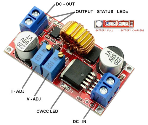
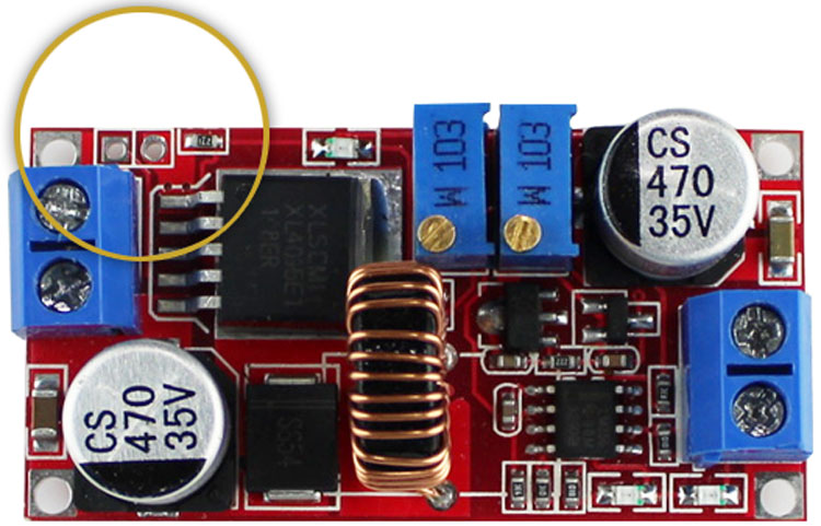
In the above image, you can see first we have the DC input connector, which is to connect to an unregulated power source. Next, we have two 10K potentiometers that are used to set the constant current and voltage level. Furthermore, there are three LED indicators on the board; the first one near the input connector shows when the module is in constant current mode, while the other two near the output are mainly for battery charging applications (battery charging and battery full indicators). Other than that, this IC has an input voltage range of 8V to 36V, and the output voltage of the device is 1.25V to 32V. With max load, the PWM of the device can reach 100% duty cycle, and it can operate on a 180 kHz operating frequency. The constant output current of the module is 5A, and it can reach up to 96% efficiency while working. Regarding protection features, the device includes thermal shutdown, short-circuit protection, and current limit functionality.
Components Used in the DC-DC Buck Converter
Before we look at the schematic, here is a list of components that are required to build the XL4015 Buck Converter Circuit. Building your own DC to DC buck converter module requires specific components. The main component in this board is the XL4015 buck converter IC, which is a 5-pin IC designed and developed by XLSEMI which is a well-known manufacturer in China and very famous for producing compact buck and boost converter ICs. The list of components required to build the 5A Buck Converter Circuit is shown below-
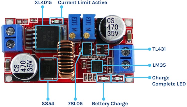
- XL4015 Buck Converter IC - 1
- 78L05 Voltage Regulator - 1
- LM358 op-amp - 1
- SS54 Schottky Diode- 1
- TL431 Programmable Reference - 1
- 470uF,35V Capacitor - 2
- 10uF 0805 Capacitor -2
- 10K Ten Turns Trim Pot - 2
- 0.1uF Capacitor - 3
- 270R Resistor - 1
- 1K Resistor - 2
- 2.2K Resistor - 1
- 10K Resistor - 1
- 71.5K Resistor - 1
- 90.9K Resistor - 1
- LED 0805 - 3
- Screw Terminal - 2
Complete DC to DC Buck Converter Circuit Diagram Analysis
The Schematic of the XL4015 buck converter circuit diagram is shown below. As you can see, it's not that difficult to understand, and the overall design of the module is indeed a pretty neat and clever piece of work. The schematic diagram of the module is shown below. Understanding this DC-DC buck converter circuit is essential for troubleshooting and modifications.

The working of the circuit is simple and difficult at the same time. If we check the datasheet of the XL4015 5A buck converter Module, we can see the typical application schematic that is given below.
Primary Buck Converter Stage
The core dc to dc buck converter circuit follows the standard topology with the XL4015 IC controlling switching frequency at 180kHz.
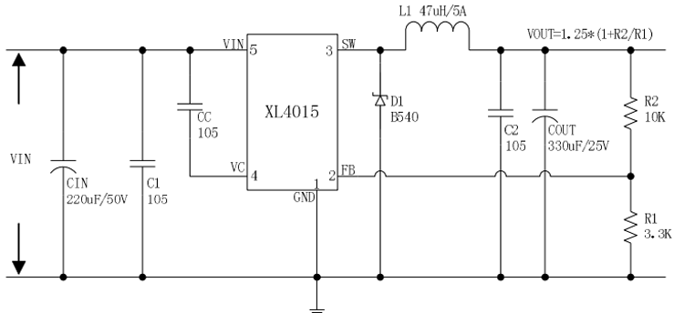
Now compare the above schematic to our schematic, you can see that it's very similar because the schematic for the buck regulator portion stays the same, the only additional difference is that it has additional current limiting functionality.
Current Limiting Circuit with TL431
Now, let's understand how the current limiting functionality works. In the schematic, you can see we have a 78L05 Voltage Regulator, which is an ultra-low-power regulator that is used to convert the input voltage to a constant 5V for the TL431 IC. The TL431 is a reference that is set to a constant current regulator mode with the help of a 71.5K resistor and a potentiometer. This reference is compared to the sense voltage from the output side of the resistor to limit the current. The circuit shown below is the TL431 circuit that is providing a constant current source to the op-amps.
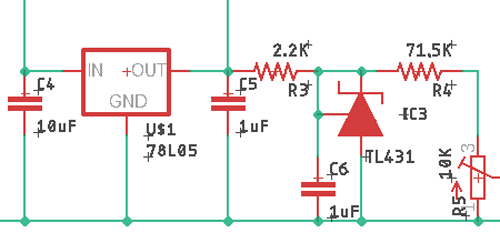
Next, we have the first op-amp portion; this portion of the circuit is actually used to limit the current. What happens in this portion is that the output sense voltage gets compared with the reference voltage from the TL431 IC. Next, what happens is that if the output sense voltage is greater than the reference voltage, the output of the op-amp turns high, and with the shutdown function of the circuit, the output of the IC turns off.
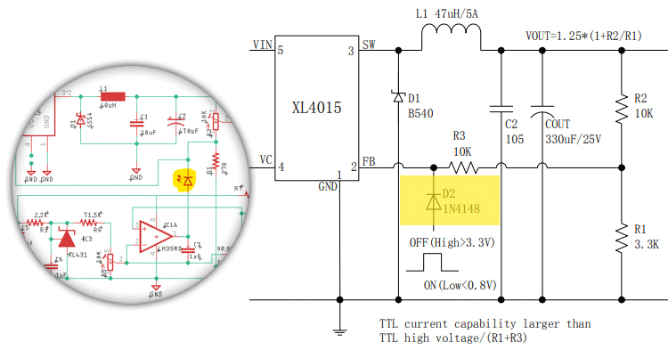
In the above image, I have shown you an application circuit from the datasheet with a practical circuit side by side. So in the practical circuit, the manufacturer uses an LED instead of a diode; this LED not only acts as a reverse current blocking but also lights up when the current limit function is active.
Battery Charging Indication System
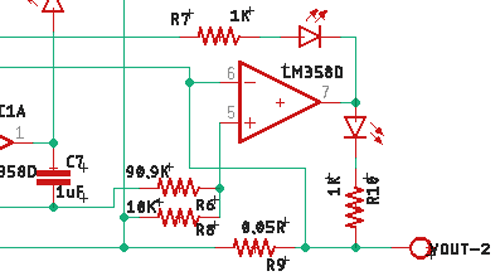
Next, we have the final portion of the circuit. This portion of the circuit is used to indicate the battery charging and fully charged condition. In this circuit, when the battery is fully charged, the output goes low, so the charging complete LED turns on. Now, if a battery is charging, the other LED turns on to indicate the battery is charging.
Recreating the PCB for XL4015 Buck Converter
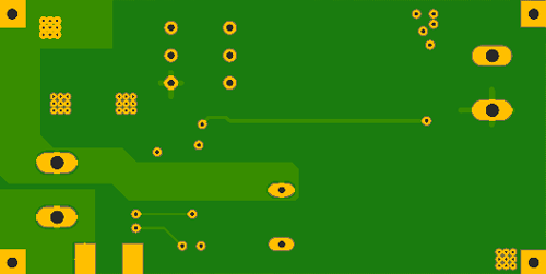
As we have already made the schematic, we thought to recreate the PCB for the buck converter modules, and we did just that. The dimension of the PCB is 25mm / 50mm. Proper PCB layout is crucial for optimal dc dc buck converter performance. You can see that from the image below.
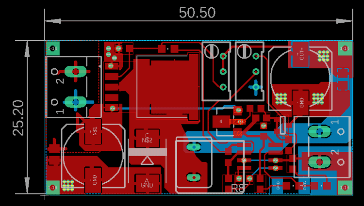
Next, we have used the Manufacturing functionality of Eagle to determine the top and bottom portions of the PCB, and it looks like something that is shown below.
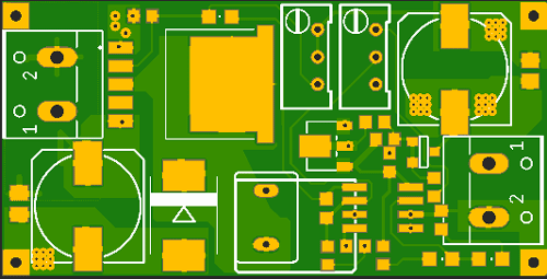
In the above image, the TOP side of the PCB is shown, and the bottom side of the PCB is shown below-
That's all for the PCB part, and you can download the Gerber file for the project by clicking the given download link.
Testing the XL4015 DC-DC Buck Converter Module
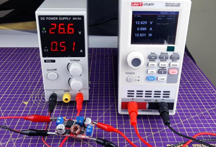
To start the test, we first connect the buck converter module to the power supply and connect the output to the DC load, and we have set a constant load of 1A to test the circuit. Comprehensive testing validates the XL4015 buck converter performance against datasheet specifications.
Now as that was working, we set the constant current to 5A as it was advertised in the datasheet.
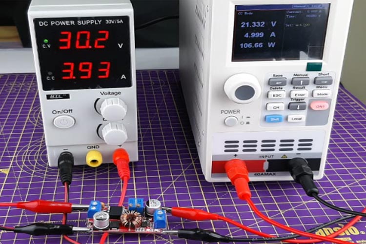
If you consider the size of the module, I was very impressed to see that it was able to deliver a constant current of 5A. I tested this circuit for 5 minutes, and it was working absolutely fine. During testing, several common issues were identified with simple solutions that improve the DC to DC buck converter circuit reliability.
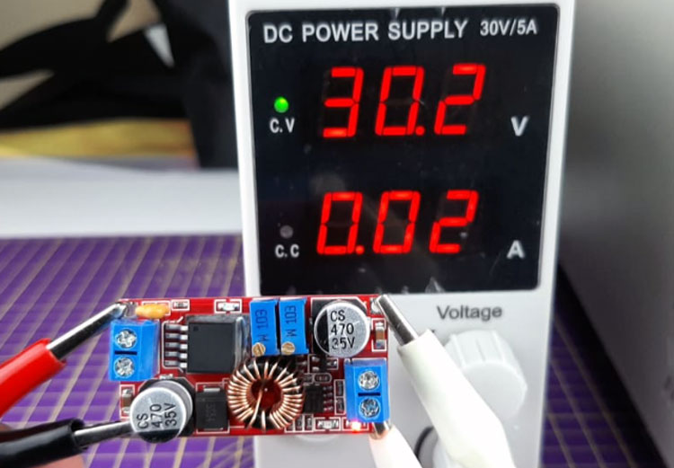
Next, we tested this circuit for short circuit conditions. As advertised on the datasheet, it has built-in short circuit protection, so we also tested that. And it worked absolutely fine.
Problems Encountered while Testing the Buck Converter Circuit
While testing the circuit, we encountered a major problem in some of these modules. At the time of writing the article, we had 10 modules in our lab, but some of those were working, and some of those were not. This made us very confused. The versatile dc to dc buck converter module serves multiple applications in power electronics, from simple voltage regulation to complex battery management systems
But the solution to this problem was very simple: we connected a 1uF capacitor to the PCB, and the module worked absolutely well without any issues. Other than that, we did not find any problems with the module board. The basic XL4015 buck converter circuit diagram can be enhanced with additional features for specific applications, including remote voltage sensing, synchronised switching, and enhanced protection.
Conclusion
The XL4015 demonstrates excellent performance as a versatile dc dc buck converter solution. I tested the module under various input/output voltages and load conditions and evaluated its efficiency, and all the tests went smoothly without any issues. So we can say that the XL4051 is a very cost-efficient and highly effective module for demo projects and battery charging.
Frequently Asked Questions on DC- DC Buck Converter
⇥ 1. What is the function of the XL4015 DC-DC buck converter?
The XL4015 operates using PWM switching to control a single internal MOSFET. The device energy is stored in the inductor during the on-time and then released when the internal switching diode during the off-time. The XL4015 allows a higher input voltage to be reduced in a regulated way to a lower output voltage.
⇥ 2. What input voltage range does the XL4015 buck converter work with?
The XL4015 buck module has input voltage specifications from 8V - 36V DC. These voltage specifications make it applicable to automotive, industrial, and battery-powered applications where input voltages may vary a lot.
⇥ 3. How can I program the constant current and voltage on the XL4015 module?
The XL4015 has two 10K multi-turn potentiometers, one for setting the constant voltage (CV) mode from 1.25V-32V and the other to set the constant current (CC) limit at 0.2A-5A. You will want to adjust the potentiometers while monitoring with suitable test equipment.
⇥ 4. How efficient is the XL4015 buck converter?
Typically, the XL4015 buck converter can get to 96% efficiency under optimal conditions, usually at a load of between 50-80%. The actual efficiency when booting up will always be based on the voltage difference from input to output, load current and component quality.
⇥ 5. Can I use XL4015 to charge lithium batteries?
Yes, the XL4015 has the CC/CV features required for lithium battery charging. Constant current for the bulk charging phase and constant voltage for the absorption phase, and even LED charge indicates!
⇥ 6. What protection features does the XL4015 buck converter have?
The XL4015 buck converter has a thermal shutdown feature, current limiting feature, short circuit protection and an undervoltage lockout feature. These features protect users against overcurrent, overtemperature and short circuit conditions that could potentially damage devices.
Hands-on Projects Related to DC-DC Conversion
The DC-DC Converter has been featured in many of our practical projects. We’ve utilised DC-DC Converters in several innovative projects, so you can explore them through the links below.

DC-DC Buck Converter Circuit - How to Step Down DC Voltage
In this project, we are going to make a Buck Converter Circuit using Arduino and an N-Channel MOSFET with a maximum current capacity of 6 amps. We are going to step down 12V DC to any value between 0 and 10V DC. We can control the output voltage value by rotating the potentiometer.
A Simple DC-DC Boost Converter using 555 Timer IC
In this project, we build a boost converter circuit using a 555 timer IC. A boost converter is a non-isolated type of switch-mode power supply that is used to step up the voltage. In other words, it gives a higher output voltage compared to the input voltage. The circuit is very similar to a buck converter we designed for controlling a motor and an LED strip, which is used to lower the incoming voltage.

Variable Output Voltage DC to DC Boost Converter using MC34063
In the previous tutorials, we demonstrated the detailed design of a 3.7V to 5V Boost Converter using MC34063 and a 12V to 5V Buck Converter using MC34063. Today, we will use the same MC34063 IC to build a DC to DC Boost Converter circuit, which can convert a small voltage, like 3V, to a higher voltage up to 40V. So here the MC34063 IC is used as an Adjustable DC-DC Converter.
Comments
EASYEDA PLEASE
Hi, I really Like your article it elucidates much of how the XL4015 buck converter circuit works. I was trying to understand your schematic for the board, but was a bit confused How the 7805 linear regulator and TL431 were connected to the lm358 op amp. Is there an EasyEDA file you can post that we could look at to understand the circuit better? Thanks
Hi, thank you for the post. It's very helpful. I have a small question: If my load consists of smart LEDs and I don't need to charge a battery, can I ignore the second part of the op-amp circuit entirely? I am still interested in using LM358 because of its availability and low cost.

Hey first of all very nice work i really like it. Can you files also i wanted to assemble this pcb via JLCPCB can i get some more files XD if guys don't mind.