
In this project we build a boost converter circuit using a 555 timer IC. Boost converter is a non-isolated type of switch mode power supply that is used to step-up the voltage. In other words, it gives a higher output voltage compared to the input voltage. The circuit is very similar to a buck converter we designed for controlling motor and LED strip which is used to lower the incoming voltage. Boost converters find usage in a lot of our daily equipment, these are very common power electronics circuits which are used extensively with the solar panels and other harvesting technology, and are one of the most important circuit in today’s time. In this article, we will learn about buck converters and design a very simple boost converter using 555 timer and IRFZ44N, N-channel MOSFET. You can check simple and interesting power electronics circuits here.
Working of a DC-DC Boost Converter
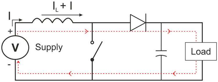
The boost converter is used to increase the output voltage by reducing the current, this is achieved by storing energy in an inductor and since the energy in an inductor cannot change instantly therefore, it starts storing the energy in its magnetic field. Current across the inductor is given by Iinductor = V/R and since the resistance and current is constant, the only value which can change is the voltage. As shown in the figure below, an inductor is connected in series with the voltage source to constantly turn on and off a circuit a switch is connected in parallel to the voltage source and inductor for achieving fast switching we utilize a MOSFET along with a MOSFET driver. The circuit is connected to a load and a capacitor in parallel to it. In order to stop the current flowing backwards from the capacitor, a diode is used between the capacitor and the MOSFET.
The inductor tries to resist change in the current to provide a constant input current and hence the Boost converter acts as a constant current input source, while the load acts as the constant voltage source, this circuit is very similar to the buck converter and is sometimes called backward buck converter. The N-channel MOSFET is controlled by a PWM signal, we have used IC 555 timer to provide the output to the MOSFET. The capacitor is used to store the charge and provide a constant output to the load. The circuit works in 2 stages, in the 1st stage, the switch is turned on and in the 2nd stage, the switch is in the off stage.
Stage 1: Switch is on: Charging mode
In this condition the MOSFET switch is turned on. The MOSFET we have used is a N-channel IRFZ44N MOSFET, with its gate pin connected to the pin 3 of the IC555 timer. When the switch is in ON state, it completes the circuit across the inductor and the voltage is applied across it which results in a magnetic field around it. Since it offers a very low resistance path, all the voltage flows through the switch and goes back to the supply as marked by the red line in the figure below.
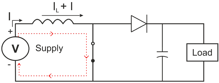
The capacitor which was previously charged during the last on stage tries to discharge itself from the MOSFET and to stop it, we use a diode in order to stop the charge from capacitor flowing in the reverse direction.
Stage 2: Switch is off: Discharging mode
When the switch is in the off state, the inductor’s charging path is not completed, hence the polarity of inductor is reversed and the magnetic field around it collapses as a result a voltage surge is generated which passes through the diode and charges the capacitor. The cumulative energy from inductor and source is used to charge the capacitor as well as runs across the load.
Duty Cycle:
The total time of a switching cycle is called time period (T), the on time and off time of the switch is given by Ton and Toff respectively. Therefore:
T = Ton + Toff
Frequency (f) is given by-
f = 1 / (Ton + Toff)
Duty cycle (D) is given by the total time for which the switch is on with respect to the total time period. Duty cycle is given by:
D = Ton / T
Using the Kirchoff’s Voltage Law, we can derive the steady state of a boost converter. Here, we will consider that the circuit is an ideal circuit and no power is lost during the whole process that is:
Vin = Vout
Theoretically, in one complete cycle, the net change of inductor current is zero and the ratio of input voltage Vin to the output voltage (Vout) is given by:
Vin / Vout = 1 / (1-D)
Theoretically, 0 < D <1 but if we assign 1 as duty cycle, then the ratio will become infinite which is impossible to achieve.
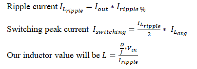
Calculating value of Inductor:
We know that average input current (Iavg) is equal to average inductor current (ILavg). Therefore, the average inductor current can be calculated by:
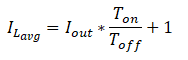
Inductor’s ripple current is typically 20-40% of the average output current.
Calculating Charging Capacitor:
Calculating charge time of capacitor Tc = R*C
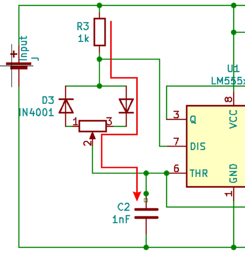
Here, the R is the resistance of the charging circuit, and C is the capacitance of the capacitor. In our circuit given below, the charging circuit follow the path marked in red, i.e. R3 > D2 > C2.
To calculate the values of input resistor and capacitor, you can also use this online calculator.
Calculating Output Capacitor:
Selection of Components
I designed the circuit on Eschema, KiCad and did calculation for the required components by using the above formulae. I then made the circuit on the bread board. The circuit diagram designed in KiCad is given below.

Components required:
- 1 x NE555
- 1 x IRFZ44N – N Channel MOSFET
- 1 x 100uH, Inductor
- 1 x 1K, Resistor
- 2 x IN4001 Diode
- 1 x IN5822 Diode
- 1 x 100nF, Capacitor
- 1 x 1nF Capacitor
- 1 x 50k potentiometer
- 2 x 2pin connector (for connecting input and output from the circuit)
Things to remember while selecting the component:
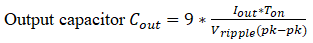
MOSFET: you need to select a MOSFET which will be able to withstand the maximum output voltage, therefore the breakdown voltage of it should be higher than the max output of the converter.
Diode: For low voltage operations, I have used the IN5822 because the slow speed of 1n4007 makes it unusable for our operations. We need to select a fast diode, I tried using a 1n4007 diode as the output diode but due to the performance issue, I changed to a faster IN5822.
Working of Boost Converter Circuit
The circuit uses the 555 IC in astable mode as the PWM generator and hence the whole circuit is based around the same. The connections of all the 8 pins are mentioned below:
- Pin 1 is connected to the ground rail.
- Pin 2 and pin 6, with the ground through a 1nF capacitor.
- Pin 3 is giving the output signal and thus it is connected to the gate of the IRFZ44N, N-Channel MOSFET. This pin is responsible for driving the pwm output to the gate of the MOSFET.
- Pin 4 need to be connected to the power supply
- Pin 5 is helping in stabilizing the output and thus it is connected to the ground through the 0.01 uF capacitor. It also helps in providing immunity against electrical noises.
- Pin 7 is connected to the inverted diode setup; the junction is connected to the positive rail through a 1K resistor.
- Pin 8 needs to be connected to the power supply.
The main component in any SMPS is the switch, here in this circuit we are using the N-channel MOSFET, IRFZ44N as a switch. It is driven by the faint signal from IC 555, therefore the gate of IRFZ44N is connected to the 555IC. Drain is providing the negative switching control to the circuit and the source is connected to the ground. It has the following specification
VDSS = 55V
RDS(on) = 17.5mΩ
ID = 49A
Testing 555 Timer based Dc Dc Boost Converter Circuit
I tested the circuit with a 3.7V Li-ion cell, the cell was charged to about 3.4V. I connected the cell to the boost converter and the voltage across it showed a reading of 7.5V. The image of output across the output of boost converter is shown below.
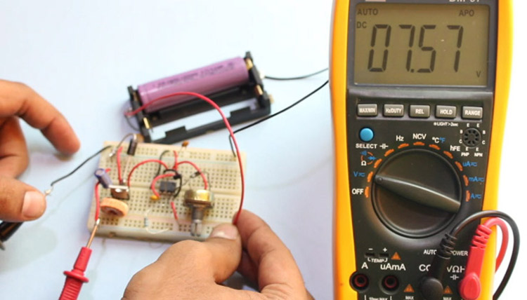
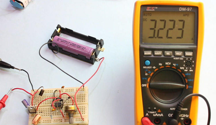
To test the current, I changed the lead of the multimeter to the current probe (do remember to select 10A or 20A setting on your multimeter to protect it from getting damaged.) the current was showing 3.2 Amps, thus this circuit is capable of producing around 30Watts. The circuit did work properly and was able to boost the voltage.
The lack of feedback causes the circuit to drop voltages when a load is connected across it. The feedback employed by boost converters make sure that the duty cycle remains stable even when the load is connected. We can easily provide feedback by using a microcontroller to measure change in output and then changing the input resistance, thus making this circuit more useful and practical for most of the operations.
This is a very simple yet effective circuit which can be used if you need a higher voltage then your voltage source can provide while reducing power wastage in your circuit. This circuit was able to give power over 30W. Although, it is advisable to use at least a perf board to create the circuit as regular bread boards are meant for low powered application. If you need a constant output, you should use fixed resistor in place of the pot to improve the overall design efficiency. The main drawback of this circuit is that due to the lack of feedback, the voltage drop is quite substantial when you connect the load. The final word is that it is a fun to build circuit which can be designed by simple components we all have lying at our work desk.
If you have any questions or doubt regarding this article, please feel free to use our Forum or you can leave your comments below.

Nice!! i will be testing that one for sure, thanks!! By the way, i just noticed that you're missing C3 in your parts list(100uf cap)!! :p