

In the world of flip-flops, the Clocked JK Flip Flop stands out with its outstanding features, such as all usable input states and the ability to be modified to imitate other flip-flops like SR, T, and D. This makes the JK Flip Flop a little better than the others. It's often called a universal flip-flop.
The JK flip-flop's main advantage is its ability to handle all possible input combinations without any issues. This includes a useful toggle operation that makes it essential for counter JK flip flop applications, frequency dividers, and memory circuits. You'll find JK flip-flops in many everyday electronics, from the timing circuits in microprocessors to LED flashers in gadgets. They're commonly used in digital counters, frequency synthesisers, and control systems for various applications.
This comprehensive guide covers everything about the JK flip flop circuit diagram, including detailed implementations using NAND and NOR gates, the complete clocked JK flip flop truth table, and practical applications in modern digital systems.
Table of Contents
Clocked JK FlipFlop
This Clocked JK Flip-Flop can be referred to by multiple names like JK Flip-Flop, Clocked JK Latch, or Clocked JK Flip-Flop. These variations mostly come from naming confusion. In general, a latch is a combinational circuit that requires no clock pulse, whereas a flip-flop, on the other hand, needs a clock to function. That’s why the term “Clocked” is often added, making it a Clocked JK Flip-Flop.
This Clocked JK Flip-Flop has two inputs, J and K, which function similarly to the Set and Reset inputs in an SR flip-flop, but with a smart upgrade. When both J and K are held HIGH, instead of entering an invalid or unstable state (as seen in the SR flip-flop), the JK flip-flop simply toggles its output with each edge-trigger pulse.
Key Features of JK Flip Flop
- No Invalid States: Unlike SR flip flops, all four input configurations (00, 01, 10, 11) will output valid, predefined states for outputs.
- Toggle: When both JK=1 and K=1, the output toggles on each clock transition, making it well-suited for counter JK flip flop applications.
- Universal Device: A JK flip flop can be configured to mimic the SR, D, and T flip flops with appropriate connections to the inputs.
- Edge-Triggered: It only responds to clock transitions (rising or falling edge), which avoids race conditions.
Clocked JK Flip Flop Truth Table and Working Principle
Understanding the clocked JK flip flop truth table is essential to explain the working of the JK flip flop. To fully explain the working of the JK flip flop, it's essential to understand both the internal logic operation and the external behaviour. For reference, you can see the basic symbol and the Clocked JK flip flop truth table below.
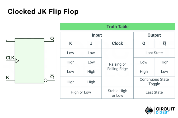
Here, you can easily understand the Clocked JK Flip Flop by observing the truth table. Below, you can see a brief explanation of the working of the Clocked JK Flip Flop.
Detailed Working Explanation of Each State
| J = 0, K = 0 ("00") |
|
| J = 0, K = 1 ("01") |
|
| J = 1, K = 0 ("10") |
|
| J = 1, K = 1 ("11") |
|
Clock is stable (no edge), J or K can be anything |
|
Now you should have some idea of how the JK Flip Flop works. Next, let’s look at the Clocked JK Flip Flop circuit diagram.
Advantages of Clocked JK Flip-Flops in Digital Design
The clocked JK flip flop offers several critical advantages that make it the preferred choice for many digital applications.
» No Invalid States: Unlike SR flip-flops, JK flip-flops eliminate forbidden input combinations.
» Toggle Functionality: Built-in toggle capability when both J and K inputs are high.
» Universal Flip-Flop: Can be configured to emulate SR, D, and T flip-flops.
» Edge-Triggered Operation: Synchronous operation with clock edges prevents timing race conditions.
» Memory Capability: Holds the previous state when both inputs are low effectively.
» Versatile Input Control: Four distinct input combinations provide complete output state control.
» Clock Synchronisation: All state changes occur synchronously with clock signal transitions.
Clocked JK Flip Flop Logic Diagram
The JK flip flop using NAND gate is the most common implementation in digital circuits. In real time, there are many simple ways to achieve the JK Flip Flop, such as a Clocked JK Flip-Flop using NAND gates, a Clocked JK Flip Flop using NOR gates, or a Clocked JK Flip-Flop using a dedicated Integrated Circuit chip like the 74LS76.
Let’s go through all three in simple terms.
1. Clocked JK Flip Flop Circuit Diagram Using NAND Gate
To create a JK Flip Flop using NAND gates, we need a total of six 2-input NAND gates. The JK Flip Flop circuit diagram looks like this:
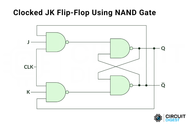
In some places, you might also see a simplified diagram that uses 3-input NAND gates. That works too, but based on my experience with simulation, the 2-input NAND configuration works better than the 3-input version. You can read more about these details in one of our articles, Flip-Flop in Digital Electronics: Types, Truth Table, Logic Circuit and Practical Demonstration, which explains all types of flip-flops. You can use clock buffers for driving multiple JK flip flop using NAND gate circuits.
Internal Operation of JK Flip Flop Logic Gates
The working is the same as a regular JK Flip-Flop.
- When J = 0 and K = 0, the flip-flop does nothing on a clock edge. It simply holds on to its previous state. This is called the memory or no-change condition.
- When J = 0 and K = 1, the flip-flop resets on the clock edge. The output Q becomes 0, and Q̅ becomes 1.
- When J = 1 and K = 0, the flip-flop sets on the clock edge. The output Q becomes 1, and Q̅ becomes 0.
- When J = 1 and K = 1, the flip-flop toggles its output every clock edge. If Q was 0, it becomes 1, and if Q was 1, it becomes 0. This toggle action is commonly used in JK Flip Flop counters.
- If the clock is stable (not changing), the outputs remain the same no matter what J and K are. A JK flip-flop only changes state when the clock edge occurs.
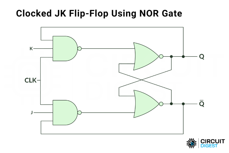
2. Clocked JK Flip Flop Using NOR Gate Configuration
When creating a JK Flip Flop using NOR gate, not all NAND gates are replaced with NOR gates. Instead, only the two NAND gates at the output (Q and Q̅) are replaced with NOR gates, while the input stage remains with NAND gates. However, the NAND gate versions are more commonly used and preferred.
NOR Gate vs NAND Gate Implementation
| Aspect | NAND Gate Implementation | NOR Gate Implementation |
| Popularity | Most widely used in industry | Less common, specialized applications |
| Gate Count | 6 NAND gates (2-input) | 4 NAND + 2 NOR gates |
| Power Consumption | Generally lower in CMOS | Slightly higher due to mixed gates |
| Signal Polarity | Active-low internal signals | Active-high output latch |
| PCB Layout | Simpler with single gate type | More complex routing |
The JK flip flop circuit diagram using NOR gates follows the same functional behaviour as the NAND implementation. Above, you can see the logic diagram of the Clocked JK Flip Flop using NOR gate. It follows the same logic as the general JK Flip-Flop, so I didn’t repeat the explanation here. You can refer to the above section for a better understanding. Understanding timing relationships is crucial to explain the working of JK flip flop.
3. Clocked JK Flip Flop IC Implementation: Integrated Circuit Solutions
These JK flip flop circuit ICs provide pre-tested, reliable functionality with built-in preset, clear, and timing features that simplify circuit design and reduce board space. While discrete JK flip flop using NAND gates and IC implementations remain common in education and simple circuits for modern digital design.
An example of such an integrated circuit (IC) is the 7476 IC. This chip contains two separate positive-edge-triggered JK flip-flops with individual J, K, clock, preset, and clear inputs. It’s a common choice for digital design projects where JK flip-flop behaviour is needed. When implementing a JK flip flop circuit diagram in your design, consider these important factors.
Popular JK Flip Flop ICs and Their Specifications:
| 7476 IC: | Contains two JK flip-flops in one package. Each flip-flop has its own J, K, clock, preset, and clear input, making it versatile for toggling, setting, resetting, and memory operations. |
| 74LS76: | Similar to the 7476 but from the low-power Schottky (LS) TTL family. Features dual JK flip-flops with set and clear functions, commonly used in TTL logic circuits. |
| CD4027: | CMOS implementation of two JK master-slave flip-flops. Each flip-flop operates synchronously, making it useful for counters and registers in low-power or mixed-signal designs. |
| 74LS112: | Another TTL-based chip with dual JK flip-flops, each featuring preset (set to 1) and clear (reset to 0) controls for more direct state management. |
How to Choose a JK Flip Flop IC
Key points to consider when making a JK flip flop circuit IC decision for your project:
- Power Supply Needs: CMOS (CD4027, 74HC73) for battery powered applications, TTL (7476, 74LS76) for circuits powered from a standard 5V power supply
- Speed Requirements: Schottky TTL if a frequency over 10MHz is desired
- Trigger Type: Depending on your system's timing, positive-edge (7476) or negative-edge triggered (74LS112)
- Style: DIP for a prototyping/breadboarding circuit, SOIC/TSSOP for standard production PCBs.
Practical Applications of Clocked JK Flip-Flops
The clocked JK flip flop finds widespread use across numerous digital applications due to its versatility and robust operation. All these ICs provide reliable JK flip-flop logic, making them useful for applications like:
1. Digital Counters: Binary counting circuits using toggle mode for sequential operations. The counter JK flip flop configuration represents one of the most common applications.
2. Frequency Division Circuits: Clock signal frequency division by factors of two repeatedly.
3. Shift Registers: Serial and parallel data shifting for communication and storage. JK flip flop logic gates form the core of shift registers used for:
4. Memory Storage Systems: Static RAM cells and buffer registers for data retention. The memory capability of the clocked JK flip flop truth table hold state makes it ideal.
Troubleshooting JK Flip Flop Circuits
| Symptom | Possible Cause | Solution |
| Output doesn't change | No clock signal or J=K=0 | Verify clock signal with oscilloscope; check input connections |
| Erratic output behavior | Clock noise or poor signal integrity | Add decoupling capacitors; improve clock signal quality |
| Outputs stuck HIGH or LOW | Power supply issue or damaged IC | Check power supply voltage; replace IC if necessary |
| Toggle mode not working | Incorrect feedback connections | Verify JK flip flop circuit diagram wiring; check output feedback paths |
Conclusion: Mastering the Clocked JK Flip Flop
The clocked JK flip flop is still one of the most fundamental building blocks in digital electronics since its flip flop capabilities are universal and have unmatched versatility. It has applications from a simple counter JK flip flop to complex state machines. Getting the circuit diagram of the JK flip flop, the truth table of the clocked JK flip flop, and implementations via NAND or NOR gates will provide an important education for any digital designer.
For educational purposes, implementing a JK flip flop using NAND gate, or selecting the proper IC for a production design, the principles presented in this document will provide access to implementing JK flip-flops in your designs.
Key Takeaways
- The JK flip flop is clocked to produce valid output states and allows for toggling functionality
- The clocked JK flip flop truth table must be understood to implement the circuit
- When using a JK flip flop with NAND gates, six 2-input gates are needed
- Edge-triggered produces a synchronous/certain change of state
- Various applications can be made from counters, frequency dividers, memory and control
- Consider timing parameters to prevent unwanted state changes of metastability and ensure reliability.
This tutorial was created by the Circuit Digest engineering team. Our experts focus on creating practical, hands-on tutorials that help makers and engineers master Raspberry Pi projects, Arduino projects, Electronic circuits and IoT development projects.
I hope you liked this article and learned something new from it. If you have any doubts, you can ask in the comments below or use our forum for a detailed discussion.
Frequently Asked Questions About Clocked JK Flip Flops
⇥ 1. What happens when both the J and K inputs are high in a clocked JK flip-flop?
When both J=1 and K=1, a clocked JK flip-flop is in toggle mode. The output changes state on every opponent time to a positive or falling clock edge: Q changes to Q̅ and vice versa. The toggle capability is standard practice in counter physically, and clocked JK flip-flops are used as frequency dividers.
⇥ 2. How many NAND gates would be needed to implement a JK flip-flop?
A typical JK flip-flop can utilise six NAND gates: four for the input conditioning stage of the flip-flop and two for the cross-coupled outputs for the capacitance latch. Some designs use 3-input NAND gates, where only four are needed when two are used for cross-coupling, but the speed of the 2-input NANDs makes them preferable.
⇥ 3. What function does the clock input have in a clocked JK flip-flop?
The clock inputs times the state changes to specific time intervals, allowing a clocked JK flip-flop to change outputs only on clock edge transition (positive or negative). The edge-triggered operation avoids timing hazards with sequential logic, preventing race conditions, and allows for synchronous operation in larger digital systems.
⇥ 4. Can a JK flip-flop function as a frequency divider?
Yes! The JK flip-flop counter arrangement will divide frequencies by 2 when J=1 and K=1. The output will change state with every clock pulse, resulting in the output frequency being half the frequency of the input clock. By cascading together multiple stages, larger division ratios can be achieved (÷4, ÷8, ÷16, ...).
⇥ 5. What is the difference between master-slave & edge-triggered JK flip-flops?
The circuit diagram configurations for master/slave JK flip-flops think in terms of two stages (master/slave) and will update in sequence for times of clock HIGH and LOW, whereas edge-triggered JK flip-flops will respond to the clock only at the moment of transition. Edge-triggered devices (7476 is an example) are faster, and also more widely used for synchronous designs that are in favor today.
⇥ 6. How do you convert/from JK flip-flops to some of the other types of flip-flops?
To get D flip-flops, tie the disadvantaged K input to the inverted J (K=J̅) and supply the data to J. To create T flip-flops, connect both J and K to HIGH, or toggle input. To get vanilla SR flip-flop action, utilise J as Set and K as Reset, and supply the inputs appropriately.
⇥ 7. What are the timing parameters associated with the operation of the JK flip-flop?
The critical timing specifications to be aware of are setup time (amount of stability of the inputs before the clock edge, usually 20 to 50ns), hold time (amount of stability of the inputs after the clock edge, usually 5 to 20ns), propagation delay (how long it takes to get input to output, from the clock to output, usually 10 to 25ns) and the minimum clock pulse width. If these specifications are violated, unreliable operation or metastability may occur.
Common Types of flip-flops
There are several types of flip-flops in digital electronics, each designed to perform specific functions in storing and controlling data. While they all operate on the basic principle of bistable states, their input configurations and applications vary. The most common types are:

SR Flip-Flop with NAND Gates: Circuit, Truth Table and Working
Understand the SR flip-flop built with NAND gates, including its logic circuit, truth table, and working using IC SN74HC00N.

JK Flip-Flop: Circuit, Truth Table and Working
Explore the JK flip-flop, its truth table, circuit logic using NAND gates, and practical implementation with the MC74HC73A dual flip-flop IC.

D Type Flip-Flop: Circuit, Truth Table and Working
Learn how a D-type flip-flop works, including its clock-dependent behaviour, truth table, and logic implementation with NAND gates or the HEF4013BP dual flip-flop IC.

T Flip-Flop: Circuit, Truth Table and Working
Explore the T (Toggle) flip-flop, its logic circuit using NAND gates, truth table, and its behaviour when paired with the MC74HC73A dual JK flip-flop IC.
