

Power Supply Unit (PSU) is a vital part in any electronic product design. Most household electronic products like Mobile Chargers, Bluetooth Speakers, Power Banks, Smart Watches etc requires a Power Supply circuit that could convert the AC mains supply to 5V DC to operate them. In this project we will build a similar AC to DC power supply circuit with 10W power rating. That is our circuit will convert the 220V AC mains to 5V and provide a maximum output current upto 2A. This power rating should be enough to power most electronic products running on 5V. Also 5V 2A SMPS circuit is quite popular in electronics since there are lots of microcontrollers which operates on 5V.
The idea of the project is to keep the build as simple as possible, hence we will design the complete circuit over a dotted board (perf board) and will also build our own transformer so that anyone could replicate this design or build similar ones. Excited Right! So lets get started. Previously we have also built a 12V 15W SMPS circuit using a PCB, so people who are interested in how to design a PCB for a PSU project (power supply unit) can check that as well.
5V 2A SMPS Circuit – Design Specifications
Different varieties of power supply behave differently in different environments. Also, SMPS works in specific input-output boundaries. Proper specification analysis needs to be performed before going forward with the actual design.
Input specification:
This will be an SMPS in AC to DC conversion domain. Therefore, the input will be AC. For the input voltage value, it is good to use a universal input rating for the SMPS. Thus, the AC voltage will be 85-265VAC with 50Hz rating. This way the SMPS can be used in any country irrespective of their AC mains voltage value.
Output specification:
The output voltage is selected as 5V with 2A of the current rating. Thus, it will be 10W output. Since this SMPS will provide constant voltage irrespective of the load current, it will work on the CV (Constant Voltage) mode. This output voltage of 5V should be constant and steady even at the lowest input voltage during a maximum load (2A) across the output.
It is highly desired that a good power supply unit has a ripple voltage of less than 30mV pk-pk. The targeted ripple voltage for this SMPS is less than 30mV peak-peak ripple. Since this SMPS will be built in veroboard using a handmade switching transformer we can expect a slightly higher values of ripple. This problem can be avoided by using a PCB.
Protection features:
There are various protection circuits that can be employed in a SMPS for a safe and reliable operation. The protection circuit protects the SMPS as well as the associated load. Depending on the type, protection circuit can be connected across input or across the output.
For this SMPS, input surge protection will be used with a maximum operating input Voltage of 275VAC. Also, to deal with EMI issues, a common mode filter will be used for blanking out the generated EMI. On the Output side we will include short circuit protection, over-voltage protection, and over-current protection.
Selection of the Power Management IC
Every SMPS circuit requires a Power Management IC also known as switching IC or SMPS IC or Drier IC. Let’s sum up the design considerations to select the ideal Power Management IC that will be suitable for our design. Our Design requirements are
- 10W output. 5V 2A at full load.
- Universal input rating. 85-265VAC at 50Hz
- Input surge protection. Maximum input voltage 275VAC.
- Output short circuit, over-voltage and over-current protection.
- Constant voltage operations.
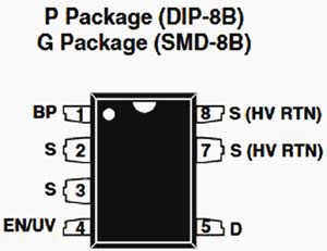
From the above requirements there is wide range of ICs to select from, but for this project we have selected Power integration. Power integration is a semi-conductor company that has a wide range of power driver ICs in various power output ranges. Based on the requirements and availability we have decided to use the TNY268PN from tiny switch II families. We have previously used this IC to build a 12V SMPS circuit on a PCB.

In the above image, the maximum power 15W is shown. However, we will make the SMPS in the open frame and for the universal input rating. In such a segment, TNY268PN could provide 15W output. Let’s see the pin diagram.
Designing the 5v 2Amp SMPS Circuit
The best way to build the 5V 2A SMPS Schematic is to use Power integration’s PI expert software. Download the PI expert software and use the version 8.6. It is excellent power supply design software. The Circuit shown below is constructed using Power Integration’s PI expert software. If you are new to this software you can refer to the design section of this 12V SMPS circuit to understand how to use the software.

Before going straight into building the prototype part, let’s explore the 5v 2A SMPS circuit diagram and its operation.
The circuit has the following sections-
- Input surge and SMPS fault protection
- AC-DC conversion
- PI filter
- Driver circuitry or Switching circuit
- Under-voltage lockout protection.
- Clamp circuit.
- Magnetics and galvanic isolation.
- EMI filter
- Secondary Rectifier and snubber circuit
- Filter Section
- Feedback section.
Input surge and SMPS fault protection:
This section consists of two components, F1 and RV1. F1 is a 1A 250VAC slow blow fuse and RV1 is a 7mm 275V MOV (Metal Oxide Varistor). During a high voltage surge (more than 275VAC), the MOV became dead short and blows the input Fuse. However, due to the slow blow feature, the fuse withstands inrush current through the SMPS.
AC-DC conversion:
This section is governed by the diode bridge. These four diodes (inside DB107) make a full bridge rectifier. The diodes are 1N4006, but standard 1N4007 can do the job perfectly. In this project, these four diodes are replaced with a full bridge rectifier DB107.
PI filter:
Different states have different EMI rejection standard. This design confirms EN61000-Class 3 standard and the PI filter is designed in such a way to reduce the common-mode EMI rejection. This section is created using C1, C2, and L1. C1 and C2 are 400V 18uF capacitors. It is an odd value so 22uF 400V is selected for this application. The L1 is a common mode choke that takes differential EMI signal to cancel both.
Driver circuitry or switching circuit:
It is the heart of an SMPS. The transformer's primary side is controlled by the switching circuit TNY268PN. The switching frequency is 120-132khz. Due to this high switching frequency, smaller transformers can be used. The switching circuit has two components, U1, and the C3. U1 is the main driver IC TNY268PN. The C3 is the bypass capacitor which is needed for the working of our driver IC.
Under-voltage lockout protection:
Under-voltage lockout protection is done by the sense resistor R1 and R2. It is used when the SMPS goes into the auto-restart mode and sense the line voltage. The value of R1 and R2 is generated via the PI Expert tool. Two resistors in series is a safety measure and a good practice to avoid resistor failure issues. Thus, instead of 2M, two 1M resistors are used in the series.
Clamp circuit:
D1 and D2 are the clamp circuit. D1 is the TVS diode and D2 is an ultra-fast recovery diode. The transformer acts a huge inductor across the power driver IC TNY268PN. Therefore during the switching off-cycle, the transformer creates high voltage spikes due to the leakage inductance of the transformer. These high-frequency voltage spikes are suppressed by the diode clamp across the transformer. UF4007 is selected due to the ultra-fast recovery and P6KE200A is selected for the TVS operation.As per the design, the targeted clamping voltage (VCLAMP) is 200V. Therefore, P6KE200A is selected and for ultra-fast blocking related issues, UF4007 is selected as D2.
Magnetics and galvanic isolation:
The transformer is a ferromagnetic transformer and it not only converts the high voltage AC to a low voltage AC but also provide galvanic isolation.
EMI filter:
EMI filtering is done by the C4 capacitor. It increases the immunity of the circuit to reduce the high EMI interference. It is a Y-Class capacitor with a voltage rating of 2kV.
Secondary Rectifier and Snubber Circuit:
The output from the transformer is rectified and converted to DC using D6, a Schottky rectifier diode. The snubber circuit across the D6 provides suppression of the voltage transient during switching operations. The snubber circuit consist one resistor and one capacitor, R3, and C5.
Filter Section:
The filter section consists of a filter capacitor C6. It is a Low ESR capacitor for better ripple rejection. Also, an LC filter using L2 and C7 provide better ripple rejection across the output.
Feedback section:
The output voltage is sensed by the U3 TL431 and R6 and R7. After sensing the line, U2, the optocoupler is controlled and galvanically isolating the secondary feedback sensing portion with the primary side controller. The Optocoupler has a transistor and a LED inside of it. By controlling the LED, the transistor is controlled. Since the communication is done by optically, it has no direct electrical connection, therefore satisfying the galvanic isolation on the feedback circuit too.
Now, as the LED directly controls the transistor, by providing sufficient bias across the Optocoupler LED, one can control the Optocoupler transistor, more specifically driver circuit. This control system is employed by the TL431. A shunt regulator. As the shunt regulator has a resistor divider across it reference pin, it can control the Optocoupler led which is connected across it. The feedback pin has a reference voltage of 2.5V. Therefore, the TL431 can be active only if the voltage across the divider is sufficient. In our case, the voltage divider is set to a value of 5V. Therefore, when the output reaches 5V the TL431 gets 2.5V across the reference pin and thus activate the Optocoupler's LED which controls the transistor of the Optocoupler and indirectly controls the TNY268PN. If the voltage is not sufficient across the output the switching cycle is immediately suspended.
First, the TNY268PN activates the first cycle of switching and then sense its EN pin. If everything is alright, it will continue the switching, if not, it will try once again after sometime. This loop gets continued until everything gets normal, thus preventing short circuit or overvoltage issues. This is why it is called flyback topology, as the output voltage is flown back to the driver for sensing related operations. Also, the trying loop is called a hiccup mode of operation on the failure condition.
The D3 is a Schottky barrier diode. This diode converts the high frequency AC output to a DC. 3A 60V Schottky Diode is selected for reliable operation. R4 and R5 is selected and calculated by the PI Expert. It creates a voltage divider and passes the current to the Optocoupler LED from the TL431.
R6 and R7 is a simple voltage divider calculated by the formula TL431 REF voltage = (Vout x R7) / R6 + R7. The reference voltage is 2.5V and the Vout is 12V. By selecting the value of R6 23.7k, the R7 became 9.09k approximately.
Building a Switching Transformer for our SMPS Circuit
Normally for an SMPS circuit a switching transformer will be required, these transformers can procured from transformer manufacturers based on your design requirements. But the problem here is if you learning stuff of building a prototype you cannot find the exact transformer off the shelves for your design. So we will learn how to build a switching transformer based on the design requirements given by our PI expert software.
Let's see the generated transformer construction diagram.
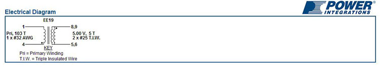
As the above image states we need to perform 103 Turns of single 32 AWG wire on the primary side and 5 turns of two 25 AWG wire on the secondary side.
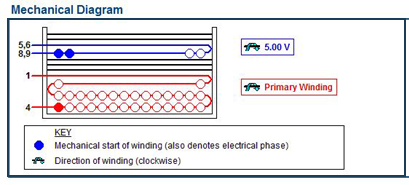
In the above image, starting point of the windings and the direction of the winding is described as a mechanical diagram. To make this transformer, the following things are needed-
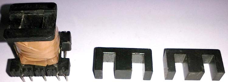
- EE19 core, NC-2H or equivalent specification and gapped for ALG 79 nH/T2
- Bobbin with 5 pins in the primary and secondary side.
- Barrier Tape with 1 mil thickness. 9mm wide tape is required.
- 32 AWG solderable coated enameled copper wire.
- 25AWG solderable coated enameled copper wire.
- LCR meter.
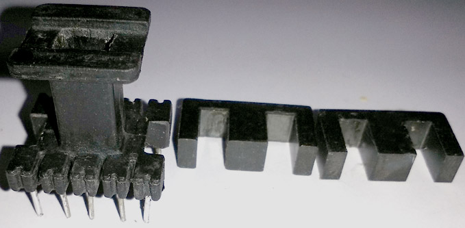
EE19 core with NC-2H with a gapped core of 79nH/T2 is required; generally, it is available in pairs. The bobbin is a generic one with 4 primary and 5 secondary pins. However, here bobbin with 5 pins on both sides is used.
For the Barrier tape, standard duct tape is used which has a base thickness of more than 1 mil (Typically 2 mil). During the tapping related activities, scissor is used to cut the tape for perfect widths. Copper wires are procured from old transformers and it can be purchased from local shops as well. The core and bobbin that I am using is shown below
Step 1: Add solder in the 1st and 5th pin on the primary side. Solder the 32 AWG wire at pin 5 and the winding direction is clockwise. Continue till the 103 turns as shown below
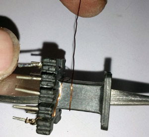
This forms the primary side of our transformer, once the 103 turns of winding are completed my transformer looked like this below.
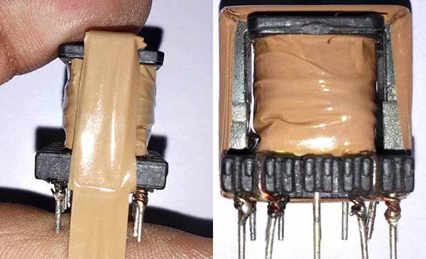
Step 2: Apply duct tape for insulation purposes, 3 turns of duct tape are needed. It also helps in keeping the coil in position.
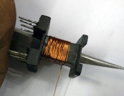
Step 3: Start the secondary winding from pin 9 and 10. The secondary side is made using two strands of 25AWG enameled copper wires. Solder one copper wire to the pin 9 and another one in pin 10. The winding direction is again clockwise. Continue till 5 turns and solder the endings on pin 5 and 6. Add insulating tape by applying duct tape same as before.
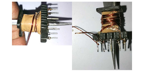
Once both primary and secondary windings are done and the duct tape was used, my transformer looked like as shown below
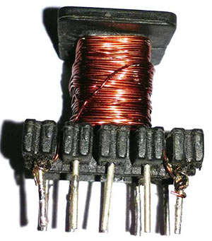
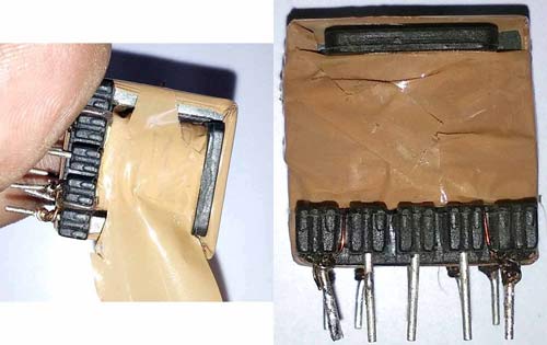
Step 4: Now we can secure the two cores tightly using duct tape.Once done the completed transformer should look like this below.
Step 5: Also make sure to wrap the duct tape side by side. This will reduce the vibration during high-density flux transfer.
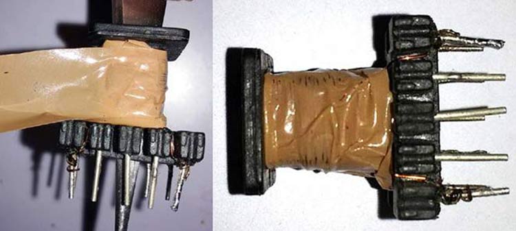
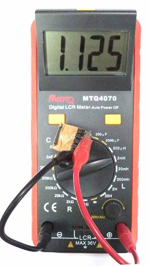
After the above steps are made and the transformer is tested using an LCR meter as shown below. The meter is showing 1.125 mH or 1125 uh inductances.

Building the SMPS Circuit:
Once the transformer is ready we can proceed with assembling the other components on the dotted board. The part detials required for the circuit can be found in th Bill of material list below
Once the components are soldered my board looks something like this.
Testing the 5V 2A SMPS Circuit
To test the circuit I connected the input side to the mains power supply through a VARIAC to control the input AC mains voltage. The output voltage at 85VAC and 230VAC is shown in the below-
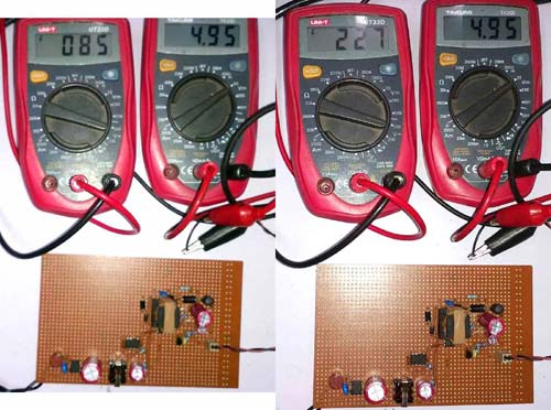
As you can see in both instances, the output voltage is maintained at 5V. But then I connected the output to my scope and check for ripples. The ripple measurement is shown below
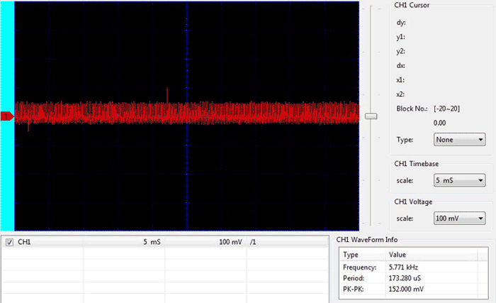
The output ripple is quite high, it shows 150mV pk-pk ripple output. This is totally not good for a power supply circuit. Based on the analysis the high ripple is due to the factors below-
- Improper PCB Designing.
- Ground bouncing issue.
- The PCB heat sink is improper.
- No cut-out on noisy supply lines.
- Increased tolerances on transformer due to hand winding. Transformer manufacturers apply dip varnish during the machine windings for better stability of the transformers.
If the circuit is converted to a proper PCB we can expect the ripple output of the power supply within 50mV pk-pk even with a hand-winding transformer. Yet, as veroboard is not a safe option for making switch mode power supply in AC to DC domain, it is constantly suggested that proper PCB must be established before applying high voltage circuits in practical scenarios. You can check the video at the end of this page to check how the circuit performs under load conditions.
Hope you understood the tutorial and learnt how to build your own SMPS circuits with a handmade transformer. If you have any questions leave them in the comment section below or use our forums for more questions.
Comments
Hi,
TNY268PN are not recommended new design.
I've found an SMPS IC for 5V / 500mA. The part is THX208 and its very suitable for IoT Applications low power solutions.
Is there any application examples for this IC or any recommended solutions for IoT applications.
There is some ready to use SMPS solutions but not reliable for final product.
"The D3 is a Schottky barrier diode. This diode converts the high frequency AC output to a DC. 3A 60V Schottky Diode is selected for reliable operation. R4 and R5 is selected and calculated by the PI Expert. It creates a voltage divider and passes the current to the Optocoupler LED from the TL431."
In this part, you have written that D3 diode is a Schottky barrier diode, can you please explain where we have to connect that D3 diode in the circuit because in the given circuit I didn't find it. please help!!!!!
Hello sir pls make a article or a video to explain how to choose component value in each section like pie filter, and other section .
Pls give me some advices and suggestions.
Please reply...

hi could anyone tell me alternative or availability of these components.i am trying to fix my power supply, transistors- h945 p 8b3
STTH1002CT GKDSNVU HIGH EFFICIENCY ULTRAFAST DIODE
STPS2045CT 75ACDVW SCOTTY - 2 of them.
thanks