

Most engineers who work with microcontrollers eventually run into the same challenge. A project needs to respond faster than firmware can, or it requires several digital signals to be combined in hardware. While these tasks can often be handled with interrupt service routines or external logic ICs, the solution quickly becomes complex as the design grows. This is where FPGAs excel, offering highly flexible hardware that can process multiple signals in parallel. However, for many beginners, the steep learning curve and relatively expensive development boards make getting started with FPGAs intimidating. The Microchip veryVerilog Kit offers a different approach. Instead of using a dedicated FPGA, it is built around the PIC16F13145, an 8-bit PIC microcontroller that includes a powerful peripheral called the Configurable Logic Block (CLB). While it isn't a replacement for a full FPGA, the veryVerilog Kit makes it much easier to start with FPGAs and Verilog programming.
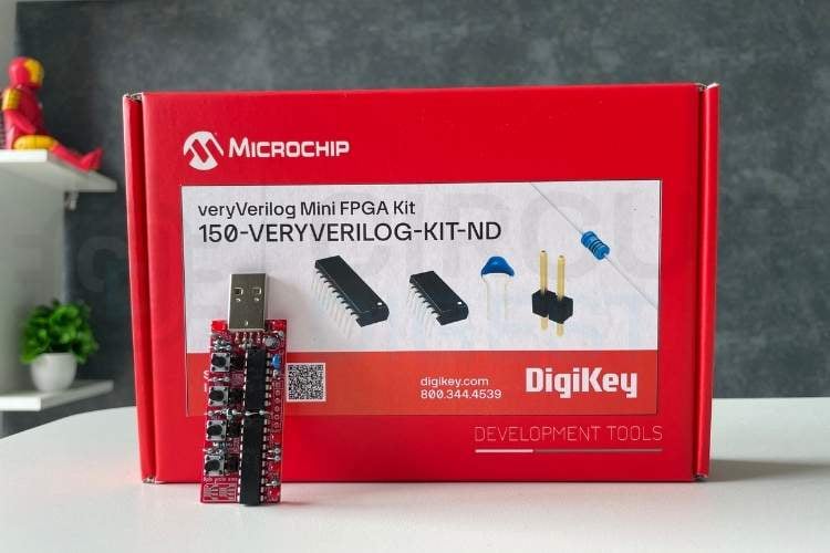
Developed in collaboration with DigiKey's Academic Program, the veryVerilog Kit is designed as an accessible introduction to digital hardware design. The board is supplied as a solder-it-yourself kit, making it an excellent learning platform from assembly through to programming. Once assembled, the onboard programmer allows the microcontroller to be programmed directly from a web browser, eliminating the need for an external programmer or complex software setup. In this article, we'll explore the fundamentals of FPGAs using the veryVerilog Kit. You'll learn what a Configurable Logic Block is, how it differs from a traditional FPGA, how the PIC16F13145 implements programmable hardware, and how to create basic digital circuits using the CLB. Starting with simple logic gates such as AND, OR, and NOT, we'll gradually combine them to build more complex digital logic while introducing key FPGA concepts including LUTs, flip-flops, routing, synthesis, and hardware configuration.
What is an FPGA?
Before diving into the veryVerilog Kit, it's helpful to understand the technology behind it. At the heart of the kit is a Configurable Logic Block (CLB), a peripheral designed to bring some of the flexibility of an FPGA into a microcontroller. To appreciate what makes the CLB special, let's first look at what an FPGA is and how it works.
FPGA stands for Field-Programmable Gate Array. Unlike a microcontroller, which executes instructions stored in memory one after another, an FPGA allows you to build custom digital hardware by configuring its internal logic resources. Instead of writing software that tells a processor what to do, you define the hardware itself, creating digital circuits that operate in parallel. A traditional microcontroller follows a familiar cycle: it reads an instruction, executes it, then moves on to the next one. Even with interrupts and multiple peripherals, there is still a central CPU making decisions. An FPGA works differently. Once configured, the hardware itself performs the required operations continuously, without relying on a processor to execute instructions.
For example, imagine you need an output to turn ON only when two input signals are HIGH. On a microcontroller, you would periodically read both input pins, compare their states in software, and update the output accordingly. On an FPGA, you simply create an AND gate in hardware. Whenever the inputs change, the output updates almost instantly, without any software involvement. This ability to execute multiple hardware functions simultaneously is what makes FPGAs well suited for high-speed digital signal processing, video interfaces, communication protocols, motor control, and other timing-critical applications. Although an FPGA may appear as a single chip from the outside, it is actually made up of thousands or even millions of tiny configurable logic resources connected through a programmable routing network. These resources can be combined in almost any way to create custom digital circuits.
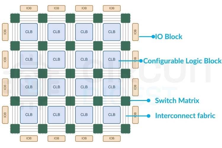
To understand how an FPGA works, it helps to become familiar with a few basic building blocks.
Basic Logic Elements (BLEs)
A Basic Logic Element (BLE) is the smallest programmable building block inside an FPGA. It typically consists of a Lookup Table (LUT) for implementing combinational logic and a Flip-Flop (FF) for storing the output of that logic when sequential operation is required. The LUT can be programmed to perform a wide range of logic functions, while the flip-flop allows the circuit to retain state and synchronize its operation with a clock signal. Depending on the application, the LUT output can either be used directly or passed through the flip-flop before being routed to other parts of the FPGA.
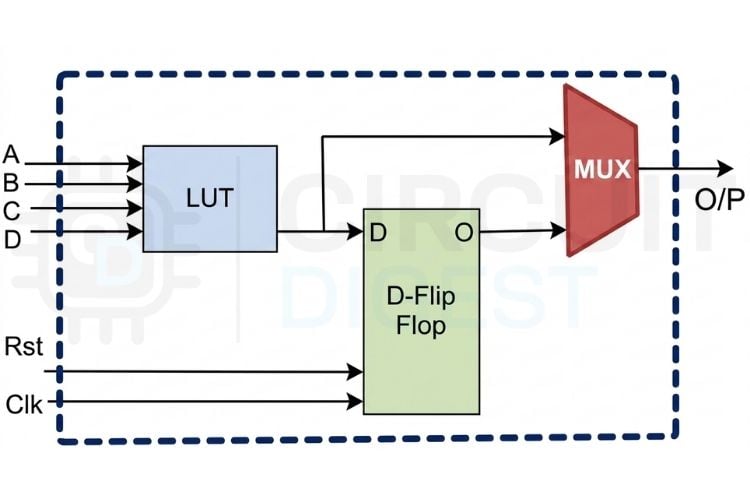
Individually, a BLE can only implement a relatively small piece of logic. However, by connecting many BLEs through the FPGA's programmable routing network, much larger and more sophisticated digital circuits can be created. In most FPGA architectures, multiple BLEs are grouped to form a Configurable Logic Block (CLB). The CLB provides additional local routing and shared resources, allowing the BLEs within it to work together efficiently. An FPGA is then built by arranging hundreds or even thousands of these CLBs in a programmable array, enabling designers to implement everything from simple logic gates to complex processors and communication interfaces.
Lookup Tables (LUTs)
A Lookup Table, or LUT, is the fundamental logic element inside most FPGAs. Rather than being a fixed logic gate, a LUT can be programmed to implement almost any Boolean function. For example, the same LUT can behave as an AND gate, an OR gate, an XOR gate, a NAND gate, or even more complex combinational logic involving multiple inputs. This flexibility is one of the reasons FPGAs are so versatile.
Routing Fabric or Interconnect Fabric
Logic elements alone aren't enough-they also need to be connected. Inside an FPGA, a programmable routing fabric acts like a network of tiny wires and switches that connect LUTs, flip-flops, memory blocks, and I/O pins. During synthesis, the FPGA development tools determine how these resources should be interconnected to implement your design. You can think of the routing fabric as the wiring between thousands of digital building blocks.
Configuration Bitstream
Unlike fixed-function ICs, an FPGA doesn't permanently contain your design. Instead, it is configured using a bitstream, a binary configuration file that tells the FPGA how every LUT, flip-flop, and routing switch should be programmed. Each time the FPGA powers up, this configuration is loaded into the device, transforming it into the custom hardware circuit you designed.
What is a Configurable Logic Block (CLB)?
A Configurable Logic Block (CLB) is a programmable hardware peripheral that is made up of multiple BLEs. Instead of executing software like the CPU, the CLB implements digital logic directly in hardware, allowing it to respond to events with deterministic timing and without consuming processor cycles. Although much smaller than a dedicated FPGA, the CLB follows the same principles. It contains programmable logic resources that can be configured to implement custom digital circuits such as logic gates, combinational logic, counters, state machines, pulse generators, signal conditioners, and timing circuits.
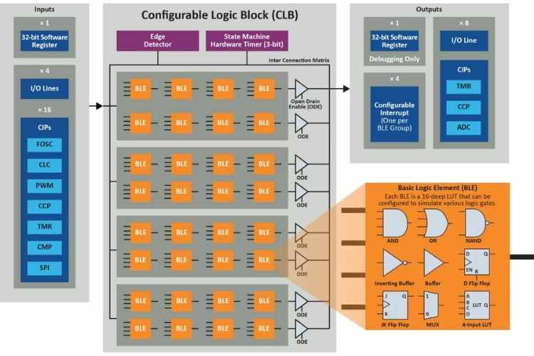
The CLB operates independently of the CPU. Once configured, it continuously processes its input signals and updates its outputs in hardware. This means the CPU is free to handle other tasks while the CLB performs repetitive or timing-critical operations in parallel. On the PIC16F13145, the CLB can interact with GPIO pins as well as several internal peripherals, allowing it to become part of the overall hardware architecture rather than just another software-controlled peripheral.
Why Put a CLB Inside a Microcontroller?
At first glance, adding programmable hardware to a microcontroller might seem unnecessary. After all, a CPU can already read inputs, process data, and control outputs through software. However, software isn't always the most efficient solution. Consider a simple example where an LED should turn ON only when two switches are pressed simultaneously. A microcontroller can certainly perform this task by repeatedly reading the input pins and updating the output. However, every input change requires CPU attention, even though the underlying logic is nothing more than an AND gate.
With a CLB, the same function is implemented directly in hardware. The two inputs are connected to an AND gate inside the CLB, and the output drives the LED. Whenever either switch changes state, the hardware responds immediately, without interrupting the CPU or executing a single line of firmware. As the logic becomes more complex, the advantages become even more apparent. Tasks such as signal debouncing, pulse generation, frequency division, protocol decoding, quadrature decoding, PWM shaping, or implementing small state machines can all be offloaded to the CLB. This reduces CPU workload, improves timing accuracy, and often simplifies the application software. The result is a system where software and hardware work together. The microcontroller handles high-level application logic and communication, while the CLB takes care of repetitive, deterministic digital operations.
Microchip veryVerilog Kit
Now that we've covered the basics of FPGA architecture and Configurable Logic Blocks, it's time to look at the hardware we'll be using throughout this article. The Microchip veryVerilog Kit is an educational development platform designed to introduce FPGA-style digital design using Microchip's Configurable Logic Block (CLB) technology. Instead of requiring a dedicated FPGA and a complex development toolchain, the kit combines the familiarity of a microcontroller with the flexibility of programmable hardware, making it an excellent platform for learning digital logic.
Unlike traditional FPGA development boards, which often require external programmers and specialized software, the veryVerilog Kit has been designed with simplicity in mind. It is supplied as a solder-it-yourself kit, allowing users to gain hands-on experience while assembling the hardware. Once assembled, the onboard programmer makes it possible to program the target device directly from a web browser, eliminating the need for additional programming hardware or complicated software installation.
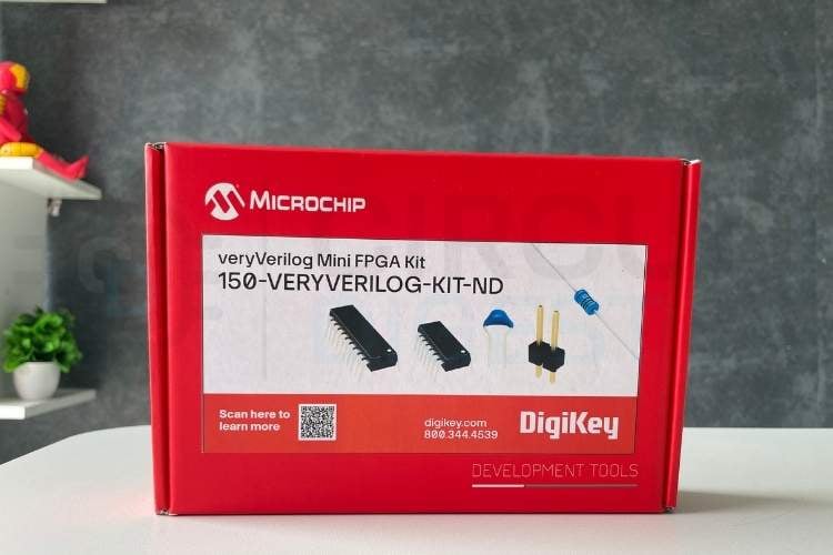
The board provides everything needed to begin experimenting with programmable logic. It includes user LEDs, push buttons, a USB interface for power and programming, and the necessary support circuitry around the target microcontroller. These onboard peripherals make it easy to implement and test digital logic circuits without requiring any additional hardware.
The heart of the veryVerilog Kit is the PIC16F13145, a member of Microchip's latest 8-bit PIC microcontroller family that integrates a powerful Configurable Logic Block. While the device functions as a fully featured microcontroller, the addition of the CLB allows developers to implement custom hardware logic alongside their firmware, bringing many FPGA design concepts into a familiar embedded development environment.
Microchip PIC16F13145 MCU
At first glance, the PIC16F13145 looks like any other member of Microchip's 8-bit PIC family. The PIC16F13145 combines a capable 8-bit CPU with 14 KB of Flash program memory and 1KB of RAM, with a clock of up to 32 MHz, providing ample resources for embedded control applications. It also integrates a wide range of digital and analog peripherals, including timers, PWM modules, communication interfaces, comparators, an ADC, and a DAC. Together with the CLB, these peripherals make the device suitable for applications ranging from sensor interfacing and motor control to custom digital logic and hardware acceleration.
One of the standout features of the PIC16F13145 is its Configurable Logic Block, which consists of 32 Basic Logic Elements (BLEs), each containing one 4-input LUT and one flip-flop. These programmable logic resources can be configured to implement custom combinational and sequential logic without consuming CPU cycles. The device also includes four Configurable Logic Cells (CLCs), which can be used independently or alongside the CLB to implement additional hardware-based logic functions. On the analog side, the PIC16F13145 features a 10-bit Analog-to-Digital Converter with Computation (ADCC) capable of sampling at up to 300 ksps, an 8-bit Digital-to-Analog Converter (DAC), and two high-speed comparators with response times as low as 50 ns. These peripherals enable efficient signal acquisition and analog processing without requiring additional external components. Apart from the other standard peripherals, the PIC16F13145 also features a Peripheral Pin Select (PPS), which allows many peripheral functions to be mapped to different I/O pins for greater design flexibility.
Microchip veryVerilog Kit Schematics
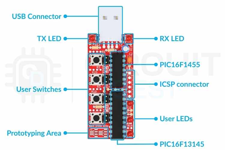
The complete schematic of the veryVerilog Kit is shown below. At the heart of the board is the PIC16F13145, which serves as the target microcontroller for implementing CLB based digital logic. An onboard PIC16F1455 functions as a USB programmer, communicating with the host computer over USB and programming the PIC16F13145 through the ICSP interface. The USB connector also powers the entire board, while an ICSP header is provided for users who wish to program or debug the target device using an external Microchip programmer.
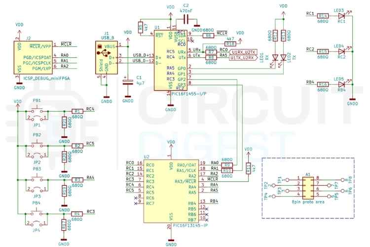
To make experimenting with digital logic easier, the board includes four push buttons connected to pins RC4, RC5, RA4, and RC3, respectively. The board also contains three user LEDs connected to RC1, RC2, and RB4, providing convenient visual outputs for CLB designs, alongside the two RX and TX LEDs that can be used to visualise the serial communication. An 8-pin prototype area provides an option to solder our own SOP8 or SOIC-8 chips to the board for prototyping. Apart from the programming circuitry and a few supporting components, such as the reset pull-up resistor and power supply decoupling capacitors, the hardware is very minimal and easy to build.
Assembling the veryVerilog Kit
Before getting started, you'll need to assemble the veryVerilog Kit. The kit uses only through-hole components, making it straightforward to solder using basic tools.
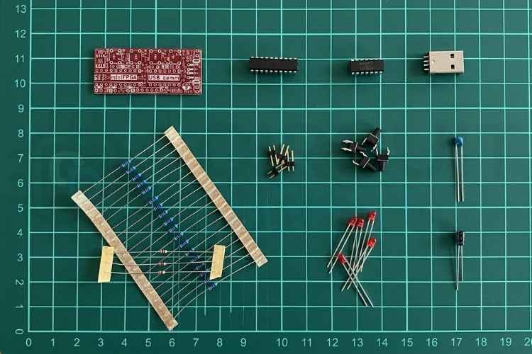
If you have assembled development kits before, the process should be familiar. New users can simply follow the official assembly guide, which includes the component placement, assembly sequence, and reference images for each step. Here is the fully assembled PCB with all the main components marked.
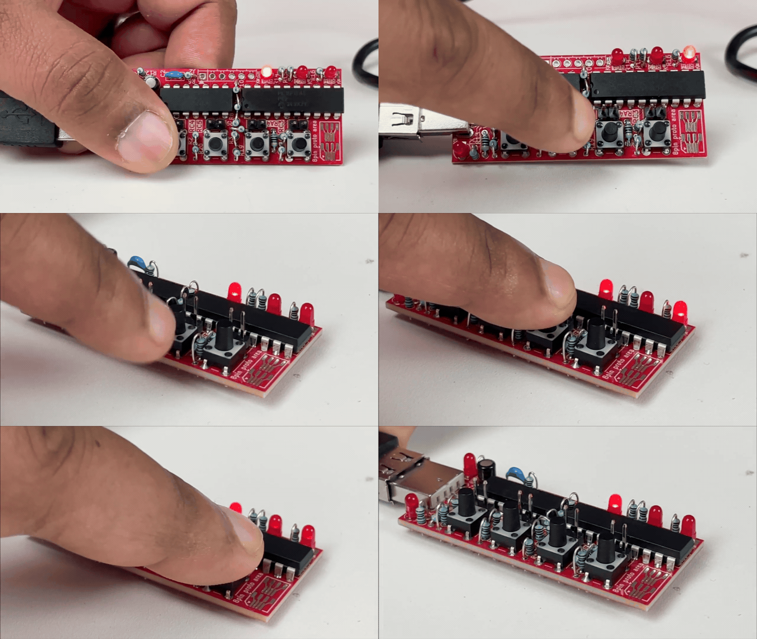
Once the assembly is complete, inspect the solder joints and verify that all components are installed in the correct orientation, particularly the LEDs, electrolytic capacitor, and the two DIP microcontrollers. After confirming there are no solder bridges or missing components, connect the board to your computer. The microcontroller comes preloaded with example code, which is an LED chaser. If everything was done right, the 3 user LEDs will start to flash in a pattern. The kit is now ready for software setup and programming.
Setting Up the Development Environment
With the hardware assembled, the next step is to set up the software development environment. Unlike traditional FPGA development, which often requires large synthesis tools and vendor-specific IDEs, for the veryVerilog Kit we will use the familiar Visual Studio Code IDE together with the MPLAB Extension Pack and XC8 Compiler. This combination allows you to configure the PIC16F13145, design digital logic graphically, generate the required firmware, and program the device from a single development environment.
How to Install the MPLAB XC8 C Compiler
The MPLAB XC8 C Compiler is Microchip’s compiler for developing applications for supported 8-bit PIC and AVR microcontrollers. To install it, download the appropriate XC8 package for your operating system from Microchip and launch the installer. The setup wizard will guide you through the installation, starting with the welcome screen and license agreement. Accept the license terms and continue to the Device Family Packs information page. Recent versions of XC8 no longer bundle device-specific header files, linker scripts, and startup files with the compiler; these are provided through DFPs and are automatically managed by the MPLAB extension pack for VS Code.
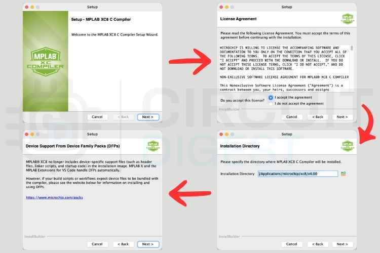
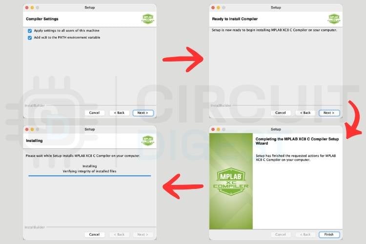
Continue through the installer, and on the installation directory selection page, keep the default location and continue. On the Compiler Settings screen, enable the option to add XC8 to the system PATH if you want to invoke the compiler directly from a terminal or command prompt. Proceed to the installation confirmation screen and start the installation. The installer will copy the compiler files and verify the installation before displaying the completion screen. Once finished, XC8 is ready to be selected as the compiler toolchain when creating or configuring a project in the MPLAB extension for VS Code. For more details about the setup, you can check out Microchip's Official training manual.
Install VS Code and MPLAB Extensions
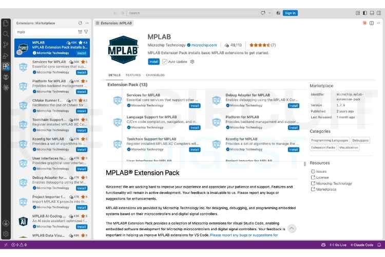
Begin by downloading and installing Visual Studio Code from the official Visual Studio Code website. The application is available for Windows, Linux, and macOS, so download the installer appropriate for your operating system and complete the standard installation process. Once VS Code is installed, launch the application and open the Extensions view from the Activity Bar. Search for MPLAB Extensions Pack and install the package published by Microchip. The extension pack provides the MPLAB development features required for creating and building the veryVerilog project, including the integration required for MPLAB Code Configurator.
Create New Project
After installing the extensions, create a new MPLAB project from within VS Code. From the menu bar, select View → Command Palette, then search for MPLAB: Create New Project and select the command. The MPLAB project wizard will open and ask for the project details. Enter a suitable project name and accept the default location, or choose a different directory if required. When the device selection screen appears, search for PIC16F13145 and select it as the target device. This is the microcontroller used by the veryVerilog kit. When prompted for the compiler, select XC8 and complete the project creation process.
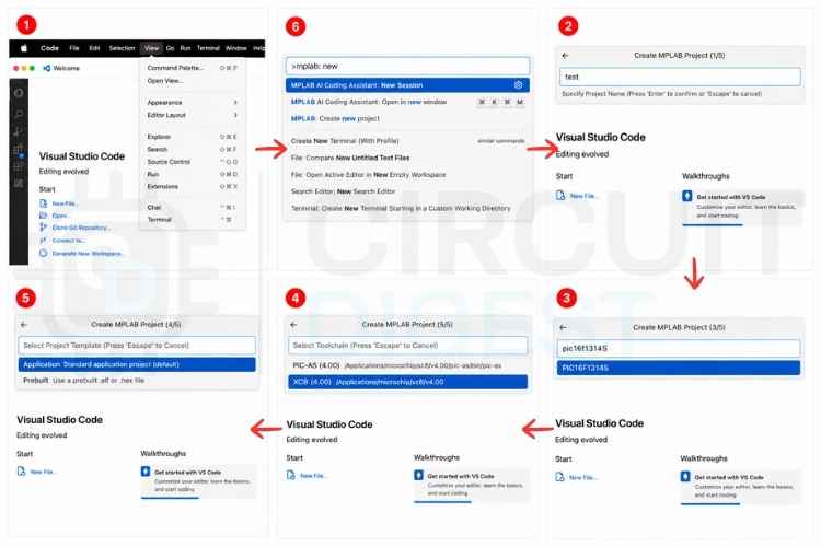
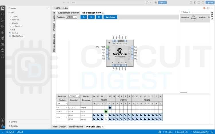
With the project created, the next step is to launch MPLAB Code Configurator. From the VS Code menu, select View → Command Palette, then search for MPLAB MCC: Launch and select it. MCC will open within the VS Code environment. If it's the first time you are opening the nMCC for a new project, select Create New MCC Config and associate the configuration with the project that was just created. Proceed with the default configuration options until the MCC graphical interface is displayed. Depending on the installation, VS Code may restart its extensions when the MCC configuration is first created. If MCC closes during this process, launch it again using View → Command Palette → MPLAB MCC: Launch.
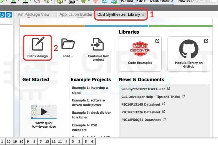
Once the MCC graphical interface is available, open the Device Resources section and locate the Libraries category. From the available libraries, select the CLB Synthesizer Library and add it to the project. The CLB Synthesizer is the part of the development environment used to create the configurable logic that will run inside the PIC16F13145. After adding the peripheral, select Blank Design to start with an empty CLB design.
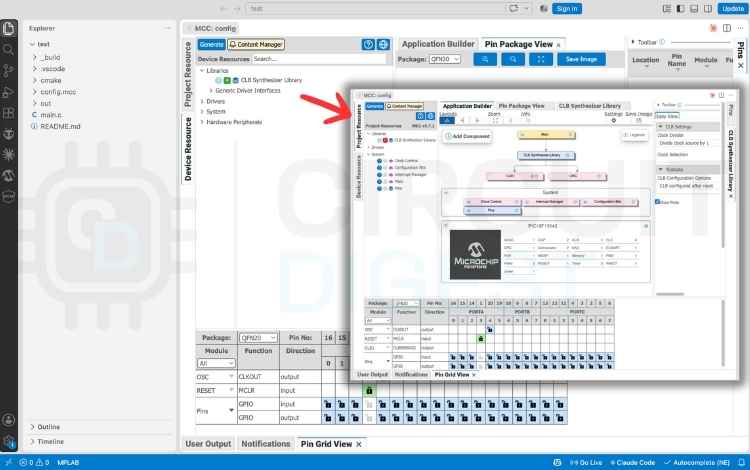
Although the CLB defaults to the HFINTOSC (32 MHz) clock source, Microchip recommends selecting LFINTOSC (31 kHz) when working through basic examples. The slower clock rate produces more stable and easier-to-follow output updates in the Try environment. This setting can be changed from the configuration panel on the right-hand side of the CLB Synthesizer.
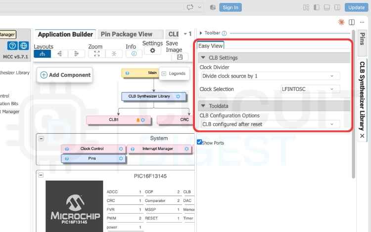
Once the CLB clock is set, we will create a new design by selecting the Black design in the CLB Synthesizer Library tab.
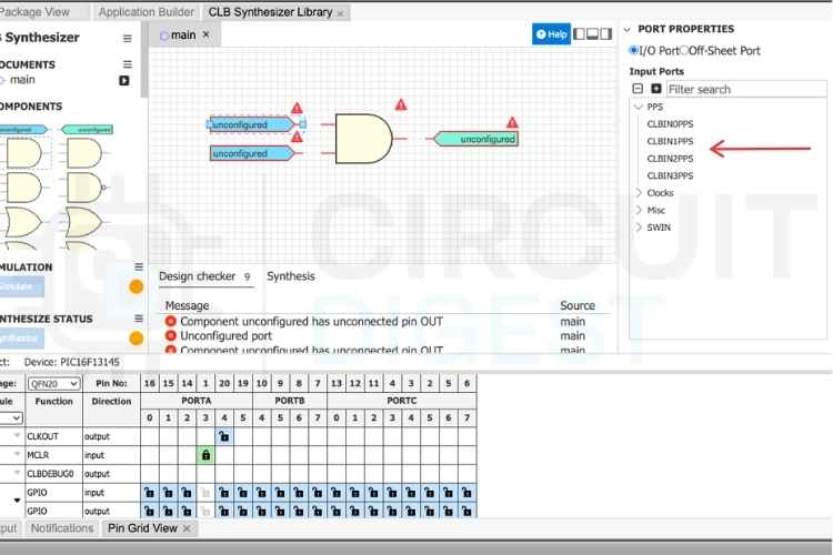
For this tutorial, we will create a simple AND gate using the CLB, which we will then use to control a user LED using two user-defined switches available on the veryVerilog PCB. For that, first drag two inputs and one output, along with an AND gate block, to the canvas. When you add these blocks to the canvas, they are unconfigured. To use them, we need to configure the inputs and outputs. For that, click on the unconfigured element, and the property panel will show the options to configure it. For the inputs, select CLBIN0PPS and CLBIN1PPS. For the output, select PPS_OUT0.
Once the input and output blocks are configured, connect them to the AND gate block. After all the blocks are connected, the result will look like the image below. As you may have observed, the Synthesize button on the left side of the canvas is also now enabled. Clicking the Synthesize button will synthesize the design and generate the code.
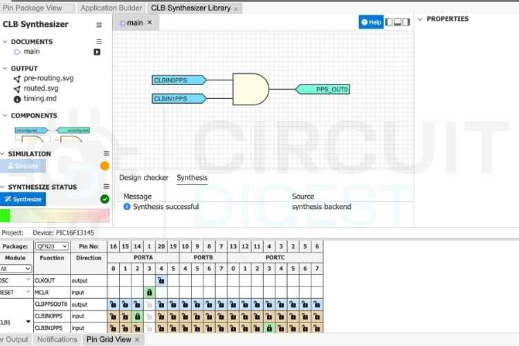
After generating the code, the total usage of the CLB will be shown as a bar graph under the Synthesize button. You might also notice that the pin grid view is updated. In the pin grid view, can assign the physical pins to the input and output blocks. For this example, we will use RC4 and RC5 as inputs and RC1 as output, since they are connected to the onboard switches and LED. To do so make a click on the lock icon on the pin grid array that corresponds to the correct pin. Make sure that the same pin is not assigned to different peripherals at the same time.
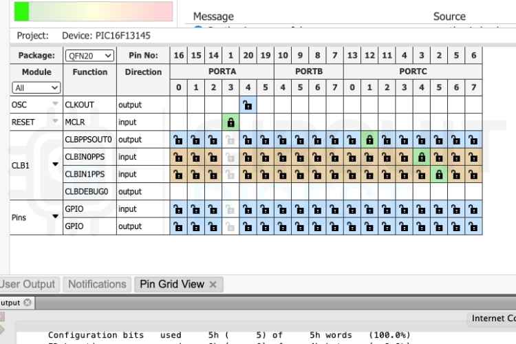
Compile the Design
With the CLB design synthesized and the pin assignments configured, the project can move to the code generation stage. In the MCC interface, select Generate Code. MCC will generate the source and configuration files required for the project based on the peripheral and CLB configuration. These generated files are added to the MPLAB project and are then used during the subsequent build process.
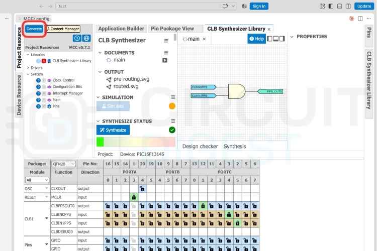
Build Design
After generating the project code, build the design using the MPLAB CMake build command. From the VS Code menu, select View → Command Palette, search for MPLAB CMake: Build, and select it. The build process uses the generated project files and the XC8 compiler to create the final firmware image. Once the build completes successfully, the required output files, including the HEX file used for programming, will be available in the project's build output directory.
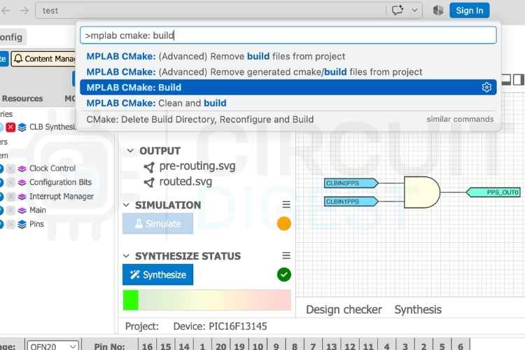
Once the build is successful, the HEX file will be created in the out folder.
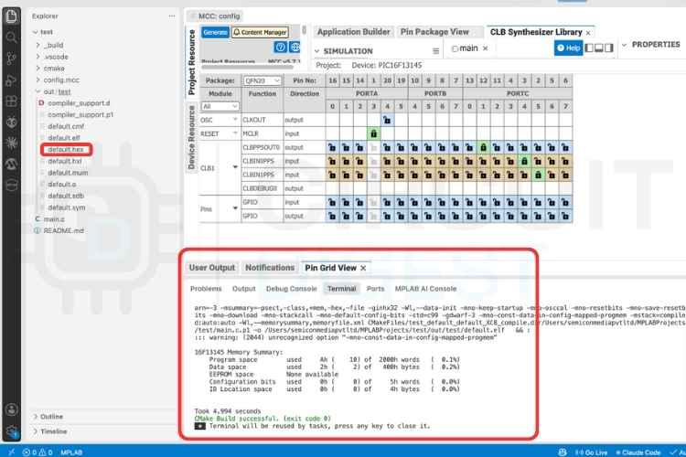
Flashing the Firmware to the veryVerilog Kit
Once the project has been compiled successfully, the generated HEX file needs to be programmed into the PIC16F13145 on the veryVerilog Kit. Unlike most microcontroller development boards, the veryVerilog Kit includes an onboard programmer and a browser-based programming interface, so no additional software is required for flashing the firmware.
Begin by connecting the veryVerilog Kit to your computer using a USB cable. Once connected, open the veryVerilog Web Programmer by navigating to the WEB ICSP Programmer tool page. Click the Connect to Programmer button and select the miniFPGA programmer from the list of available USB devices. If multiple programmers are connected to your computer, you can click Identify Programmer to blink the LEDs on the selected board for a few seconds, making it easy to identify the correct device. Once connected, the webpage will display information about the detected microcontroller along with the User ID of the firmware currently programmed on the device.
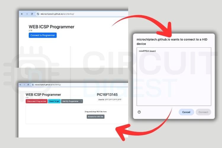
To program the board, simply drag and drop the generated HEX file onto the Drag and Drop area of the webpage. The programming process starts automatically and only takes a few seconds to complete. Alternatively, click the Browse for HEX File button and select the HEX file manually from your computer. Once programming is complete, the new firmware is immediately written to the PIC16F13145, and the board is ready to run your design. And here is the output. The LED will turn on only when we press both switches together.
Exploring the Demo Design
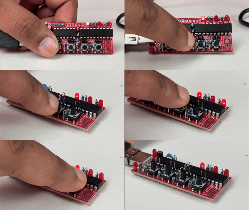
The factory-programmed firmware included with the veryVerilog Kit demonstrates how multiple hardware functions can be combined into a single CLB design. Rather than implementing a single logic circuit, it combines counters, logic gates, and PWM to create different LED patterns based on the state of the four onboard push buttons. Depending on which button is pressed, the LEDs can count in sequence, stop the counter, enable multiple counters simultaneously, illuminate at reduced brightness using PWM, or combine multiple functions.
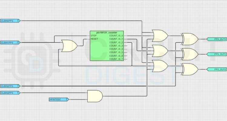
Each of the four onboard tactile switches modifies the behaviour differently. Pressing the RC4 switch overrides the counter and turns on all three LEDs simultaneously using OR logic. Pressing the RC5 switch pauses the running LED sequence and forces the first LED to remain ON. When the button is released, the counter resumes operation from where it stopped. The RA4 switch enables a second counter that is slightly phase-shifted from the first, creating a different LED pattern. Finally, pressing the RC3 switch uses PWM to dim all three LEDs, demonstrating how the CLB can work together with other peripherals to produce different output effects.
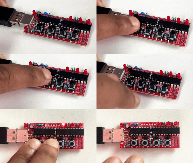
The demo also supports multiple button combinations. For example, pressing the RC5 and RC3 switches together keeps the first LED fully illuminated while dimming the other two LEDs using PWM. Pressing the RC4 and RA3 switches together disables all three LEDs. The complete source code and PCB design files can be found in the official veryVerilog GitHub repository.
Resources
This article covers the basics of using the veryVerilog Kit and the PIC16F13145 CLB. Once you're comfortable with these concepts, you can explore more digital logic examples and advanced designs using Microchip's online resources.
Logic Circuit Design 101 – An interactive course that introduces both basic and advanced digital logic concepts using the CLB.
Microchip veryVerilog Kit - Microchip veryVerilog Kit DigiKey product page.
These resources are a great way to continue learning and experimenting with the Configurable Logic Block beyond the examples covered in this article.

Add a comment
No account needed. Your comment appears once a moderator has reviewed it.