

Inverter circuits are often needed where it is not possible to get AC supply from the grid. An inverter circuit is used to convert DC power to AC power and it can be divided into two types that is Pure Sine Wave Inverters or Modified Square Wave Inverters. These pure sine wave inverters are very expensive, where the modified square wave inverters are inexpensive. Learn more about different types of inverter here.
In a previous article, I have shown you how not to make a modified square wave inverter by addressing the problems associated with it. So in this article, I will be making a simple pure sine wave inverter using Arduino, and explain the working principle of the circuit.
If you are making this circuit, please note that this circuit features no feedback, no overcurrent protection, no short circuit protection, and no temperature protection. Hence this circuit is built and demonstrated for educational purposes only, and it’s absolutely not recommended to build and use this type of circuit for commercial appliances. However you can add them to your circuit if required, the commonly used protection circuits like
Over Voltage Protection, Overcurrent Protection, Reverse polarity Protection, Short Circuit Protection, Hot Swap controller, etc. have already been discussed.
CAUTION: If you are making this type of circuit, please be extra careful about high voltage and voltage spikes generated by the switching signal to the input.
What is SPWM (Sinusoidal Pulse Width Modulation)?
As the name suggests, SPWM stands for Sinusoidal Pulse Width Modulation. As you may already know, a PWM signal is a signal in which we can change the frequency of the pulse as well as the on-time and off-time, which is also known as the duty cycle. If you want to learn more about PWM, you can read it here. So, by varying the duty cycle, we alter the average voltage of the pulse. The image below shows that-
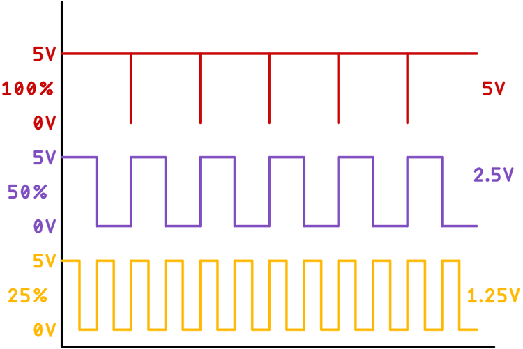
If we consider a PWM signal which is switching in between 0 - 5V which has a duty cycle of 100%, we will get an average output voltage of 5V, again if we consider the same signal with a duty cycle of 50%, we will get the output voltage of 2.5V, and for the duty cycle of 25%, it's half of that. That sums up the basic principle of the PWM signal, and we can move onto understanding the basic principle of the SPWM signal.
A sine voltage is primarily an analogy voltage which alters its magnitude over time, and we can reproduce this behaviour of a sine wave by continually changing the duty cycle of the PWM wave, the below image shows that.
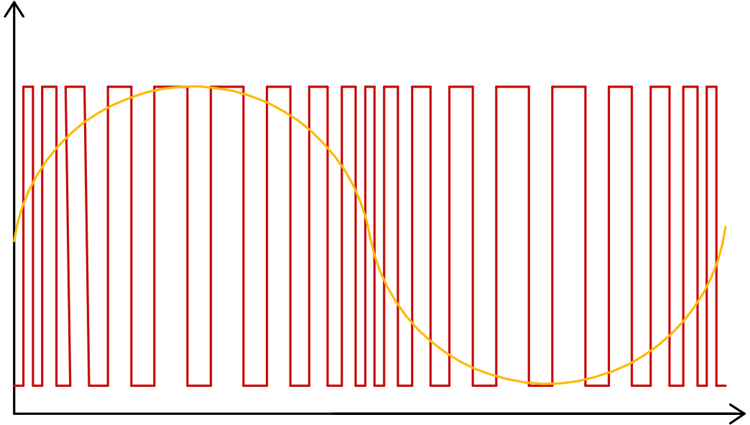
If you look at the schematic below, it will see there is a capacitor connected at the output of the transformer. This capacitor is responsible for smoothing out the AC signal from the carrier frequency.
The utilized input signal will charge and discharge the capacitor according to the input signal and load. As we have used a very high-frequency SPWM signal, it will have a very small duty cycle which is like 1%, this 1% duty cycle will charge the capacitor a little, the next duty cycle is 5%, this will again charge the capacitor a little more, following pulse will have a duty cycle of 10% and the capacitor will charge a little bit more, we will apply the signal until we have reached a duty cycle of 100% and from there, we will go back down to 1%. This will create a very smooth curve like a sine wave at the output. So, by providing proper values of the duty cycle at the input, we will have a very sinusoidal wave at the output.
How the SPWM Inverter Works
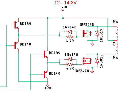
The above image shows the main driving section of the SPWM inverter, and as you can see, we have used two N-channel MOSFETs in half-bridge configuration to drive the transformer of this circuit, to reduce unwanted switching noise and to protect the MOSFET, we have used 1N5819 diodes parallel with the MOSFETs. To reduce any harmful spikes generated in the gate section, we have used the 4.7 ohms resistors parallel with 1N4148 diodes. Finally, the BD139 and BD 140 transistors are configured in a push-pull configuration to drive the gate of the MOSFET, because this MOSFET has a very high gate capacitance and requires a minimum of 10V at the base to turn on properly. Learn more about the working of Push-Pull amplifiers here.
To better understand the working principle of the circuit, we have reduced it to a point where this section of the MOSFET is ON. When the MOSFET is on the current, first flows through the transformer and then gets grounded by the MOSFET, thus a Magnetic flux will also be induced in the direction in which the current is flowing, and the core of the transformer will pass the magnetic flux in the secondary winding, and we will get the positive half cycle of the sinusoidal signal at the output.
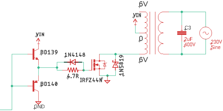
In the next cycle, the bottom part of the circuit is on the top part of the circuit is off that is why I have removed the top part, now the current flows in the opposite direction and generates a magnetic flux in that direction, thus reversing the direction of the magnetic flux in the core. Learn more about the working of MOSFET here.
Now, we all know that a transformer works by magnetic flux changes. So, turning both the MOSFETs on and off, one inverted to another and doing that 50 times in a second, will generate a nice oscillating magnetic flux inside the core of the transformer and the changing magnetic flux will induce a voltage in the secondary coil as we know by the faraday's law. That is how the basic inverter works.
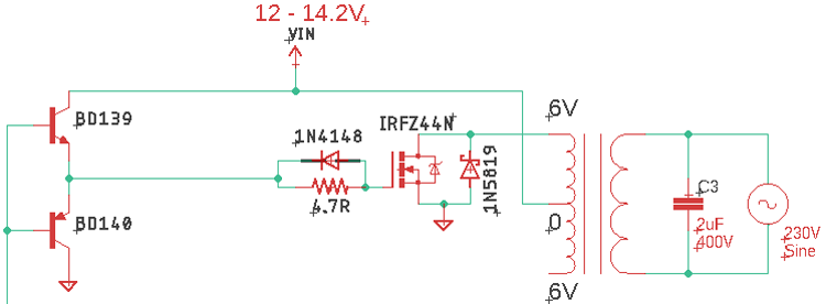
The complete SPWM inverter circuit used in this project is given below.

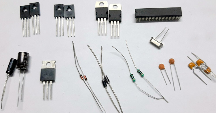
Components Required to Build SPWM Inverter
|
Sl.No |
Parts |
Type |
Quantity |
|
1 |
Atmega328P |
IC |
1 |
|
2 |
IRFZ44N |
Mosfet |
2 |
|
3 |
BD139 |
Transistor |
2 |
|
4 |
BD140 |
Transistor |
2 |
|
5 |
22pF |
Capacitor |
2 |
|
6 |
10K,1% |
Resistor |
1 |
|
7 |
16MHz |
Crystal |
1 |
|
8 |
0.1uF |
Capacitor |
3 |
|
9 |
4.7R |
Resistor |
2 |
|
10 |
1N4148 |
Diode |
2 |
|
11 |
LM7805 |
Voltage Regulator |
1 |
|
12 |
200uF,16V |
Capacitor |
1 |
|
13 |
47uF, 16V |
Capacitor |
1 |
|
14 |
2.2uF,400V |
Capacitor |
1 |
SPWM Inverter Circuit Construction
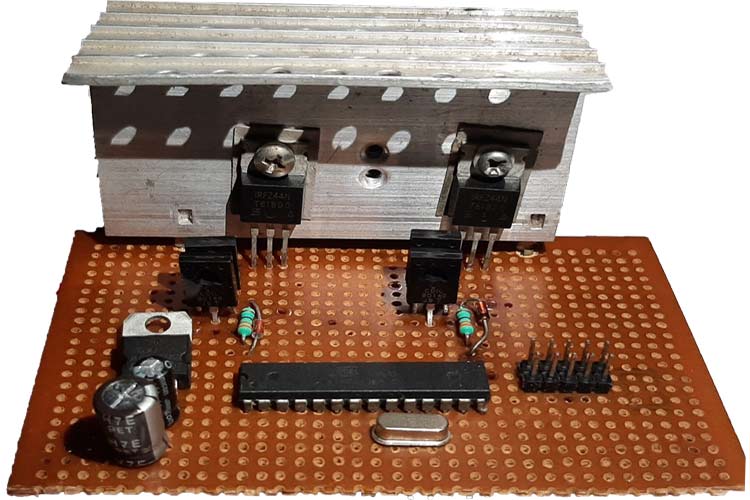
For this demonstration, the circuit is constructed on Veroboard, with the help of the schematic, At the output of the transformer, a huge amount of current will flow through the connection, so the connection jumpers need to be as thick as possible.
Arduino Program for SPWM Inverter
Before we go ahead and start to understand the code, let's clear out the basics. From the above working principle, you have learned how the PWM signal will look like at the output, now the question remains how we can make such a varying wave at the output pins of the Arduino.
To make the varying PWM signal, we are going to use the 16-bit timer1 with a prescaler setting of 1, which will give us 1600/16000000 = 0.1ms time for each count if we consider a single half-cycle of a sine wave, that fits exactly 100 times within a one-half cycle of the wave. In simple terms, we will be able to sample our sine wave 200 times.
Next, we have to divide our sine wave to 200 pieces and calculate their values with a correlation of the amplitude. Next, we have to convert those values to timer counter values by multiplying it with the counter limit. Finally, we have to put those values into a lookup table to feed it to the counter and we will get our sine wave.
To make things a little bit simpler, I am using a very well written SPWM code from GitHub which is made by Kurt Hutten.
The code is very simple, We begin our program by adding the required header files
#include <avr/io.h>
#include <avr/interrupt.h>
Next, we have our two lookup tables from which we are going to get the timer counter values.
int lookUp1[] = {50 ,100 ,151 ,201 ,250 ,300 ,349 ,398 ,446 ,494 ,542 ,589 ,635 ,681 ,726 ,771 ,814 ,857 ,899 ,940 ,981 ,1020 ,1058 ,1095 ,1131 ,1166 ,1200 ,1233 ,1264 ,1294 ,1323 ,1351 ,1377 ,1402 ,1426 ,1448 ,1468 ,1488 ,1505 ,1522 ,1536 ,1550 ,1561 ,1572 ,1580 ,1587 ,1593 ,1597 ,1599 ,1600 ,1599 ,1597 ,1593 ,1587 ,1580 ,1572 ,1561 ,1550 ,1536 ,1522 ,1505 ,1488 ,1468 ,1448 ,1426 ,1402 ,1377 ,1351 ,1323 ,1294 ,1264 ,1233 ,1200 ,1166 ,1131 ,1095 ,1058 ,1020 ,981 ,940 ,899 ,857 ,814 ,771 ,726 ,681 ,635 ,589 ,542 ,494 ,446 ,398 ,349 ,300 ,250 ,201 ,151 ,100 ,50 ,0 ,0 ,0 ,0 ,0 ,0 ,0 ,0 ,0 ,0 ,0 ,0 ,0 ,0 ,0 ,0 ,0 ,0 ,0 ,0 ,0 ,0 ,0 ,0 ,0 ,0 ,0 ,0 ,0 ,0 ,0 ,0 ,0 ,0 ,0 ,0 ,0 ,0 ,0 ,0 ,0 ,0 ,0 ,0 ,0 ,0 ,0 ,0 ,0 ,0 ,0 ,0 ,0 ,0 ,0 ,0 ,0 ,0 ,0 ,0 ,0 ,0 ,0 ,0 ,0 ,0 ,0 ,0 ,0 ,0 ,0 ,0 ,0 ,0 ,0 ,0 ,0 ,0 ,0 ,0 ,0 ,0 ,0 ,0 ,0 ,0 ,0 ,0 ,0 ,0 ,0 ,0 ,0 ,0 ,0 ,0 ,0 ,0 ,0 ,0 ,0};
int lookUp2[] = {0 ,0 ,0 ,0 ,0 ,0 ,0 ,0 ,0 ,0 ,0 ,0 ,0 ,0 ,0 ,0 ,0 ,0 ,0 ,0 ,0 ,0 ,0 ,0 ,0 ,0 ,0 ,0 ,0 ,0 ,0 ,0 ,0 ,0 ,0 ,0 ,0 ,0 ,0 ,0 ,0 ,0 ,0 ,0 ,0 ,0 ,0 ,0 ,0 ,0 ,0 ,0 ,0 ,0 ,0 ,0 ,0 ,0 ,0 ,0 ,0 ,0 ,0 ,0 ,0 ,0 ,0 ,0 ,0 ,0 ,0 ,0 ,0 ,0 ,0 ,0 ,0 ,0 ,0 ,0 ,0 ,0 ,0 ,0 ,0 ,0 ,0 ,0 ,0 ,0 ,0 ,0 ,0 ,0 ,0 ,0 ,0 ,0 ,0 ,0 ,50 ,100 ,151 ,201 ,250 ,300 ,349 ,398 ,446 ,494 ,542 ,589 ,635 ,681 ,726 ,771 ,814 ,857 ,899 ,940 ,981 ,1020 ,1058 ,1095 ,1131 ,1166 ,1200 ,1233 ,1264 ,1294 ,1323 ,1351 ,1377 ,1402 ,1426 ,1448 ,1468 ,1488 ,1505 ,1522 ,1536 ,1550 ,1561 ,1572 ,1580 ,1587 ,1593 ,1597 ,1599 ,1600 ,1599 ,1597 ,1593 ,1587 ,1580 ,1572 ,1561 ,1550 ,1536 ,1522 ,1505 ,1488 ,1468 ,1448 ,1426 ,1402 ,1377 ,1351 ,1323 ,1294 ,1264 ,1233 ,1200 ,1166 ,1131 ,1095 ,1058 ,1020 ,981 ,940 ,899 ,857 ,814 ,771 ,726 ,681 ,635 ,589 ,542 ,494 ,446 ,398 ,349 ,300 ,250 ,201 ,151 ,100 ,50 ,0};
Next, in the setup section, we initialize the timer counter control registers to be clear on each. For further information, you need to go through the datasheet of the atmega328 IC.
    TCCR1A = 0b10100010;
       /*10 clear on match, set at BOTTOM for compA.
         10 clear on match, set at BOTTOM for compB.
         00
         10 WGM1 1:0 for waveform 15.
       */
    TCCR1B = 0b00011001;
       /*000
         11 WGM1 3:2 for waveform 15.
         001 no prescale on the counter.
       */
    TIMSK1 = 0b00000001;
       /*0000000
         1 TOV1 Flag interrupt enable.
       */
After that, we initialize the input capture register with a predefined value of 16000 as this will help us to generate exactly 200 samples.
ICR1 = 1600; // Period for 16MHz crystal, for a switching frequency of 100KHz for 200 subdivisions per 50Hz sine wave cycle.
Next, we enable global interrupts by calling in the function,
sei();
Finally, we set Arduino pin 9 and 10 as output
DDRB = 0b00000110; // Set PB1 and PB2 as outputs.
That marks the end of the setup function.
The loop section of the code stays empty as it is a timer counter interrupt-driven program.
void loop(){; /*Do nothing . . . . forever!*/}
Next, we have defined the timer1 overflow vector, this interrupt function gets a call once the timer1 gets overflowed and generates an interrupt.
ISR(TIMER1_OVF_vect){
Next, we declare some local variables as static variables and we have started feeding the values to the capture and compare resistor.
static int num;
static char trig;
// change duty-cycle every period.
OCR1A = lookUp1[num];
OCR1B = lookUp2[num];
Finally, we pre-increment the counter to feed the next values to the capture and compare resistors, which marks the end of this code.
if(++num >= 200){ // Pre-increment num then check it's below 200.
       num = 0;       // Reset num.
       trig = trig^0b00000001;
       digitalWrite(13,trig);
     }
Testing the TL494 PWM Inverter Circuit
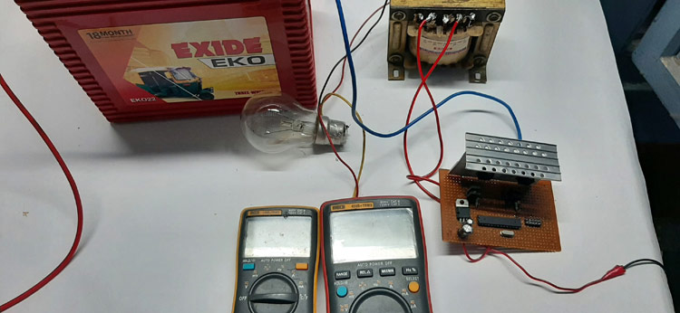
In order to test the circuit, the following setup is used.
- 12V lead-acid battery.
- A transformer which has a 6-0-6 tap and a 12-0-12 tap
- 100W incandescent light bulb as a load
- Meco 108B+TRMS Multimeter
- Meco 450B+TRMS Multimeter
Output Signal from Arduino:
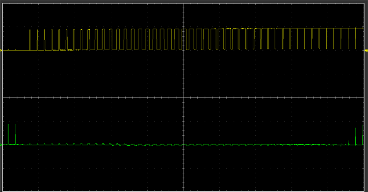
Once I have uploaded the code. I measured the output SPWM signal from the two pins of the Arduino which looks like the below image,
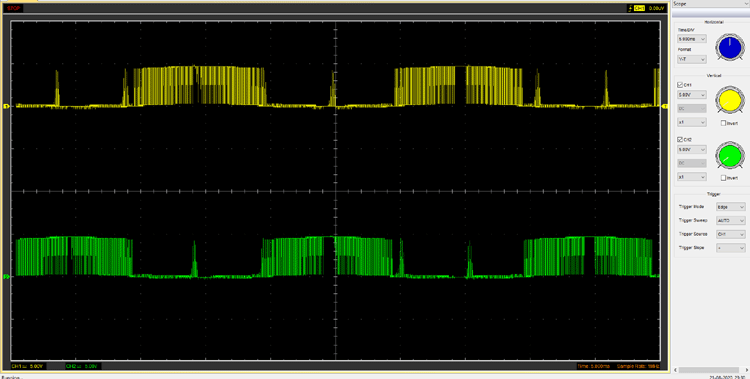
If we zoom in a little bit we can see the ever-changing duty cycle of the PWM wave.
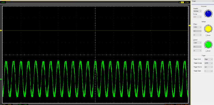
Next, the below image shows the output signal from the transformer.
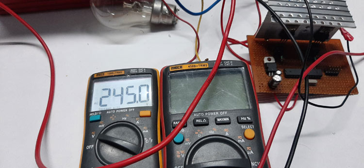
SPWM Inverter Circuit in Ideal state:
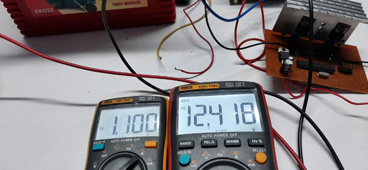
As you can see from the above image, this circuit draws around 13W while running ideal
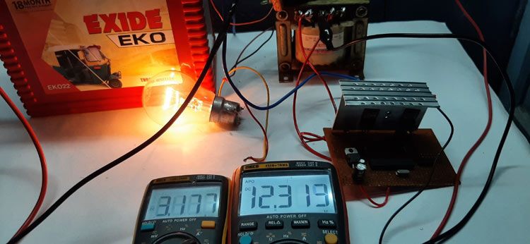
Output Voltage Without Load:
The output voltage of the inverter circuit is shown above, this is the voltage coming out at the output without any load attached.
Input Power Consumption:
The above image shows the input power which ic consume when a 40W load is attached.
Output Power Consumption:
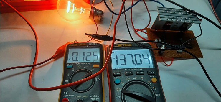
The above image shows the output power which is consumed by this circuit, (the load is a 40W incandescent light bulb)
With that, we conclude the testing part of the circuit. You can check out the video below for a demonstration. I hope you liked this article and learned a bit about SPWM and its implementation techniques. Keep reading, keep learning, keep building and I will see you in the next project.
Complete Project Code
/*
* sPWMv2.c
*
* Created: 31/12/2014 3:44:43 PM
*  Author: Kurt Hutten
SPWM on the atMega328 for the arduino Uno, might be compatible with other atmel chips / arduino boards.
Compare outputs A and B output to PORTB pins 1 and 2 which are pins 9 and 10 respectively on the Uno.
Also useful to know the led on the Uno is pin 5 on PORTB.
*/
#include <avr/io.h>
#include <avr/interrupt.h>
// Look up tables with 200 entries each, normalised to have max value of 1600 which is the period of the PWM loaded into register ICR1.
int lookUp1[] = {50 ,100 ,151 ,201 ,250 ,300 ,349 ,398 ,446 ,494 ,542 ,589 ,635 ,681 ,726 ,771 ,814 ,857 ,899 ,940 ,981 ,1020 ,1058 ,1095 ,1131 ,1166 ,1200 ,1233 ,1264 ,1294 ,1323 ,1351 ,1377 ,1402 ,1426 ,1448 ,1468 ,1488 ,1505 ,1522 ,1536 ,1550 ,1561 ,1572 ,1580 ,1587 ,1593 ,1597 ,1599 ,1600 ,1599 ,1597 ,1593 ,1587 ,1580 ,1572 ,1561 ,1550 ,1536 ,1522 ,1505 ,1488 ,1468 ,1448 ,1426 ,1402 ,1377 ,1351 ,1323 ,1294 ,1264 ,1233 ,1200 ,1166 ,1131 ,1095 ,1058 ,1020 ,981 ,940 ,899 ,857 ,814 ,771 ,726 ,681 ,635 ,589 ,542 ,494 ,446 ,398 ,349 ,300 ,250 ,201 ,151 ,100 ,50 ,0 ,0 ,0 ,0 ,0 ,0 ,0 ,0 ,0 ,0 ,0 ,0 ,0 ,0 ,0 ,0 ,0 ,0 ,0 ,0 ,0 ,0 ,0 ,0 ,0 ,0 ,0 ,0 ,0 ,0 ,0 ,0 ,0 ,0 ,0 ,0 ,0 ,0 ,0 ,0 ,0 ,0 ,0 ,0 ,0 ,0 ,0 ,0 ,0 ,0 ,0 ,0 ,0 ,0 ,0 ,0 ,0 ,0 ,0 ,0 ,0 ,0 ,0 ,0 ,0 ,0 ,0 ,0 ,0 ,0 ,0 ,0 ,0 ,0 ,0 ,0 ,0 ,0 ,0 ,0 ,0 ,0 ,0 ,0 ,0 ,0 ,0 ,0 ,0 ,0 ,0 ,0 ,0 ,0 ,0 ,0 ,0 ,0 ,0 ,0 ,0};
int lookUp2[] = {0 ,0 ,0 ,0 ,0 ,0 ,0 ,0 ,0 ,0 ,0 ,0 ,0 ,0 ,0 ,0 ,0 ,0 ,0 ,0 ,0 ,0 ,0 ,0 ,0 ,0 ,0 ,0 ,0 ,0 ,0 ,0 ,0 ,0 ,0 ,0 ,0 ,0 ,0 ,0 ,0 ,0 ,0 ,0 ,0 ,0 ,0 ,0 ,0 ,0 ,0 ,0 ,0 ,0 ,0 ,0 ,0 ,0 ,0 ,0 ,0 ,0 ,0 ,0 ,0 ,0 ,0 ,0 ,0 ,0 ,0 ,0 ,0 ,0 ,0 ,0 ,0 ,0 ,0 ,0 ,0 ,0 ,0 ,0 ,0 ,0 ,0 ,0 ,0 ,0 ,0 ,0 ,0 ,0 ,0 ,0 ,0 ,0 ,0 ,0 ,50 ,100 ,151 ,201 ,250 ,300 ,349 ,398 ,446 ,494 ,542 ,589 ,635 ,681 ,726 ,771 ,814 ,857 ,899 ,940 ,981 ,1020 ,1058 ,1095 ,1131 ,1166 ,1200 ,1233 ,1264 ,1294 ,1323 ,1351 ,1377 ,1402 ,1426 ,1448 ,1468 ,1488 ,1505 ,1522 ,1536 ,1550 ,1561 ,1572 ,1580 ,1587 ,1593 ,1597 ,1599 ,1600 ,1599 ,1597 ,1593 ,1587 ,1580 ,1572 ,1561 ,1550 ,1536 ,1522 ,1505 ,1488 ,1468 ,1448 ,1426 ,1402 ,1377 ,1351 ,1323 ,1294 ,1264 ,1233 ,1200 ,1166 ,1131 ,1095 ,1058 ,1020 ,981 ,940 ,899 ,857 ,814 ,771 ,726 ,681 ,635 ,589 ,542 ,494 ,446 ,398 ,349 ,300 ,250 ,201 ,151 ,100 ,50 ,0};
void setup(){
    // Register initialization, see datasheet for more detail.
    TCCR1A = 0b10100010;
       /*10 clear on match, set at BOTTOM for compA.
         10 clear on match, set at BOTTOM for compB.
         00
         10 WGM1 1:0 for waveform 15.
       */
    TCCR1B = 0b00011001;
       /*000
         11 WGM1 3:2 for waveform 15.
         001 no prescale on the counter.
       */
    TIMSK1 = 0b00000001;
       /*0000000
         1 TOV1 Flag interrupt enable.
       */
    ICR1   = 1600;     // Period for 16MHz crystal, for a switching frequency of 100KHz for 200 subdivisions per 50Hz sine wave cycle.
    sei();             // Enable global interrupts.
    DDRB = 0b00000110; // Set PB1 and PB2 as outputs.
    pinMode(13,OUTPUT);
}
void loop(){; /*Do nothing . . . . forever!*/}
ISR(TIMER1_OVF_vect){
    static int num;
    static char trig;
    // change duty-cycle every period.
    OCR1A = lookUp1[num];
    OCR1B = lookUp2[num];
    if(++num >= 200){ // Pre-increment num then check it's below 200.
       num = 0;       // Reset num.
       trig = trig^0b00000001;
       digitalWrite(13,trig);
     }
}Comments
In Electronics, there is always a way out. There will be a voltage amplification. The signals at the output delvers when the right transformer is used.
best
Como fazer para 60hz? parabéns

Hello,
You write that we need the push-pull stage to get at least 10V at the gate of the mosfet to turn on properly.
But you drive the push-pull bases with a 5V signal from the arduino. The npn-transistor will not conduct if the emitter voltage gets above ~ base voltage - 0.6V. Thus the output of the push-pull stage will never be higher than 4.4V.
The only thing we get here is a current amplification.