

Switched-mode power supply circuits (SMPS) are most often required in many electronic designs to convert the AC mains voltage to a suitable level of DC voltage for the device to operate. This type of AC-DC converter takes in the 230V/110V AC mains voltage as input and converts it to low-level DC voltage by switching it, hence the name switch-mode power supply. We have already built a few SMPS circuits earlier, like this 5V 2A SMPS circuit and 12V 1A TNY268 SMPS circuit. We even build our own SMPS transformer that could be used in our SMPS designs along with the driver IC. In this project, we will build another 12V 1A SMPS circuit using the VIPer22A, which is a popular low-cost SMPS driver IC from STMicroelectronics. This tutorial will take you through the complete circuit and will also explain how to build your own transformer for the VIPER circuit. Interesting, right? Let’s get started. This article is a complete guide to the VIPer22A power supply circuit design. A high-quality, low-cost solution for the design of a reliable 12V 1A SMPS. We will cover the complete VIPer22A circuit diagram, IC pinout, custom transformer construction, testing of the switch-mode power supply, etc., to assist you in building your own switch-mode power supply.
Table of Contents
VIPer22A Power Supply Design Specifications
Same as like previous SMPS-based projects, different kinds of power supplies work in different environments and work in a specific input-output boundary. This SMPS also has a specification. Therefore, proper specification analysis needs to be done before proceeding with the actual design.
Input specification: This will be an SMPS in the AC to DC conversion domain. Therefore, the input will be AC. In this project, the input voltage is fixed. It is as per the European standard voltage rating. So, the input AC voltage of this SMPS will be 220-240VAC. It is also the standard voltage rating of India.
Output specification: The output voltage is selected as 12V with a 1A current rating. Thus, it will be a 12W output. Since this SMPS will provide a constant voltage irrespective of the load current, it will work in CV (Constant Voltage) mode. Also, the output voltage will be constant and steady at the lowest input voltage with maximum load (2A) across the output.
Output ripple voltage: It is highly desired that a good power supply has a ripple voltage of less than 30mV pk-pk. The targeted ripple voltage is the same for this SMPS, with less than 30mV pk-pk ripple. However, SMPS output ripple is highly dependent on the SMPS construction, the PCB and the type of capacitor used. We used a low ESR capacitor of 105-degree rating from Wurth Electronics, and the expected output ripple seems to be below.
Protection circuits: There are various protection circuits that can be employed in an SMPS for a safe and reliable operation. The protection circuit protects the SMPS as well as the associated load. Depending on the type, the protection circuit can be connected across the input or across the output. For this SMPS, input surge protection will be used with a maximum operating input Voltage of 275VAC. Also, to deal with EMI issues, a common-mode filter will be used to blank out the generated EMI. On the Output side, we will include short-circuit protection, over-voltage protection, and over-current protection.
| Parameter | Specification | Description |
| Input Voltage Range | 85-265 VAC | Universal AC input (European/US standard) |
| Output Power | Up to 20W | Open-frame configuration |
| Output Voltage | 12V DC | Regulated constant voltage |
| Output Current | 1A (continuous) | 12W total output power |
| Switching Frequency | 60 kHz (typical) | Variable frequency operation |
| Efficiency | ~75-80% | At full load conditions |
| Operating Temperature | -40°C to +150°C | Junction temperature |
| Protection Features | OVP, OCP, OTP | Multiple built-in protections |
Selection of the SMPS Driver IC
Every SMPS circuit requires a Power Management IC, also known as a switching IC or SMPS IC or Drier IC. Let’s sum up the design considerations to select the ideal Power Management IC that will be suitable for our design. Our Design requirements are
- 12W output. 12V 1A at full load.
- European Standard input rating. 85-265VAC at 50Hz
- Input surge protection. Maximum input voltage 275VAC.
- Output short circuit, over-voltage and over-current protection.
- Constant voltage operations.
From the above requirements, there is a wide range of ICs to select from, but for this project, we have selected the VIPer22A power driver from STMicroelectronics. It is a very low-cost power driver IC from STMicroelectronics.
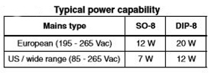
In the above image, the typical power rating of VIPer22A IC is shown. However, there is no specified section for open-frame or adapter-type power output specification. We will make the SMPS in an open frame for the European input rating.
VIPer22A IC Pinout Configuration
In such a segment, VIPer22A could provide 20W output. We will use it for a 12W output. The VIPer22A IC pinout features an 8-pin DIP package with the following configuration:
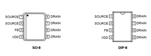
| Pin Number | Pin Name | Function |
| 1, 2, 3 | DRAIN | Internal MOSFET drain connection (connect to transformer primary) |
| 4 | SOURCE | Internal MOSFET source and power ground |
| 5 | FB | Feedback pin for output voltage regulation (via optocoupler) |
| 6 | CONTROL | Soft-start and control functions |
| 7 | VDD | Supply voltage for internal circuitry (bias winding) |
| 8 | SOURCE | Additional source pin for thermal management |
Complete VIPer22A Circuit Diagram and Schematic Analysis
The best way to build the circuit is by using Power Supply Design software. You can download the VIPer Design Software Version 2.24 to use VIPer22A; the latest version of this software no longer supports VIPer22A. It is excellent power supply design software from STMicroelectronics. By providing the design requirement info, the complete power supply circuit diagram can be generated. The VIPer22A circuit for this project, generated by the software, is shown below. The VIPer22A circuit diagram implements a flyback converter topology with galvanic isolation. This VIPer22A schematic can be generated using STMicroelectronics' VIPer Design Software for precise component calculations.
The VIPer22A IC from STMicroelectronics is an integrated power conversion solution for a flyback converter topology. This SMPS driver IC combines a PWM controller and a high-voltage integrated 730V MOSFET, eliminating external components to lower total system costs.

Before going straight into building the prototype part, let's explore the circuitry operation. The VIPer22A SMPS circuit consists of ten critical sections working together for efficient AC-DC conversion:
- Input surge and SMPS fault protection
- Input Filter
- AC-DC conversion
- Driver circuitry or switching circuit
- Clamp circuit.
- Magnetics and galvanic isolation.
- EMI filter
- Secondary Rectifier
- Filter Section
- Feedback section.
Input Protection and Filtering (Primary Side)
Input surge and SMPS fault protection.
This section consists of two components, F1 and RV1. F1 is a 1A 250VAC slow blow fuse, and RV1 is a 7mm 275V MOV (Metal Oxide Varistor). During a high voltage surge (more than 275VAC), the MOV became dead short and blew the input Fuse. However, due to the slow-blow feature, the fuse withstands inrush current through the SMPS.
Input Filter
The capacitor C3 is a 250VAC line filter capacitor. It is an X-type capacitor similar to the one that we used in our transformer less power supply circuit design.
AC-DC conversion.
The AC-DC conversion is done using a DB107 full bridge rectifier diode. It is a 1000V 1A-rated rectifier diode. The filtering is done using the 22uF 400V capacitor. However, during this prototype, we used a very large value of a capacitor. Instead of 22uF, we used an 82uF capacitor due to the availability of the capacitor. Such a high-value capacitor is not required for the operation of the circuit. 22uF 400V is sufficient for 12W output rating.
Driver circuitry or switching circuit.
VIPer22A requires power from the bias winding of the transformer. After getting the bias voltage, VIPer starts switching across the transformer using an in-built high voltage MOSFET. D3 is used for converting the AC bias output to a DC, and the R1, 10 Ohm resistor is used for controlling the inrush current. The filter capacitor is a 4.7uF 50V for smoothing out the DC ripple.
Clamp Circuit for Voltage Spike Suppression
The transformer acts as a huge inductor across the power driver IC VIPer22. Therefore, during the switching off-cycle, the transformer creates high voltage spikes due to the leakage inductance of the transformer. These high-frequency voltage spikes are harmful to the power driver IC and can cause failure of the switching circuit. Thus, this needs to be suppressed by the diode clamp across the transformer. D1 and D2 are used for the clamp circuit. D1 is the TVS diode, and D2 is an ultra-fast recovery diode. D1 is used for clamping the voltage, whereas D2 is used as a blocking diode. As per the design, the targeted clamping voltage (VCLAMP) is 200V. Therefore, P6KE200A is selected, and for ultra-fast blocking-related issues, UF4007 is selected as D2.
Magnetics and galvanic isolation.
The transformer is a ferromagnetic transformer, and it not only converts the high voltage AC to a low voltage AC but also provides galvanic isolation. It has three winding orders. Primary, Auxiliary or Bias winding and the Secondary winding.
EMI filter.
EMI filtering is done by the C4 capacitor. It increases the immunity of the circuit to reduce the high EMI interference. It is a Y-Class capacitor with a voltage rating of 2kV.
Secondary Side Rectification and Filtering
The output from the transformer is rectified and converted to DC using D6, a Schottky rectifier diode. As the output current is 2A, a 3A 60V diode is selected for this purpose. SB360 is a 3A 60V-rated Schottky diode.
Filter Section.
C6 is the filter capacitor. It is a Low ESR capacitor for better ripple rejection. Also, an LC post-filter is used, where L2 and C7 provide better ripple rejection across the output.
Feedback section.
The output voltage is sensed by the U3 TL431 and R6 and R7. After sensing the line, U2, the Optocoupler is controlled and galvanically isolates the secondary feedback sensing portion from the primary side controller. The PC817 is an Optocoupler. It has two sides: a transistor and an LED inside it. By controlling the LED, the transistor is controlled. Since the communication is done optically, it has no direct electrical connection, therefore satisfying the galvanic isolation on the feedback circuit too.
Now, as the LED directly controls the transistor, by providing sufficient bias across the Optocoupler LED, one can control the Optocoupler transistor, more specifically driver circuit. This control system is employed by the TL431. A shunt regulator. As the shunt regulator has a resistor divider across it reference pin, it can control the Optocoupler LED, which is connected across it. The feedback pin has a reference voltage of 2.5V. Therefore, the TL431 can be active only if the voltage across the divider is sufficient. In our case, the voltage divider is set to a value of 5V. Therefore, when the output reaches 5V, the TL431 gets 2.5V across the reference pin and thus activates the Optocoupler's LED, which controls the transistor of the Optocoupler and indirectly controls the TNY268PN. If the voltage is not sufficient across the output, the switching cycle is immediately suspended.
First, the TNY268PN activates the first cycle of switching and then senses its EN pin. If everything is alright, it will continue the switching; if not, it will try once again after some time. This loop continued until everything got normal, thus preventing short circuit or overvoltage issues. This is why it is called flyback topology, as the output voltage is flown back to the driver for sensing-related operations. Also, the trying loop is called a hiccup mode of operation on the failure condition.
Building the Custom SMPS Transformer
Let's see the generated transformer construction diagram. This diagram is obtained from the power supply design software that we discussed earlier.
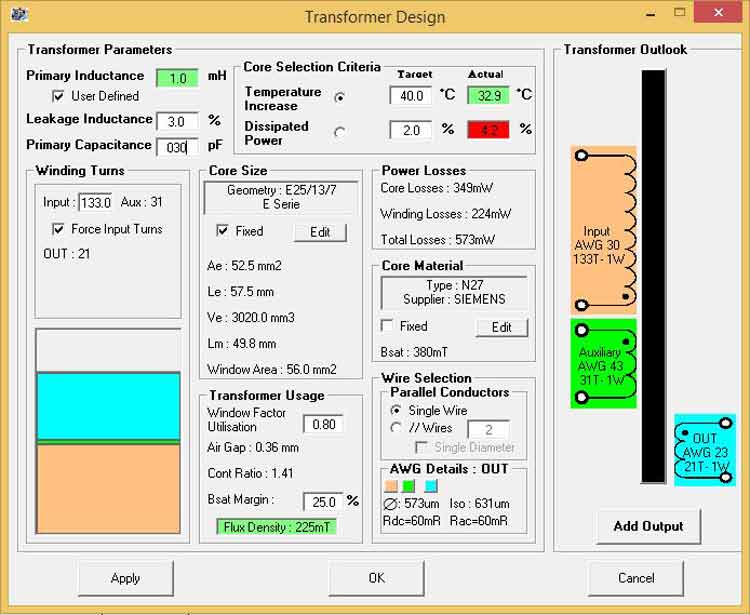
The Core is E25/13/7 with an air gap of 0.36mm. The primary inductance is 1mH. For the construction of this transformer, the following things are needed. If you are new to transformer construction, please read the article on how to build your own SMPS transformer.
- Polyester Tape
- E25/13/7 Core pairs with 0.36mm air gap.
- 30 AWG copper wire
- 43 AWG copper wire (We used 36 AWG due to unavailability)
- 23 AWG (We used 36 AWG, too, for this one)
- Horizontal or Vertical Bobbin (We used a Horizontal Bobbin)
- A Pen for holding the Bobbin during winding.
Transformer Winding Procedure
Step 1: Hold the Core using a pen, start 30 AWG copper wire from pin 3 of the bobbin and continue 133 turns clockwise to pin 1. Apply 3 layers of polyester tape.
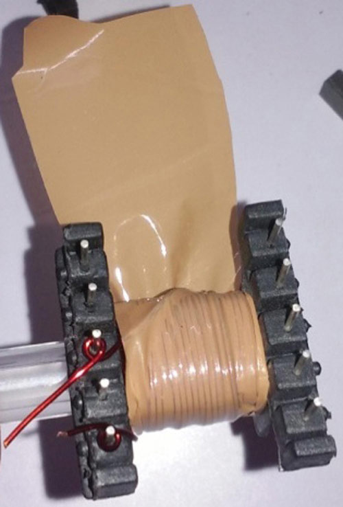
Auxiliary Bias Winding (Pin 4 to Pin 5)
Step 2: Start the Bias winding using 43 AWG copper wire from pin 4 and continue to the 31 turns, and end the winding at pin 5. Apply 3 layers of polyester tape.
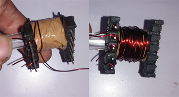
Start the Bias winding using 43 AWG copper wire from pin 4 and continue to the 31 turns, and end the winding at pin 5. Apply 3 layers of polyester tape.
Secondary Output Winding (Pin 10 to Pin 9)
Step 3: Start the secondary winding from pin 10 and continue clockwise winding of 21 Turns. Apply 4 layers of polyester tape.
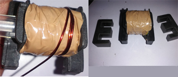
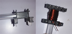
Core Assembly and Vibration Damping
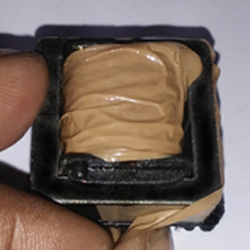
Step 4: Secure the gapped core with the duct tape, wrapping side by side. This will reduce the vibration during high-density flux transfer.
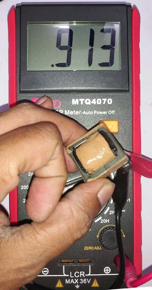
Once the build is done, the transformer is tested with an LCR meter to measure the inductance value of the coils. The meter is showing 913 mH, which is close to the 1mH primary inductance.
PCB Assembly and Construction Tips
Building the VIPer22A circuit on a PCB or perfboard requires attention to layout, creepage distances, and thermal management for reliable long-term operation.
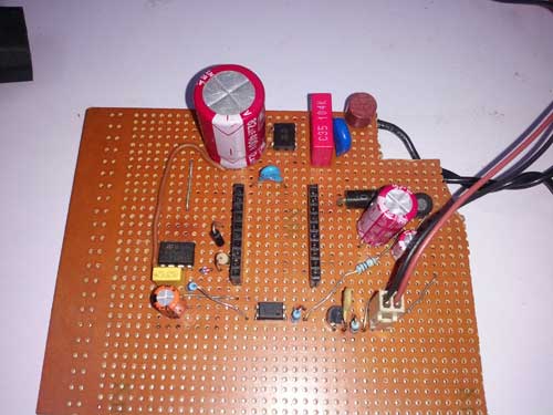
With the rating of the transformer verified, we can proceed with soldering all the components on a Vero board as given in the circuit diagram. My board, once the soldering job was done, looked like this:

Testing the VIPer22A 12V 1A Power Supply
To test the circuit, I connected the input side to the mains power supply through a VARIAC to control the input AC mains voltage. In the image below, the output voltage at 225VAC is shown.
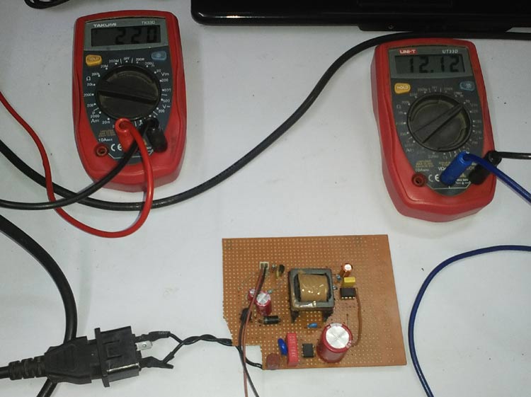
As you can see on the output side, we get 12.12V, which is close to the desired 12V output voltage. The complete working is shown in the video attached at the bottom of this page. Hope you understood the tutorial and learnt how to build your own SMPS circuits with a handmade transformer. If you have any questions, leave them in the comment section below.
Troubleshooting Common Issues
| Problem | Possible Cause | Solution |
| No Output Voltage | Incorrect transformer phasing or open bias winding | Verify transformer pin connections and bias winding continuity |
| Low Output Voltage | Insufficient turns ratio or feedback calibration | Check R6/R7 divider values, adjust for 2.5V at TL431 reference |
| High Ripple Voltage | Poor filtering or ESR in output capacitors | Replace with low-ESR capacitors rated 105°C, add LC post-filter |
| Audible Noise | Transformer vibration or loose core | Secure core with additional duct tape, verify air gap alignment |
| IC Overheating | Excessive load current or poor clamp circuit | Verify clamp components, reduce load, add heatsinking to IC |
| Intermittent Operation | Feedback instability or marginal bias supply | Check optocoupler orientation, increase bias winding filter capacitor |
Comparison: VIPer22A vs Alternative SMPS ICs
Parameter | VIPer22A | TNY268PN | LNK306 |
|---|---|---|---|
Manufacturer | STMicroelectronics | Power Integrations | Power Integrations |
Power Output | Up to 20W | Up to 18W | Up to 7W |
Package Type | 8-pin DIP | 8-pin DIP | 8-pin DIP |
Integrated MOSFET | 730V | 700V | 700V |
Switching Frequency | 60 kHz (typical) | 132 kHz | 66 kHz |
Feedback Method | Optocoupler required | Optocoupler required | Optocoupler required |
Typical Efficiency | 75-80% | 78-82% | 73-78% |
Cost (Relative) | Low ($) | Medium ($) | Low ($) |
Best Application | 12V/24V medium power | 5V/12V adapters | 5V low power supplies |
This detailed guide walks through the entire design, build, and testing of a VIPer22A power supply circuit with an output of 12V at 1A. The VIPer22A switched-mode power supply (SMPS) circuit presents a great balance of performance, cost, and simplicity for any low-powered AC-DC conversion application. The VIPer22A circuit diagram and VIPer22A schematic shown are a reliable flyback converter design compatible with many applications.
Our experts focus on creating practical, hands-on tutorials that help makers and engineers master Raspberry Pi projects, Arduino, Electronic Circuits, Power Supply Circuits and IoT development projects.
I hope you liked this article and learned something new from it. If you have any doubts, you can ask in the comments below or use our forum for a detailed discussion.
Ready to build your own VIPer22A power supply? Start with careful component selection, take time to properly wind the transformer following the specifications provided, and always test gradually using proper safety equipment.
Frequently Asked Questions About the Viper22a Circuit
⇥ Q1: What is the highest output power rating of VIPer22A IC?
VIPer22A is capable of providing up to 20W in open-frame applications for universal AC input (85-265VAC). For closed adapter designs, the highest power is reduced to about 13W due to thermal limitations. Our 12W solution falls within very safe thermal margins.
⇥ Q2: Is it possible to use VIPer22A for 5V power supply applications?
Yes, VIPer22A performs very well on 5V outputs. Just adjust the secondary turns of the transformer (raise to around 35 turns on 5V) and modify the feedback resistor divider (R6/R7) to bring the TL431 reference to 2.5V with 5V output voltage.
⇥ Q3: Why is there no output voltage on my VIPer22A circuit?
Most frequent reasons are reverse bias winding dot phasing (incorrect transformer winding phasing), open bias winding connection, or a shorted output that inhibits startup. Check the bias winding supplies 12-18V DC to the VDD pin under working conditions. Transformer continuity and right pin connections check.
⇥ Q4: What is the purpose of the air gap in the transformer core of VIPer22A?
The air gap of 0.36mm helps to prevent the core from saturating during the switching by ensuring the primary inductance is a nominal 1mH. If the air gap is not effective, high current saturates the ferrite core, which can lead to high losses, overheating, a general reduction in efficiency and ultimately cause VIPer22A to fail due to overcurrent.
⇥ Q5: Can VIPer22A operate without opting for isolation with the feedback from an optocoupler?
No, VIPer22A requires feedback to regulate voltage to operate. Output voltage is uncontrolled without an optocoupler (PC817) and TL431 feedback network, and can even exceed safe voltage levels. The IC is dependent on the feedback (FB) pin signal to adjust the duty cycle and provide a 12V fixed output in response to changing load conditions.
⇥ Q6: How do I minimise the output ripple voltage in the VIPer22A power supply?
Utilise low-ESR output capacitors rated 105°C (Recommended by Wurth Electronics), use an LC post-filter (ferrite bead inductor with ceramic capacitor), have good PCB layout with short traces, include parallel ceramic capacitors (100nF) in parallel across the electrolytic bulk capacitor, and check that the Schottky diode has a low reverse recovery time.
⇥ Q7: Which protection features does VIPer22A SMPS circuit possess?
VIPer22A circuit offers integrated protection: input surge protection through 275V MOV, overcurrent protection through slow-blow fuse, short-circuit protection with hiccup mode operation, overvoltage protection through TL431 feedback regulation, and thermal shutdown within the IC. Voltage spike is protected against by a TVS clamp diode.
Projects using Power Supply Circuit
Previously, we have used this power supply circuit to build many interesting projects. If you want to know more about those topics, links are given below.

+5V and --5V Dual Power Supply Circuit
So in this tutorial, we will learn how to build a simple low-current dual 5V Power Supply Circuit that can be powered from our USB ports. Similarly, we have previously built a +12V and -12V Dual Power Supply Circuit.

+12V and -12V Dual Power Supply Circuit
The objective of this project is to convert a 220V AC supply into to +12V and -12v DC supply, which is why it is named Dual Power Supply, as we get positive and negative 12V power supply at the same time.
")
Simple Variable Voltage Dual Power Supply Circuit (-14V to 14V)
So, in this tutorial, we are going to design a variable dual DC power supply circuit which can provide a variable output voltage ranging from 14V to -14V. The voltage conversion task is performed in four steps, which are Transformer operation, Rectification, Smoothing, and Regulation.
Comments
The copper wire you are using is enamelled copper wire or plain non insulated copper wire.
Hai,
Can I design this power supply with9v2a output but with inductor instead of transformer....how can I choose this inductance value for this output requirements.for wide range input85-265vac

TThankk You for this Tutorial. But Components shwon in Viper Software shown are not easily available in Indian Local Shops. Can you Share your your BOM and How much it cost you in India INR? Please also share Simmilar Component list if you have any.