

Switched mode power supply circuits (SMPS) are most often in required in many electronic designs to convert the AC mains voltage to suitable level of DC voltage for the device to operate. This type of AC-DC converters takes in the 230V/110V AC mains voltage as input and converts it to low level DC voltage by switching it, hence the name switch mode power supply. We have already built few SMPS circuits earlier like this 5V 2A SMPS circuit and 12V 1A TNY268 SMPS circuit. We even did build our own SMPS transformer that could be used in our SMPS designs along with the driver IC. In this project we will build another 12V 1A SMPS circuit using the VIPer22A, which is a popular low cost SMPS driver IC from STMicroelectronics. This tutorial will take you through the complete circuit and will also explain how to build your own transformer for VIPER circuit. Interesting right let’s get started.
VIPer22A Power Supply Design Specifications
Same as like previous SMPS based project, different kinds of power supply works in different environments and works in a specific input-output boundary. This SMPS is also having a specification. Therefore, proper specification analysis needs to be done before proceeding with the actual design.
Input specification: This will be an SMPS in AC to DC conversion domain. Therefore, the input will be AC. In this project, the input voltage is fixed. It is as per the European standard voltage rating. So, the input AC voltage of this SMPS will be 220-240VAC. It is also the standard voltage rating of India.
Output specification: The output voltage is selected as 12V with 1A of current rating. Thus, it will be 12W output. Since this SMPS will provide constant voltage irrespective of the load current, it will work on CV (Constant Voltage) mode. Also, the output voltage will be constant and steady at the lowest input voltage with maximum load (2A) across the output.
Output ripple voltage: It is highly desired that a good power supply has a ripple voltage of less than 30mV pk-pk. The targeted ripple voltage is the same for this SMPS, less than 30mV pk-pk ripple. However, SMPS output ripple is highly dependent on the SMPS construction, the PCB and the type of capacitor are used. We used low ESR capacitor of 105-degree rating from Wurth Electronics and the expected output ripple seems to below.
Protection circuits: There are various protection circuits that can be employed in a SMPS for a safe and reliable operation. The protection circuit protects the SMPS as well as the associated load. Depending on the type, protection circuit can be connected across input or across the output. For this SMPS, input surge protection will be used with a maximum operating input Voltage of 275VAC. Also, to deal with EMI issues, a common mode filter will be used for blanking out the generated EMI. On the Output side we will include short circuit protection, over-voltage protection, and over-current protection.
Selection of the SMPS Driver IC
Every SMPS circuit requires a Power Management IC also known as switching IC or SMPS IC or Drier IC. Let’s sum up the design considerations to select the ideal Power Management IC that will be suitable for our design. Our Design requirements are
- 12W output. 12V 1A at full load.
- European Standard input rating. 85-265VAC at 50Hz
- Input surge protection. Maximum input voltage 275VAC.
- Output short circuit, over-voltage and over-current protection.
- Constant voltage operations.
From the above requirements there is wide range of ICs to select from, but for this project we have selected, the VIPer22A power driver from STMicroelectronics. It is a very low-cost power driver IC from STMicroelectronics.
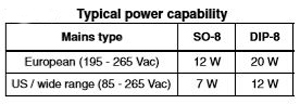
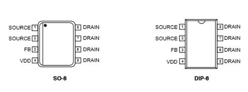
In the above image, the typical power rating of VIPer22A IC is shown. However, there is no specified section for open frame or adapter type power output specification. We will make the SMPS in open frame and for the European input rating. In such segment VIPer22A could provide 20W output. We will use it for 12W output. The VIPer22A IC pinout is given in the below image.
Designing a VIPer22APower supply circuit
The best way to build the circuit is by using Power Supply Design software. You can download the VIPer Design Software Version 2.24 to use VIPer22A, the latest version of this software no longer supports VIPer22A. It is excellent power supply design software from STMicroelectronics. By providing the design requirement info, the complete power supply circuit diagram can be generated. The VIPer22A circuit for this project generated by the software is shown below

Before going straight into building the prototype part, let's explore the circuitry operation. The circuit has the following sections -
- Input surge and SMPS fault protection
- Input Filter
- AC-DC conversion
- Driver circuitry or Switching circuit
- Clamp circuit.
- Magnetics and galvanic isolation.
- EMI filter
- Secondary Rectifier
- Filter Section
- Feedback section.
Input surge and SMPS fault protection.
This section consists of two components, F1 and RV1. F1 is a 1A 250VAC slow blow fuse and RV1 is a 7mm 275V MOV (Metal Oxide Varistor). During a high voltage surge (more than 275VAC), the MOV became dead short and blows the input Fuse. However, due to the slow blow feature, the fuse withstands inrush current through the SMPS.
Input Filter
The capacitor C3 is a 250VAC line filter capacitor. It is an X type capacitor similar to the one that we used in our transformer less power supply circuit design.
AC-DC conversion.
The AC DC conversion is done using DB107 full bridge rectifier diode. It is a 1000V 1A rated rectifier diode. The filtering is done using the 22uF 400V capacitor. However, during this prototype, we used a very large value of capacitor. Instead 22uF, we used 82uF capacitor due to the availability of the capacitor. Such high value capacitor is not required for the operation of the circuit. 22uF 400V is sufficient for 12W output rating.
Driver circuitry or switching circuit.
VIPer22A requires power from the bias winding of the transformer. After getting the bias voltage, VIPer starts switching across the transformer using an in-built high voltage mosfet. D3 is used for converting the AC bias output to a DC and the R1, 10 Ohm resistor is used for controlling the inrush current. The filter capacitor is a 4.7uF 50V for smoothening out the DC ripple.
Clamp circuit
The transformer acts a huge inductor across the power driver IC VIPer22. Therefore, during the switching off-cycle, the transformer creates high voltage spikes due to the leakage inductance of the transformer. These high-frequency voltage spikes are harmful to the power driver IC and can cause failure of the switching circuit. Thus, this needs to be suppressed by the diode clamp across the transformer. D1 and D2 are used for the clamp circuit. D1 is the TVS diode and D2 is an ultra-fast recovery diode. D1 is used for clamping the voltage whereas D2 is used as a blocking diode. As per the design, the targeted clamping voltage (VCLAMP) is 200V. Therefore, P6KE200A is selected and for ultra-fast blocking related issues, UF4007 is selected as D2.
Magnetics and galvanic isolation.
The transformer is a ferromagnetic transformer and it not only converts the high voltage AC to a low voltage ac but also provide galvanic isolation. It has three winding orders. Primary, Auxiliary or Bias winding and the Secondary winding.
EMI filter.
EMI filtering is done by the C4 capacitor. It increases the immunity of the circuit to reduce the high EMI interference. It is a Y-Class capacitor with a voltage rating of 2kV.
Secondary Rectifier and snubber circuit.
The output from the transformer is rectified and converted to DC using D6, a Schottky rectifier diode. As the output current is 2A, 3A 60V diode is selected for this purpose. SB360 is 3A 60V rated Schottky diode.
Filter Section.
C6 is the filter capacitor. It is a Low ESR capacitor for better ripple rejection. Also, an LC post-filter is used where L2 and C7 provide better ripple rejection across the output.
Feedback section.
The output voltage is sensed by the U3 TL431 and R6 and R7. After sensing the line, U2, the Optocoupler is controlled and galvanically isolating the secondary feedback sensing portion with the primary side controller. The PC817 is an Optocoupler. It has two sides, a transistor and an LED inside of it. By controlling the LED, the transistor is controlled. Since the communication is done by optically, it has no direct electrical connection, therefore satisfying the galvanic isolation on the feedback circuit too.
Now, as the LED directly controls the transistor, by providing sufficient bias across the Optocoupler LED, one can control the Optocoupler transistor, more specifically driver circuit. This control system is employed by the TL431. A shunt regulator. As the shunt regulator has a resistor divider across it reference pin, it can control the Optocoupler led which is connected across it. The feedback pin has a reference voltage of 2.5V. Therefore, the TL431 can be active only if the voltage across the divider is sufficient. In our case, the voltage divider is set to a value of 5V. Therefore, when the output reaches 5V the TL431 gets 2.5V across the reference pin and thus activate the Optocoupler's LED which controls the transistor of the Optocoupler and indirectly controls the TNY268PN. If the voltage is not sufficient across the output the switching cycle is immediately suspended.
First, the TNY268PN activates the first cycle of switching and then sense its EN pin. If everything is alright, it will continue the switching, if not, it will try once again after sometime. This loop gets continued until everything gets normal, thus preventing short circuit or overvoltage issues. This is why it is called flyback topology, as the output voltage is flown back to the driver for sensing related operations. Also, the trying loop is called a hiccup mode of operation on the failure condition.

Construction of Switching Transformer for VIPER22ASMPS Circuit
Let's see the generated transformer construction diagram. This diagram is obtained from the power supply design software that we discussed earlier.
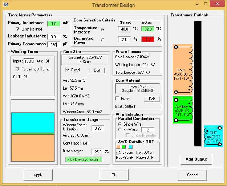
The Core is E25/13/7 with an air gap of 0.36mm. The primary inductance is 1mH. For the construction of this transformer, the following things are needed. If you are new to transformer construction please read the article on how to build your own SMPS transformer.
- Polyester Tape
- E25/13/7 Core pairs with 0.36mm air gap.
- 30 AWG copper wire
- 43 AWG copper wire (We used 36 AWG due unavailability)
- 23 AWG (We used 36 AWG too for this one)
- Horizontal or Vertical Bobbin (We used Horizontal Bobbin)
- A Pen for holding the Bobbin during winding.
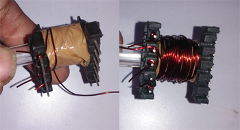
Step 1: Hold the Core using a pen, start 30 AWG copper wire from pin 3 of the bobbin and continue 133 turns clockwise to the pin 1. Apply 3 layers of polyester tape.
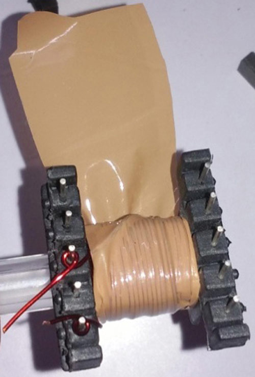
Step 2: Start the Bias winding using 43 AWG copper wire from pin 4 and continue to the 31 turns and end the winding at pin 5. Apply 3 layers of polyester tape.
Start the Bias winding using 43 AWG copper wire from pin 4 and continue to the 31 turns and end the winding at pin 5. Apply 3 layers of polyester tape.
Step 3: Start the secondary winding from pin 10 and continue clockwise winding of 21 Turns. Apply 4 layers of polyester tape.
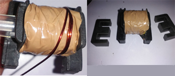
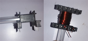
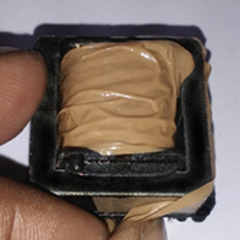
Step 4: Secure the gapped core with the duct tape wrapping side by side. This will reduce the vibration during high-density flux transfer.
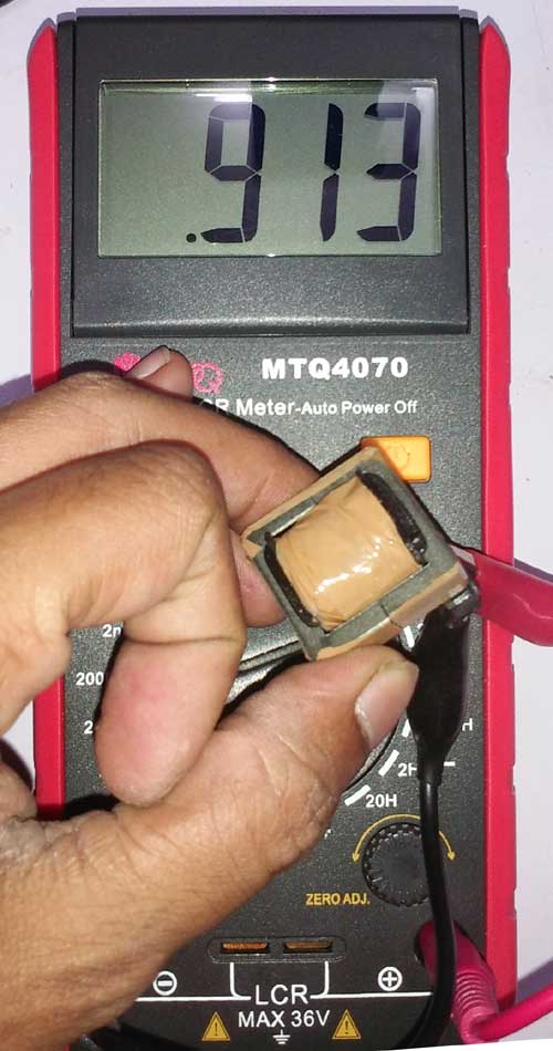
Once the build is done the transformer is tested with an LCR meter to measure the inductance value of the coils. The meter is showing 913 mH which is close to the 1mH primary inductance.
Building the VIPer22A SMPS circuit:
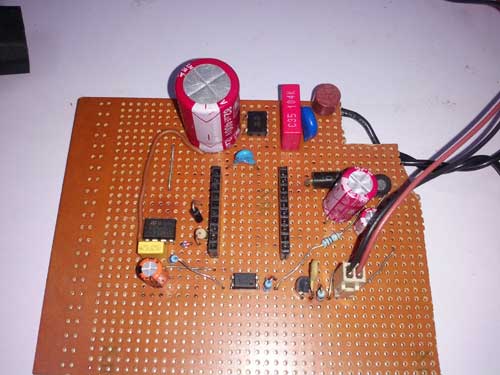
With the rating of transformer verified we can proceed with soldering all the components on a Vero board as given in the circuit diagram. My board once the soldering job was done looked like this below

Testing VIPer22A circuit for 12V 1A SMPS:
To test the circuit I connected the input side to the mains power supply through a VARIAC to control the input AC mains voltage. In the below image, the output voltage at 225VAC is shown.
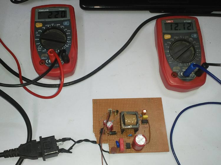
As you can see on the output side we get 12.12V which is close to the desired 12V output voltage. The complete working is shown in the video attached at the bottom of this page. Hope you understood the tutorial and learnt how to build your own SMPS circuits with a handmade transformer. If you have any questions leave them in the comment section below.
Comments
The copper wire you are using is enamelled copper wire or plain non insulated copper wire.
Hai,
Can I design this power supply with9v2a output but with inductor instead of transformer....how can I choose this inductance value for this output requirements.for wide range input85-265vac

TThankk You for this Tutorial. But Components shwon in Viper Software shown are not easily available in Indian Local Shops. Can you Share your your BOM and How much it cost you in India INR? Please also share Simmilar Component list if you have any.