
As many of us know, an Integrated Circuit or IC is a combination of many small circuits in a small package which together perform a common task. An Operational Amplifier or 555 Timer IC is built by a combination of many Transistors, Flip-Flops, Logic Gates and other combinational digital circuits. Similarly, a Flip-Flop can be built by using a combination of Logic Gates and the Logic Gates themselves can be built by using a few Transistors.
Logic Gates are the basics of many digital electronic circuits. From the basic Flip-Flops to Microcontrollers, Logic gates form the underlying principle of how bits are stored and processed. They state the relation between every input and output of a system using an arithmetic logic. There are many different types of logic gates and each of them has a different logic which be used for different purposes. But the focus of this article will be on the AND Gate because later we will be building an AND Gate using a BJT transistor circuit. Exciting right? Let's get started.
Table of Contents
What is an AND Logic Gate?
The AND logic gate is a D-shaped logic gate with two inputs and one output, where the D shape in between the inputs and outputs is the logic circuit. A BJT (Bipolar Junction Transistor) AND gate using transistor is a basic logic gate in digital electronics, and there is nothing complicated about making an AND gate with a BJT. This gate produces a HIGH output only when both of the inputs are HIGH, making it an important part of any digital circuit design. The relation between input and output values can be explained using the AND Gate Truth Table shown below.
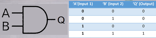
The equations output can be easily explained using the AND Gate Boolean Equation, which is Q = A x B or Q = AB. Hence, for an AND Gate, the output is HIGH only when both the inputs are HIGH.
Transistor
A transistor is a semiconductor device with three terminals that can be connected to an external circuit. The device can be used as a switch and also as an amplifier to change the values or control the passing of an electrical signal.
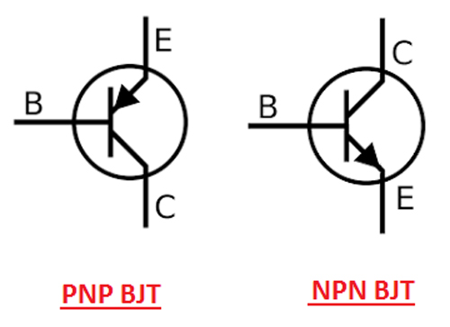
For building an AND logic gate using a transistor, we would be using BJT transistors, which can be further classified into two types: PNP and NPN – Bipolar Junction Transistors. The circuit symbol for each of them can be seen below.
This article will explain to you how to build an AND Gate circuit using a transistor. The logic of an AND gate is explained above already, and to build an AND gate using a transistor, we will follow the same truth table shown above.
Components Required for an AND Gate Using Transistor
The list of components required to build an AND gate using an NPN transistor is listed as follows:
- Two NPN transistors. (You can also use a PNP transistor if available)
- Two 10KΩ resistors & one 4-5KΩ resistor.
- One LED (Light Emitting Diode) to check the output.
- A Breadboard.
- A +5V Power supply.
- Two PUSH buttons.
- Connecting Wires.
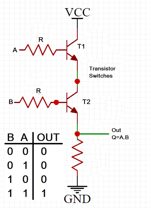
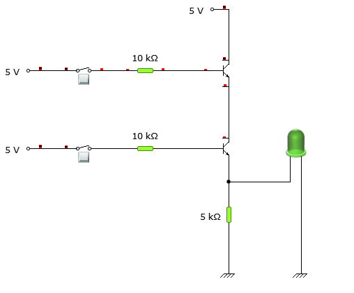
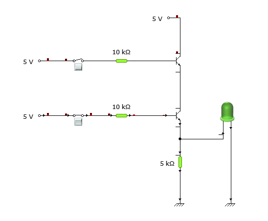
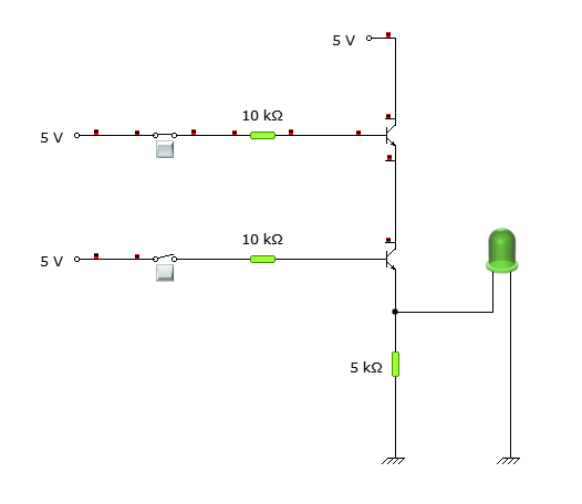
AND Gate Circuit Diagram Using Transistor
The circuit represents both the inputs A & B for the AND gate and Output, Q, which also has a +5V supply to the collector of the first transistor, which is connected in series to the second transistor, and an LED is connected to the emitter terminal of the second transistor. The inputs A & B are connected to the base terminal of Transistor 1 and Transistor 2, respectively, and the output Q goes to the positive terminal LED. The diagram below represents the above-explained circuit to build an AND gate using an NPN Transistor.
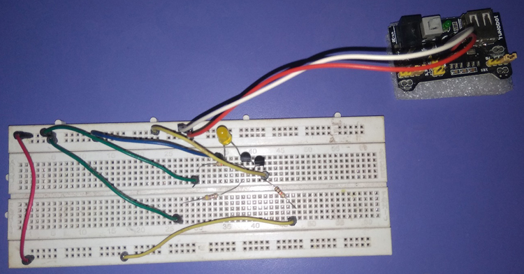
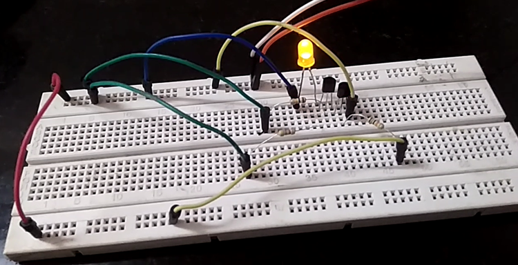
The Transistors used in this tutorial are BC547 NPN transistors and were added with all the above-mentioned components in the circuit, as shown below.
AND Gate Using Transistor on Breadboard - Assembly Guide

If you do not have the push buttons with you, you can also use wires as a switch by adding or removing them whenever required (instead of pressing the switch). The same could be seen in the video where I would use the wires as a switch connected to the base terminal for both the transistors.
The same circuit, when built using the above-mentioned hardware components, the circuit would look something like the image below.
Working Principle of the AND Gate Using Transistor
Here we will be using the transistor as a switch, and so, when a voltage is applied through the Collector terminal of the NPN transistor, the voltage reaches the Emitter Junction only when the Base Junction has a voltage supply between 0V and Collector Voltage.
Similarly, the circuit above would make the LED glow, i.e. the output is 1 (High) only when both the inputs are 1 (High), i.e. when there is a voltage supply at the base terminal of both the transistors. Meaning, there will be a straight line current path from VCC (+5V power supply) to the LED and further to the ground. In all the cases, the output will be 0 (Low) and the LED will be OFF. These all can be explained in more detail by understanding each case one by one.
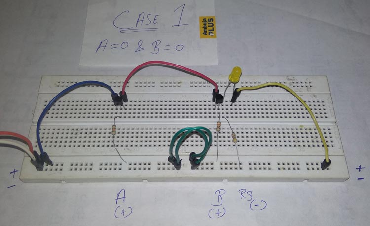
Case 1: When both inputs are zero – A = 0 & B = 0.
When both the inputs A & B are 0, you need not press any of the pushbuttons in this case. If you are not using the push buttons, then remove the wires connected to the push buttons and the base terminal of both transistors. So, we got both inputs A & B as 0, and now we need to check for the output, which also should be 0 according to the AND gate truth table.
Now, when a voltage is supplied through the collector terminal of Transistor 1, the emitter doesn’t receive any input because the base terminal value is 0. Similarly, the emitter of transistor 1, which is connected to the collector of Transistor 2, supplies no current or voltage and also the base terminal value of transistor 2 is 0. So, the 2nd transistor’s emitter outputs the value 0, and as a result, the LED would be OFF.
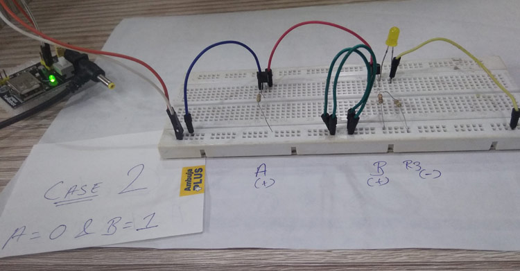
Case 2: When the inputs are – A = 0 & B = 1.
In the second case, when the inputs are A = 0 & B = 1, the circuit has the first input as 0 (Low) and the second input as 1 (High) to the base of transistors 1 & 2, respectively. Now, when a 5V supply is passed to the collector of the first transistor, then there is no change in the phase shift of the transistor since the base terminal has 0 input. Which passes 0 value to the emitter and the emitter of the first transistor is connected to the collector of the second transistor in series, so 0 value goes into the collector of the second transistor.
Now, the second transistor has a high value in the base, so it would allow the same value received in the collector to pass to the emitter. But since the value is 0 in the collector terminal of the second transistor, that’s why the emitter will also be 0, and the LED connected to the emitter would not glow.
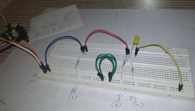
Case 3: When the inputs are – A = 1 & B = 0.
Here, the input is 1 (high) for the first transistor base and low for the second transistor base. So, the current path will start from a 5V power supply to the collector of the second transistor, passing through the collector and emitter of the first transistor, since the base terminal value is high for the first transistor.
But in the second transistor, the base terminal value is 0, and so, no current passes from the collector to the emitter of the second transistor and as a result, the LED would still be OFF only.
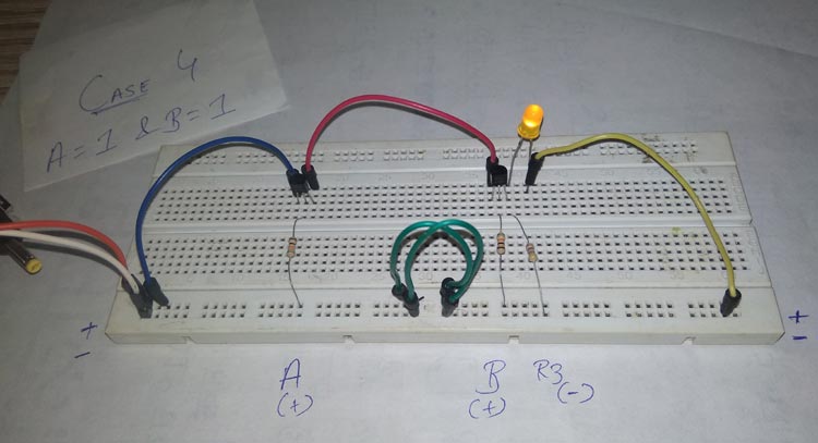
Case 4: When both inputs are one – A = 1 & B = 1.
In the last case and here both inputs are supposed to be high, which are connected to the base terminals of both the transistors. This means whenever a current or voltage passes through the collector of both the transistors, the base reaches its saturation and the transistor conducts.
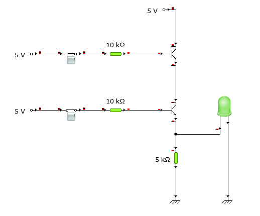
Practically speaking, when a +5V supply is provided to the collector terminal of transistor 1 and also the base terminal is saturated, then the emitter terminal would receive a high output since the transistor is forward biased. This high output at the emitter goes directly to the collector of 2nd transistor through a series connection. Now, similarly, at the second transistor, the input at the collector is high, and in this case, the base terminal is also high, meaning the second transistor is also in a saturated state, and the high input would pass from the collector to the emitter. This high output at the emitter goes to the LED, which turns the LED ON.
Troubleshooting Common Issues
| Problem | Possible Cause | Solution |
| LED always OFF | Power supply issue | Check +5V connection |
| LED always ON | Short circuit | Verify transistor connections |
| Incorrect logic | Wrong wiring | Double-check circuit diagram |
| Dim LED | High resistance | Check resistor values |
Hence, all four cases have the same inputs and outputs as the actual AND logic gate. Thus, we have built an AND Logic gate using a Transistor. Hope you understood the tutorial and enjoyed learning something new. The complete working of the setup can be found in the video below. In our next tutorial, we will also learn how to build an OR gate using a transistor and a NOT gate using a Transistor. If you have any questions, leave them in the comment section below or use our forums for other technical questions.
FAQ - AND Gate Using Transistor
⇥ What type of transistors are most appropriate for making AND gates?
BC547, BC548, or 2N2222 NPN transistors are appropriate for making AND gates. They are general-purpose transistors which provide good switching characteristics, a good current gain, and are readily available for prototyping / educational circuits.
⇥ How to make an AND gate with a transistor on a breadboard?
Connect two NPN transistors in series. Connect the collector of Q1 to +5V. Connect the Q1 emitter to the collector of Q2. Connect the emitter of Q2 to ground through an LED. Familiarise yourself with how the transistor is connected on the breadboard before working through this exercise. Insert 10kΩ base resistors for inputs A and B so these resistors connect to the appropriate transistor bases.
⇥ What is the Boolean equation for an AND gate?
The Boolean equation for an AND gate is Q = A × B or Q = A..B. The output Q is TRUE only if both inputs A AND B are TRUE at the same time.
⇥ Why do the resistors need to be used in the transistor AND gate?
Resistors limit the base current to safe values to prevent damaging the transistors, provide a level of biasing for both to enable switching action and limit the current to the LED. Base resistors allow for a clean switching effect, clearly identifying that the task is ON or OFF, while at the same time protecting components from being overloaded.
⇥ What voltage levels constitute HIGH and LOW in the transistor AND gate?
HIGH level will usually be +5V (logic 1) and LOW level will be 0V (logic 0). The HIGH output will be close to 4.3V owing to transistor voltage drops, whereas the LOW output will be close to 0V.
⇥ Can PNP transistors perform the same function as an AND gate?
Yes, PNP transistors could functionally implement AND gates using complementary logic systems with inverted power. Even though NPNs are more versatile because of their easy design, positive logic and better switching characteristics.
⇥ How do you test an AND gate in a transistor circuit?
Using all four possible combinations of the input pairs (00, 01, 10, and 11), switch or wire, take a reading of the output voltage or look at the LED. Only input pair 11 should output HIGH (~4.3V), and the LED will be lit!
Electronics Projects Built on Transistors
Discover how we’ve utilised transistors in different circuits and applications. From basics to practical applications, our transistor projects cover it all. The related project links are provided below.

How to Build a NAND Gate with Transistors?
In this article, we will go over how to build a NAND gate circuit with transistors. Transistors serve as the building blocks of logic gates, such as AND gates, NAND gates, OR gates, XOR gates, and other gates that are integral to integrated circuits.

How to Build an XOR Gate with Transistors?
In this article, we will explore the inner workings of the XOR gate, including its truth table, logical symbol representation, circuit diagram, and practical construction using transistors.

In this tutorial, we will talk about the NPN transistors. Let us consider the two examples of NPN transistors - BC547A and PN2222A, shown in the images above.

Help!
My son and I built this gate using the exact same materials (and in fact have built this same AND gate using other tutorials as well. EVERY time case 2 doesn't work: one button is pressed, the other is not and the light STILL turns on.
Does anyone have any insight as to why that might be happening?
Thank you for your help!
Brooke