

Tone control or Active equalizer circuit especially bass, treble, and MID control based Equalizer is an important circuit in audio amplifier design. Generally, three-stage active Equalizer filters require three control bass, treble, and MID. The bass control allows the low frequency to pass but blocks high frequency and the treble control allows the high frequency to pass but blocks low frequency, whereas the MID control balances between high and low frequency. In this project, we will design an active Tone control circuit powered by an op-amp with a PCB design. It will work with a 12V power supply and will have bass, treble, and mid-frequency control so that the output audio can be adjusted as required. You can also check out the other bass treble circuits which we have build earlier.
- Stereo Audio Pre-Amplifier with Bass and Treble control using Transistors
- Simple Audio Tone Control Circuit with Bass and Treble Control
- High Power Bass and Treble Control Circuit using LA4440
For this project we used PCBWay's PCB manufacturing services to make our circuit boards. In the following sections of the article we have covered the complete procedure to design, order and assemble the PCB boards for this audio equalizer circuit.
Components Required
The components required to build this Tone control circuit using Op-Amp is given below.
- 100k- potentiometer - 2 pcs
- 470k- potentiometer - 1 pcs
- TL072 operational amplifier
- 12V power supply
- .1uF 35V Capacitor
- 1.2nF 63V Capacitor
- 100uF, 35V
- 10uF, 35V
- 2.2uF, 63V
- 22k resistor
- 22nF 63V capacitor
- 270R resistor
- 33pF capacitor
- 4.7nF 63V capacitor - 2 pcs
- 47nF
- 1.8k - 2 pcs
- 10uF, 25V - 2 pcs
- 3.3k - 2pcs
- 47k - 2pcs
- 10k - 5pcs
- PCB
Audio Equalizer Circuit Diagram
The complete bass treble circuit diagram is shown in the image below. The major component in this circuit is the Op-Amp. The Op-Amp TL072 is a popular operational amplifier that has two individual operational amplifiers in a single monolithic package.

The explanation of the circuit is as follows, but you can also skip to the video at the end of this page which also explains how the circuit works. The below image shows the pinout of TL072P Op-Amp. These two operational amplifiers are depicted in the schematic as IC1A and IC1B.
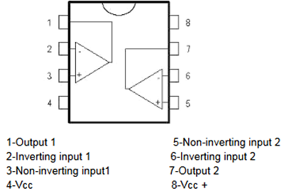
Op-Amp Buffer Circuit:
The IC1A is configured as an inverting buffer amplifier. This buffer amplifier provides a buffered output of the input signal to be filtered or equalized by the three-band filters. The capacitor C4 is a blocking capacitor that blocks the DC signal and only allows the AC signal to pass.

The resistors R3 and R4 need to be accurate and matched. It is recommended not to alter these two values at this stage. The output 2.2uF, C6 capacitor will pass the signal from the buffered output.
Mid Frequency, Bass and Treble Control Circuit:
In the next stage, IC1B is the actual active filter that has three pass filters connected across the negative feedback loop. Here is the actual tone filtration is happening-

The negative input is received from the 2.2uF capacitor. The op-amp IC1B is again configured as an inverting amplifier and it is taking an inverting input from the IC1A and at the output, it is again inverted.
The three-band filters are both RC filters. Since the capacitor values cannot be changed, the resistor value is changed over here by using a variable potentiometer. Here, the resistor R12 and capacitor C11 are used as the gain setting. Changing the R12 value will also change the gain.
In the first filter that is the bass filter (low pass). The first network circuit is R8, Bass potentiometer and R9 is the total resistance of the filter and the capacitor is C7. To determine the cutoff frequency, one can use the below formula-
fc = 1 / 2piCR
The fc is the cut off frequency and C is the capacitor value, the R is the total resistance of the network. Therefore, changing in different pot values or changing the C7 capacitor will change the frequency response of the Bass filter (Low Pass filter).
Calculating Cutoff Frequency for Bass and Treble Circuit:
For example, in the above circuit, the potentiometer value is 100k. Therefore, The total resistance, 100k (Bass Pot) + 10k (R8) + 10k (R9) = 120k. Thus as per the formula, the bass control could process the frequency up to 28 Hz.
The same thing happens for the MID filter. But instead of a low pass or high pass filters, it uses a bandpass filter construction.
The cutoff frequency can be obtained using the same formula fc = 1 / 2piCR. The highest band can be calculated using the resistor R6 and capacitor C8 (as per the schematic value, it is 10.2 kHz) and the lowest band can be calculated using the - MID potentiometer value + R10 as the total resistance and capacitor C9 (as per the schematic value, it is 70 Hz).
In the last filter band, it is a treble tone control with a high pass filter. The formula doesn't change, it is the same fc = 1 / 2piCR. The total resistor is the Treble resistor, and the R11 and the capacitor are the C10. When the treble is completely low, that means the potentiometer is fully 470k using the schematic value, the cutoff frequency of the filter is - 71 Hz. But during the full treble mode, when the potentiometer is completely turned on, the resistance of the potentiometer becomes insignificant and only the resistor R11 takes into effect. In this situation, the cutoff frequency became -18 kHz. The output is obtained from the C12.
Biasing/Offset Circuit:
Since this is a single rail supply voltage where the negative rail is not used, the input signal needs to be offset. This is due to the inability of the op-amp to amplify negative peaks of the input signal in a single rail power supply mode.
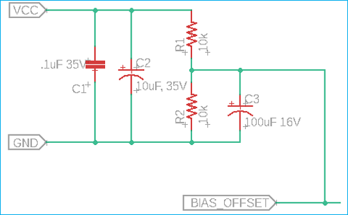
To make the offset, a voltage divider is placed across the positive feedback of the op-amp. The voltage divider will offset the signal half of the supply voltage. Since it is using 12V supply, the input signal is offset by 6V DC. The C1 and C2 are the filter capacitors and the R1 and R2 are used to make the voltage divider along with an additional filter capacitor C3.
Active Audio Filter PCB Design
The PCB for our Active Audio Filter circuit is designed for a double sideboard. I have used Eagle to design my PCB but you can use any Design software of your choice. The 2D image of my board design is shown below.
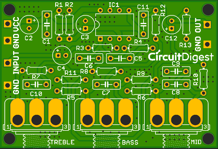
Sufficient ground filling vias are used to properly create the ground path all over the circuit board. The input signal and the input voltage section are created on the left-hand side and the output is created on the right-hand side for better usability. The complete Design file for Eagle along with the Gerber can be downloaded from the link below.
Now, that our Design is ready, it is time to get them fabricated using the Gerber file. To get the PCB done is quite easy, simply follow the steps below-
Ordering PCB from PCBWay
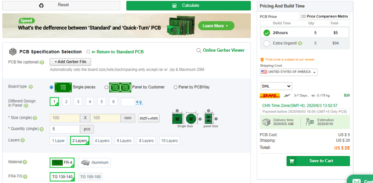
Step 1: Get into https://www.pcbway.com/, sign up if this is your first time. Then, in the PCB Prototype tab, enter the dimensions of your PCB, the number of layers, and the number of PCB you require.
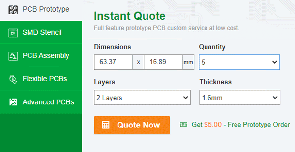
Step 2: Proceed by clicking on the ‘Quote Now’ button. You will be taken to a page where to set a few additional parameters if required, like the material used, track spacing, etc. But mostly, the default values will work fine.
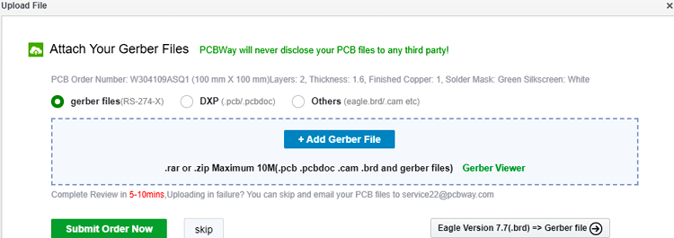
Step 3: The final step is to upload the Gerber file and proceed with the payment. To make sure the process is smooth, PCBWAY verifies if your Gerber file is valid before proceeding with the payment. This way, you can sure that your PCB is fabrication friendly and will reach you as committed.
Assembling and Testing the Active Audio Filter Circuit
After a few days, we received our PCB in a neat package. The PCB quality and packaging was good as always. You can see the packaging for yourself.
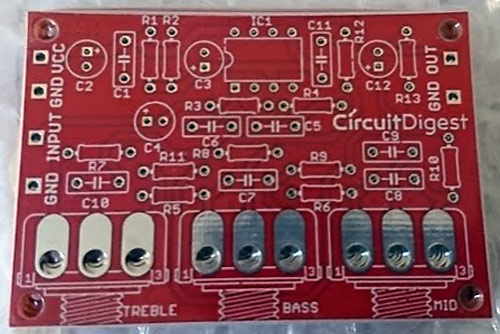
The top layer and the bottom layer of the board are shown in the below image. We have chosen red as the solder mask, simply because it is attractive and PCBway provides all mask colors for the same price, so why not have fun with PCB colour.
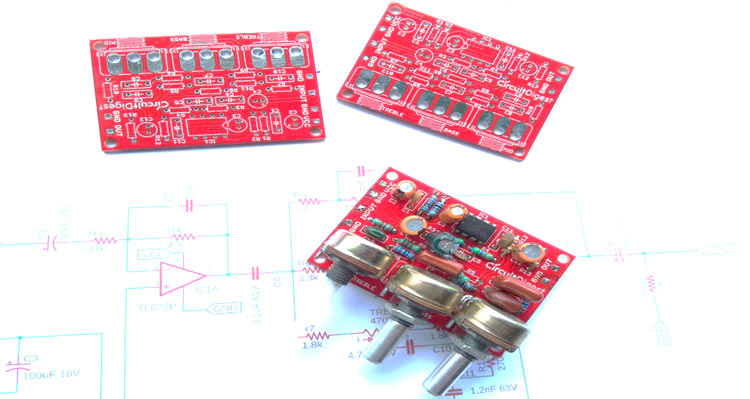
As you can notice from the above image, the quality of the PCB is very good. The tracks, the pads, vias, and other clearances were all perfectly fabricated. I began assembly my board as soon as I received it. You can see the assembled board below.
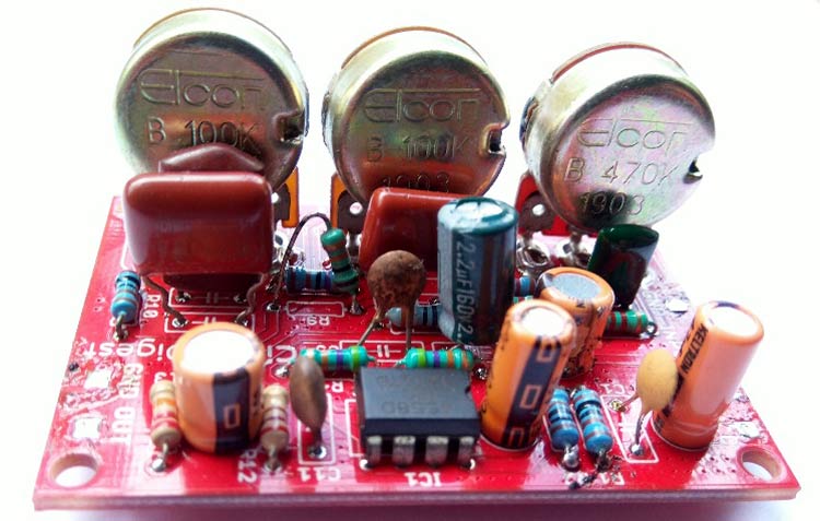
However, for a few capacitors, the voltage ratings are not accurate as required but it does not make any differences in the circuit output. Also, the operational amplifier TL072 is replaced with JRC4558 due to the unavailability of the IC. Other Op-Amp IC can also work but the pin mapping must be matched with the standard op-amp pin mapping.
The circuit is tested using an audio input from a laptop, a 12V power supply, and a 15W 2.1 Speaker output system. The detailed working and testing information can be found in the video below.
Hope you enjoyed the tutorial and learned something useful. If you have any questions or doubts, leave them in the comment section below. You can also use our forums for other technical questions.
Comments
like this pic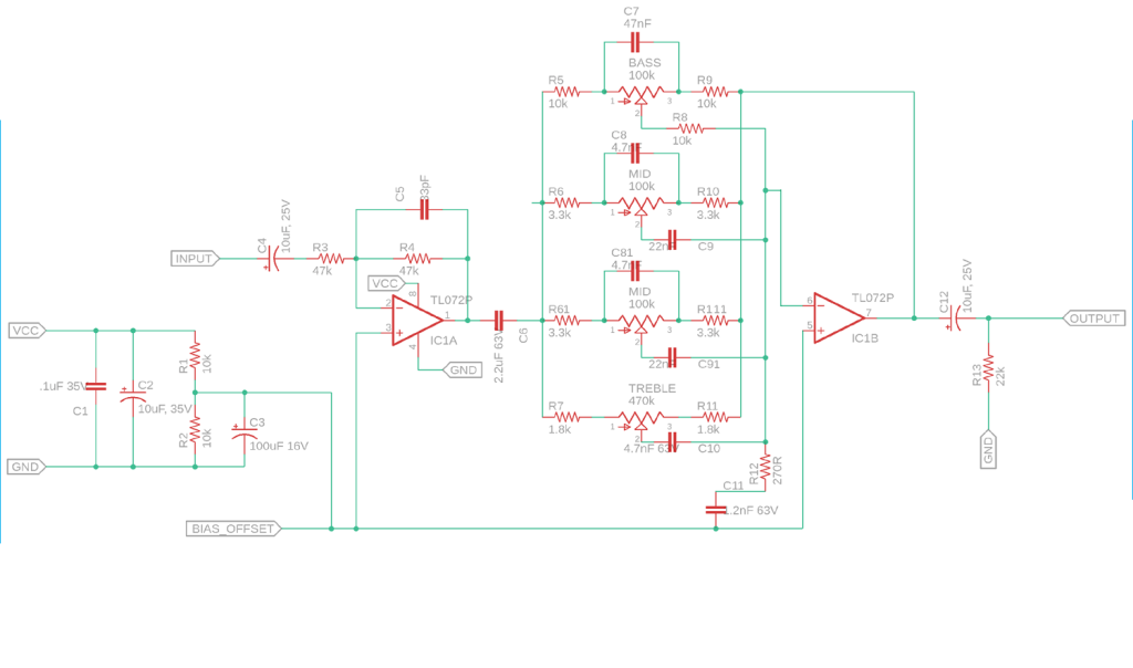
I need to populate the component under bread board

Hi, thanks for good post
can I add another mid control to it and have low mid and high mid control ?