
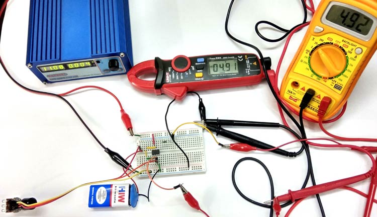
Voltage Follower is simply a circuit in which output follows the input, means output voltage remains same as input voltage. It is also commonly known as Unity gain Opamp Amplifier or Opamp Buffer. Here we construct a voltage follower using Opamp LM741 and see how its output follows the input. We already discussed about it in our Non-inverting Operational Amplifier tutorial, here we will build it with real hardware and test it.
Components Required
- Opamp LM741 - 1 nos
- Potentiometer - 1 nos
- Resistor 1k - 1nos
- Input 9V DC
- Opamp Supply 12V DC
- Multimeter - 2 nos
- Connecting wires
OP-amp IC LM741
LM741 operational amplifier is a DC-coupled high gain electronic voltage amplifier. It’s a small chip having 8 pins. An operational amplifier IC is used as a comparator which compares the two signal, the inverting and non-inverting signal. In Op-amp IC 741 PIN2 is an inverting input terminal and PIN3 is non-inverting input terminal. The output pin of this IC is PIN6. The main function of this IC is to do the mathematical operation in various circuits.
When the voltage at non-inverting input (+) is higher than the voltage at inverting input (-), then the output of the comparator is High. And if the voltage of inverting input (-) is Higher than the non-inverting end (+), then the output is LOW. In this Wireless Switch Circuit, LM741 is used to provide the Low to high Clock pulse to IC 4017, for each time when one passes a hand over the LDR. Learn more about Op-amp 741 here.
Pin diagram of LM741
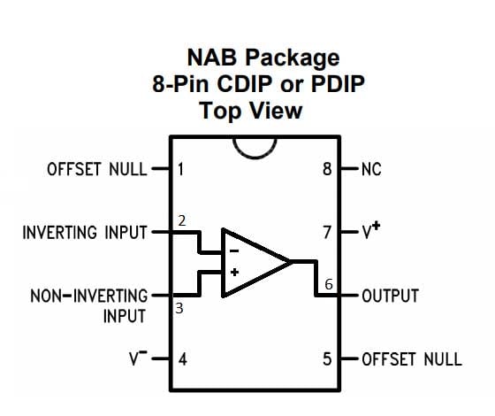
Pin Configuration of LM741
|
PIN NO. |
PIN Description |
|
1 |
Offset null |
|
2 |
Inverting (-) input terminal |
|
3 |
non-inverting (+) input terminal |
|
4 |
negative voltage supply (-VCC) |
|
5 |
offset null |
|
6 |
Output voltage pin |
|
7 |
positive voltage supply (+VCC) |
|
8 |
not connected |
Voltage Follower Circuit and its Working
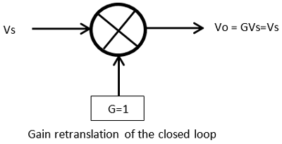
As we said that it’s a Unity gain Amplifier means the gain of the Amplifier will be 1 and whatever is fed as input, can be received as output. Below is the circuit diagram of Voltage Follower Circuit:

In above Voltage Follower Circuit, variable input is given to the non-inverting terminal of opamp and the inverting terminal is given the negative feedback from the output. By adjusting the potentiometer at the input, Vs can be varied to different value in the range of 0-9Vdc.
Gain (Av) = Vout / Vin
So, 1 = Vout / Vin
Vin = Vout.
We can say that output follows the magnitude of the input. As there is no external components in the feedback circuit and the gain is Unity (1), this voltage follower is also known as Unity Gain Buffer.
The input impedance of the op-amp is very high when a voltage follower or unity gain configuration is used. Sometimes the input impedance is much higher than 1 Megohm. So, due to high input impedance, we can apply weak signals across the input and no current will flow in the input pin from the signal source to amplifier. On the other hand, the output impedance is very low, and it will produce the same signal input, in the output.
Voltage follower circuit is used to create isolation between two different kind of circuits. Due to high input impedance,, so the input current is much lower than the output current while the output voltage follows the input voltage. So the voltage follower provides large power gain across its output. Due to this behavior, Voltage follower used as a buffer circuit and can be used to isolate stages while building multistage filters or some other multistage circuit.
