

Op-Amp, short for operational amplifier is the backbone of Analog electronics. An operational amplifier is a DC-coupled electronic component which amplifies Voltage from a differential input using resistor feedback. Op-Amps are popular for its versatility as they can be configured in many ways and can be used in different aspects. An op-amp circuit consists of few variables like bandwidth, input, and output impedance, gain margin etc. Different class of op-amps has different specifications depending on those variables. There are plenty of op-amps available in different integrated circuit (IC) package, some op-amp ic’s has two or more op-amps in a single package. LM358, LM741, LM386 are some commonly used Op-amp ICs. You can learn more about Op-amps by following our Op-amp circuits section.
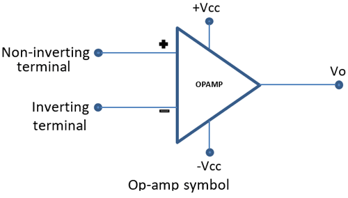
An op-amp has two differential input pins and an output pin along with power pins. Those two differential input pins are inverting pin or Negative and Non-inverting pin or Positive. An op-amp amplifies the difference in voltage between this two input pins and provides the amplified output across its Vout or output pin.
Depending on the input type, op-amp can be classified as Inverting or Non-inverting. In this tutorial, we will learn how to use op-amp in noninverting configuration.
In the non-inverting configuration, the input signal is applied across the non-inverting input terminal (Positive terminal) of the op-amp. Due to this, the amplified output become “in- phase” with the input signal.
As we discussed before, Op-amp needs feedback to amplify the input signal. This is generally achieved by applying a small part of the output voltage back to the inverting pin (In case of non-inverting configuration) or in the non-inverting pin (In case of inverting pin), using a voltage divider network.
Non-inverting Operational Amplifier Configuration
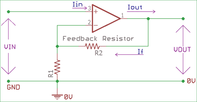
In the upper image, an op-amp with Non-inverting configuration is shown. The signal which is needed to be amplified using the op-amp is feed into the positive or Non-inverting pin of the op-amp circuit, whereas a Voltage divider using two resistors R1 and R2 provide the small part of the output to the inverting pin of the op-amp circuit. These two resistors are providing required feedback to the op-amp. In an ideal condition, the input pin of the op-amp will provide high input impedance and the output pin will be in low output impedance.

The amplification is dependent on those two feedback resistors (R1 and R2) connected as the voltage divider configuration. R2 is referred to as Rf (Feedback resistor)
The Voltage divider output which is fed into the non-inverting pin of the amplifier is equal to the Vin, as Vin and voltage divider’s junction points are situated across the same ground node.
Due to this, and as the Vout is dependent on the feedback network, we can calculate the closed loop voltage gain as below.
Gain of Non-inverting Op-amp

As Voltage Divider output Voltage is same as input Voltage, Divider Vout = Vin
So, Vin / Vout = R1 / (R1 + Rf)
Or, Vout / Vin = (R1 + Rf) / R1
The total voltage gain of the amplifier (Av) is Vout / Vin
So, Av = Vout / Vin = (R1 + Rf) / R1
Using this formula we can conclude that the closed loop voltage gain of a Non- Inverting operational amplifier is,
Av = Vout / Vin = 1 + (Rf / R1)
So, by this factor, the op-amp gain cannot be lower than unity gain or 1. Also, the gain will be positive and it cannot be in negative form. The gain is directly dependent on the ratio of Rf and R1.
Now, Interesting thing is, if we put the value of feedback resistor or Rf as 0, the gain will be 1 or unity. And if the R1 becomes 0, then the gain will be infinity. But it is only possible theoretically. In reality, it is widely dependent on the op-amp behavior and open-loop gain.
Op-amp can also be used two add voltage input voltage as summing amplifier.
Practical Example of Non-inverting Amplifier
We will design a non-inverting op-amp circuit which will produce 3x voltage gain at the output comparing the input voltage.
We will make a 2V input in the op-amp. We will configure the op-amp in noninverting configuration with 3x gain capabilities. We selected the R1 resistor value as 1.2k, We will find out the value of Rf or R2 resistor and will calculate the output voltage after amplification.
As the gain is dependent on the resistors and the formula is Av = 1 + (Rf / R1)
In our case, the gain is 3 and the value of R1 is 1.2k. So, the value of Rf is,
3 = 1 + (Rf / 1.2k)
3 = 1 + (1.2k + Rf / 1.2k)
3.6k = 1.2k + Rf
3.6k - 1.2k = Rf
Rf = 2.4k
After amplification, the output voltage will be
Av = Vout / Vin
3 = Vout / 2V
Vout = 6V

The example circuit is shown in the above image. R2 is the feedback resistor and the amplified output will be 3 times than the input.
Voltage Follower or Unity Gain Amplifier
As discussed before, if we make Rf or R2 as 0, that means there is no resistance in R2, and Resistor R1 is equal to infinity then the gain of the amplifier will be 1 or it will achieve the unity gain. As there is no resistance in R2, the output is shorted with the negative or inverted input of the op-amp. As the gain is 1 or unity, this configuration is called as unity gain amplifier configuration or voltage follower or buffer.
As we put the input signal across the positive input of the op-amp and the output signal is in phase with the input signal with a 1x gain, we get the same signal across amplifier output. Thus the output voltage is the same as the input voltage. Voltage out = Voltage in.
So, it will follow the input voltage and produce the same replica signal across its output. This is why it is called a voltage follower circuit.
The input impedance of the op-amp is very high when a voltage follower or unity gain configuration is used. Sometimes the input impedance is much higher than 1 Megohm. So, due to high input impedance, we can apply weak signals across the input and no current will flow in the input pin from the signal source to amplifier. On the other hand, the output impedance is very low, and it will produce the same signal input, in the output.

In the above image voltage follower configuration is shown. The output is directly connected across the negative terminal of the op-amp. The gain of this configuration is 1x.
As we know,
Gain (Av) = Vout / Vin
So, 1 = Vout / Vin
Vin = Vout.
Due to high input impedance, the input current is 0, so the input power is also 0 as well. The voltage follower provides large power gain across its output. Due to this behavior, Voltage follower used as a buffer circuit.
Also, buffer configuration provides good signal isolation factor. Due to this feature, voltage follower circuit is used in Sallen-key type active filters where filter stages are isolated from each other using voltage follower op-amp configuration.
There are digital buffer circuits also available, like 74LS125, 74LS244 etc.
As we can control the gain of the noninverting amplifier, we can select multiple resistors values and can produce a non-inverting amplifier with a variable gain range.
Non-inverting amplifiers are used in audio electronics sectors, as well as in scope, mixers, and various places where digital logic is needed using analog electronics.
