

If you have ever worked with Batteries, SMPS circuits or other Power supply circuits, then often it would have occurred that you have to test your power source by loading it to check how it performs under different loading conditions. A device that is commonly used to perform this type of test is called a Constant Current DC Load, which allows us to adjust the output current of your power source and then keeps it constant until it is adjusted again changes. In this tutorial, we will learn how to build our very own Adjustable Electronic Load using Arduino, which can take a maximum input voltage of 24V and drain current as high as 5A. For this project, we have used PCB boards which are manufactured by AllPCB, a china based professional PCB manufacturing and assembling service provider.
In our previous voltage-controlled current source tutorial, we have explained how to use an operational amplifier with a MOSFET and make use of a voltage-controlled current source circuit. But in this tutorial, we will apply that circuit and make a digitally controlled current source. Obviously, A digitally controlled current source requires a digital circuit and to serve the purpose, an Arduino NANO is used. The Arduino NANO will provide required controls for the DC load.
The circuit consists of three parts. The first part is the Arduino Nano section, the second part is the digital to analog converter, and the third part is a pure analog circuit where a dual operational amplifier in a single package is used which will control the load section. This project is inspired by a post on Arduino, however, the circuit is changed for less complexity with basic features for everyone to build it.
Our Electronic load is designed to have the following input and output sections.
- Two input switches for increasing and decreasing the load.
- An LCD that will display the set load, actual load, and the load voltage.
- The maximum load current is limited to 5A.
- The maximum input voltage is 24V for the load.
Materials Required
The components required to build a DC electronic load are listed below.
- Arduino nano
- 16x2 character LCD
- Two barrel socket
- Mosfet irf540n
- Mcp4921
- Lm358
- 5watt shunt resistor .1 ohms
- 1k
- 10k - 6pcs
- Heatsink
- .1uF 50v
- 2k - 2pcs
Arduino DC Electronic Load Circuit Diagram
In the below schematic, the operational amplifier has two sections. One is to control the MOSFET and the other one is to amplify the sensed current. You can also check the video at the bottom of this page which explains the complete working of the circuit. The first section is having R12, R13, and MOSFET. R12 is used to reduce the loading effect on the feedback section and R13 is used as the Mosfet gate resistor.

Additional two resistors R8 and R9 are used to sense the supply voltage of the power supply that will be stressed by this dummy load. As per the voltage divider rule, these two resistors support a maximum of 24V. More than 24V will produce a voltage that will be not suitable for the Arduino pins. So be careful not to connect power supply that has more than 24V output voltage.
The Resistor R7 is the actual load resistor here. It is a 5 Watt, .1 Ohm resistor. As per the power-law, it will support maximum 7A (P = I2R), but for the safe side, it is wiser to limit the load current maximum of 5A. Therefore, at present maximum 24V, 5A load can be set by this dummy load.
Another section of the amplifier is configured as a gain amplifier. It will provide 6x gain. During the flow of current, a voltage drop will appear. For example, when 5A of current is flowing through the resistor, the voltage drop will be .5V across the .1 Ohms shunt resistor (V = I x R) according to ohms law. The non-inverting amplifier will amplify it to x6, therefore 3V will be the output from the second part of the amplifier. This output will be sensed by the Arduino nano analog input pin and the current will be calculated.
The first part of the amplifier is configured as a voltage follower circuit which will control the MOSFET as per the input voltage and get the desired feedback voltage due to the load current flowing through the shunt resistor.
MCP4921 is the Digital to Analog converter. The DAC uses the SPI communication protocol to get the digital data from any microcontroller unit and provide analog voltage output depending on it. This voltage is the input of the op-amp. We have previously also learned how to use this MCP4921 DAC with PIC.
On the other side, there is an Arduino Nano which will provide the digital data to the DAC via SPI protocol and control the load, also displaying the data in the 16x2 character display. Two additional things are used, that is the decrease and increase button. Instead of connecting to a digital pin it is connected in the analog pins. Therefore, one can change it to another type of switches such as slider or analog encoder. Also, by modifying the code one can provide raw analog data to control the load. This also avoids the switch debounce problem.
Finally, by increasing the load, the Arduino nano will provide the load data to the DAC in digital format, the DAC will provide analog data to the operational amplifier, and the operational amplifier will control the MOSFET as per the input voltage of the operational amplifier. Finally, depending on the load current flow through the shunt resistor, a voltage drop will appear which will further be amplified by the second channel of LM358 and get by the Arduino nano. This will be displayed on the character display. The same thing will happen when the user presses the decrease button.
PCB Design and Gerber File
Since this circuit is having a high current path, it is a wiser choice to use proper PCB design tactics for removing unwanted failure cases. Thus, a PCB is designed for this DC load. I have used Eagle PCB Design Software to design my PCB. You can choose any PCB Cad Software. The final designed PCB in the CAD software is shown in the below image,
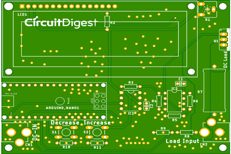
One important factor to notice during the design of this PCB is to use a thick power plane for proper current flow all over the circuit. There is also ground stitching VIAS (random vias in the ground plane) that are used for proper ground flow in both the layers to the top and bottom.
You can also download the Gerber file of this PCB from the link below and use it for fabrication.
Ordering your PCB from AllPCB
Once you are ready with your Gerber file you can use it to get your PCB fabricated. Speaking of which brings up the sponsor of this article ALLPCB, who are known for their high-quality PCBs and ultrafast shipping. Apart from PCB Manufacturing, AllPCB also provides PCB Assembly and Component Sourcing.
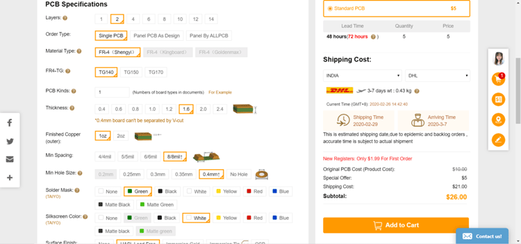
To get your PCB order from them, visit allpcb.com and signup. Then on the home page, enter the dimensions of your PCB and the required quantity as shown below. Then click on Quote now.

Now you can change the other parameters of your PCB like the number of layers, mask color, thickness, etc. On the right-hand side, you can choose your country and the preferred shipping option. This will show you the lead time and total amount to be paid. I have chosen DHL and my total amount is $26, but if you are a first time customer the prices will go down in the checkout. Then click on Add to Cart and then click on check out now.
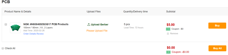
Now, you can click on upload your Gerber file by clicking on “Upload Gerber” and then click on buy.
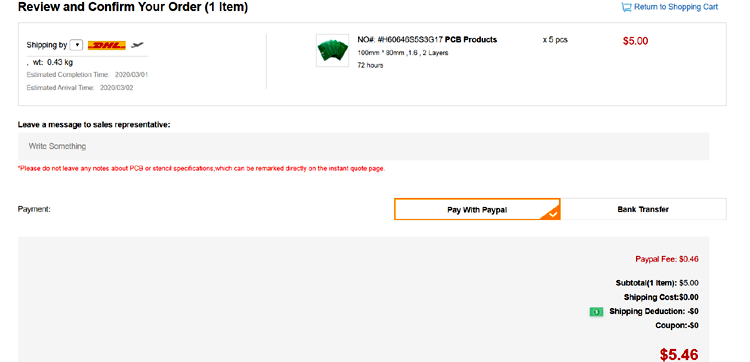
On the next page, you can enter your shipping address and check the final price you have to pay for your PCB. You can then review your order and then click on submit to make the payment.
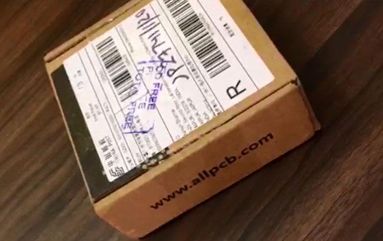
Once your order is confirmed you can sit back and relay for your PCB to arrive at your doorstep. I received my order after a few days and then packaging was neat as shown below.
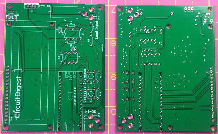
The quality of the PCB was good as always as you can see for yourself in the pictures below. The top side and the bottom side of the board are shown below.
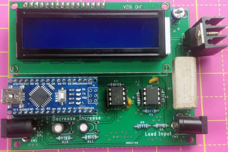
Once you get your board, you can proceed with assembling all the components. My finished board looks something like this shown below.
Next, you can upload the code and power up the module to check how it is working. The complete code for this project is given at the bottom of this page. The explanation of the code is as follows.
Arduino Code for Adjustable DC Load
The code is pretty simple. At first, we included SPI and LCD header files as well as set the maximum logic voltage, chip selection pins, etc.
#include <SPI.h>
#include <LiquidCrystal.h>
#define SS_PIN 10
#define MAX_VOLT 5.0 // maximum logic voltage
#define load_resistor 0.1 // shunt resistor value in Ohms
#define opamp_gain 6 // gain of the op-amp
#define average 10 // average time
This section consists of required program flow-related declarations of integers and variables. Also, we set the associate peripherals pins with Arduino Nano.
const int slaveSelectPin = 10; // Chip select pin
int number = 0;
int increase = A2; // Increase pin
int decrease = A3; //decrease pin
int current_sense = A0; //current sense pin
int voltage_sense = A1; // voltage sense pin
int state1 = 0;
int state2 = 0;
int Set = 0;
float volt = 0;
float load_current = 0.0;
float load_voltage = 0.0;
float current = 0.0;
float voltage = 0.0;
LiquidCrystal lcd(7, 6, 5, 4, 3, 2); // LCD pins
This is used for the Setup of LCD and SPI. Also, the pin directions are set over here.
void setup() {
  pinMode(slaveSelectPin, OUTPUT);
  pinMode(increase, INPUT);
  pinMode(decrease, INPUT);
  pinMode(current_sense, INPUT);
  pinMode(voltage_sense, INPUT);
  // initialize SPI:
  SPI.begin();
  //set up the LCD's number of columns and rows:
    lcd.begin(16, 2);
  // Print a message to the LCD.
    lcd.print("Digital Load");
    lcd.setCursor(0, 1);
    lcd.print("Circuit Digest");
    delay (2000);
}
It is used for Converting the DAC value.
void convert_DAC(unsigned int value)
{
   /*Step Size = 2^n, Therefore 12bit 2^12 = 4096
     For 5V reference, the step will be 5/4095 = 0.0012210012210012V or 1mV (approx)*/
  unsigned int container ;
  unsigned int MSB;
  unsigned int LSB;
  /*Step: 1, stored the 12 bit data into the container
   Suppose the data is 4095, in binary 1111 1111 1111*/
  container = value;
  /*Step: 2 Creating Dummy 8 bit. So, by dividing 256, upper 4 bits are captured in LSB
   LSB = 0000 1111*/
  LSB = container/256;
  /*Step: 3 Sending the configuration with punching the 4 bit data.
   LSB = 0011 0000 OR 0000 1111. Result is 0011 1111 */
  LSB = (0x30) | LSB;
  /*Step:4 Container still has the 21bit value. Extracting the lower 8 bits.
   1111 1111 AND 1111 1111 1111. Result is 1111 1111 which is MSB*/
  MSB = 0xFF & container;
 /*Step:4 Sending the 16bits data by dividing into two bytes. */
    digitalWrite(slaveSelectPin, LOW);
    delay(100);
    SPI.transfer(LSB);
    SPI.transfer(MSB);
    delay(100);
    // take the SS pin high to de-select the chip:
    digitalWrite(slaveSelectPin, HIGH);
}
This section is used for current sensing related operations.
float read_current (void){
          load_current = 0;
          for (int a = 0; a < average; a++){
          load_current = load_current + analogRead(current_sense);
        }
        load_current = load_current / average;
        load_current = (load_current* MAX_VOLT) / 1024;
        load_current = (load_current / opamp_gain) / load_resistor;
        return load_current;
}
This is used for reading the load voltage.
float read_voltage (void){
          load_voltage = 0;
          for (int a = 0; a < average; a++){
          load_voltage = load_voltage + analogRead(voltage_sense);
        }
        load_voltage = load_voltage / average;
        load_voltage = ((load_voltage * MAX_VOLT)/1024.0)*6;
        return load_voltage;
}
This is the actual loop. Here, switch steps are measured and the data is sent to the DAC. After transmitting the data, the actual current flow and the load voltage is being measured. Both values are also finally printed on the LCD.
void loop () {
        state1 = analogRead(increase);
        if (state1 > 500){
          delay(50);
           state1 = analogRead(increase);
           if (state1 > 500){
              volt = volt+0.02;
           }
        }
         state2 = analogRead(decrease);
        if (state2 > 500){
          delay(50);
           state2 = analogRead(decrease);
           if (state2 > 500){
              if (volt == 0){
                volt = 0;
              }
            else{
                volt = volt-0.02;
            }
           }
        }
        number = volt / 0.0012210012210012;
        convert_DAC (number);
        voltage = read_voltage();
        current = read_current();
         lcd.setCursor(0, 0);
         lcd.print("Set Value");
        lcd.print("=");
        Set = (volt/2)*10000;
        lcd.print(Set);
        lcd.print("mA    ");
        lcd.setCursor(0, 1);
        lcd.print("I");
        lcd.print("=");
        lcd.print(current);
        lcd.print("A ");
        lcd.print(" V");
        lcd.print("=");
        lcd.print(voltage);
        lcd.print("V");
       // lcd.print(load_voltage);
        //lcd.print("mA    ");
       // delay(1000);
        //lcd.clear();
}

Testing our Adjustable DC Load
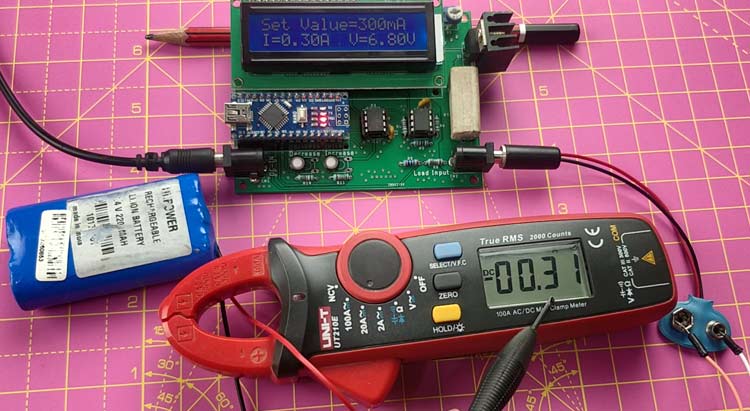
The digital load circuit is soldered and powered up using a 12V power source. I used my 7.4V Lithium battery on the power source side and connected a clamp meter to check how it is working. As you can see when the set current is 300mA the circuit draws 300mA from the battery which is also measured by clamp meter as 310mA.
The complete working of the circuit can be found in the video linked below. Hope you understood the project and enjoyed building something useful. If you have any questions leave them in the comment section or use the Forums.
Complete Project Code
#include <SPI.h>

#include <LiquidCrystal.h>

#define SS_PIN 10

#define MAX_VOLT 5.0

#define load_resistor 0.1

#define opamp_gain 6

#define average 10

const int slaveSelectPin = 10;

int number = 0;

int increase = A2;

int decrease = A3;

int current_sense = A0;

int voltage_sense = A1;

int state1 = 0;

int state2 = 0;

int Set = 0;

float volt = 0;

float load_current = 0.0;

float load_voltage = 0.0;

float current = 0.0;

float voltage = 0.0;

LiquidCrystal lcd(7, 6, 5, 4, 3, 2);

void setup() {

  // set the slaveSelectPin as an output:

  pinMode(slaveSelectPin, OUTPUT);

  pinMode(increase, INPUT);  // declare LED as output

  pinMode(decrease, INPUT);    // declare pushbutton as input

  pinMode(current_sense, INPUT);  //

  pinMode(voltage_sense, INPUT);    //

  // initialize SPI:

  SPI.begin();

  //set up the LCD's number of columns and rows:

    lcd.begin(16, 2);

  // Print a message to the LCD.

    lcd.print("Digital Load");

    lcd.setCursor(0, 1);

    lcd.print("Circuit Digest");

    delay (2000);

}

void convert_DAC(unsigned int value)

{

   /*Step Size = 2^n, Therefore 12bit 2^12 = 4096

     For 5V reference, the step will be 5/4095 = 0.0012210012210012V or 1mV (approx)*/

  unsigned int container ;

  unsigned int MSB;

  unsigned int LSB;

  /*Step: 1, stored the 12 bit data into the container

   Suppose the data is 4095, in binary 1111 1111 1111*/

  container = value;

  /*Step: 2 Creating Dummy 8 bit. So, by dividing 256, upper 4 bits are captured in LSB

   LSB = 0000 1111*/

  LSB = container/256;

  /*Step: 3 Sending the configuration with punching the 4 bit data.

   LSB = 0011 0000 OR 0000 1111. Result is 0011 1111 */

  LSB = (0x30) | LSB;

  /*Step:4 Container still has the 21bit value. Extracting the lower 8 bits.

   1111 1111 AND 1111 1111 1111. Result is 1111 1111 which is MSB*/

  MSB = 0xFF & container;

 /*Step:4 Sending the 16bits data by dividing into two bytes. */

    digitalWrite(slaveSelectPin, LOW);

    delay(100);

    SPI.transfer(LSB);

    SPI.transfer(MSB);

    delay(100);

    // take the SS pin high to de-select the chip:

    digitalWrite(slaveSelectPin, HIGH);

}

float read_current (void){

          load_current = 0;

          for (int a = 0; a < average; a++){

          load_current = load_current + analogRead(current_sense);

        }

        load_current = load_current / average;

        load_current = (load_current* MAX_VOLT) / 1024;

        load_current = (load_current / opamp_gain) / load_resistor;

        return load_current;

}

float read_voltage (void){

          load_voltage = 0;

          for (int a = 0; a < average; a++){

          load_voltage = load_voltage + analogRead(voltage_sense);

        }

        load_voltage = load_voltage / average;

        load_voltage = ((load_voltage * MAX_VOLT)/1024.0)*6;

        return load_voltage;

}

void loop () {

        state1 = analogRead(increase);

        if (state1 > 500){

          delay(50);

           state1 = analogRead(increase);

           if (state1 > 500){

              volt = volt+0.02;

           }

        }

         state2 = analogRead(decrease);

        if (state2 > 500){

          delay(50);

           state2 = analogRead(decrease);

           if (state2 > 500){

              if (volt == 0){

                volt = 0;

              }

            else{

                volt = volt-0.02;

            }

           }

        }

        number = volt / 0.0012210012210012;

        convert_DAC (number);

        voltage = read_voltage();

        current = read_current();

         lcd.setCursor(0, 0);

         lcd.print("Set Value");

        lcd.print("=");

        Set = (volt/2)*10000;

        lcd.print(Set);

        lcd.print("mA    ");

        lcd.setCursor(0, 1);

        lcd.print("I");

        lcd.print("=");

        lcd.print(current);

        lcd.print("A ");

        lcd.print(" V");

        lcd.print("=");

        lcd.print(voltage);

        lcd.print("V");

       // lcd.print(load_voltage);

        //lcd.print("mA    ");

       // delay(1000);

        //lcd.clear();

}
Comments
Hi,
Hi,
I'm looking to build this project, however, there seems to be some discrepancies between the schematic, the PCB and the build of materials (BOM) list. Can you please clarify?
The schematic shows a 560R resistor connected to pin A on the LCD, but this is not listed in the BOM.
The BOM lists a 1k resistor, but this isn't on the schematic.
2 capacitors are shown, C1 & C2, however, there are no values on the schematic and they aren't listed in the BOM.
The BOM lists a 0.1uf 50v capacitor, but this isn't on the schematic.
The 10k trimpot isn't listed in the BOM.
I hope you can help as this looks like a fun project.
Thanks
John
I have received my PCB but
I have received my PCB but there is no R12 or R13. Have you deleted them?
IC2 pin1 is directly connected to the MOSFET pin1 and
IC2 pin2 is directly connected to the MOSFET pin3 and R7

hi,
I want to make variable load of for 12.8V 30Ah battery.
please let me know what changes i have to made in the circuit.