

Switching Mode Power Supply (SMPS) is an interesting component that uses a compact design within a space of one or two inches and could be easily soldered in the PCB. It is a hot cake in this electronics industry and there are lots of companies that manufacture this thing. How nice it would be if we can build a standard SMPS circuit that could be fitted in a limited space and can be part of IoT-based applications as well as different microcontroller projects.
In this project, we will build a compact power supply with 3.3V, 1.5A power rating which serves the purposes. To build this SMPS circuit on PCB, we got fabricated our PCB boards from PCBWay and we have assembled and tested the same in this tutorial session. Please remember this is not a commercially used one and this does not have proper protections in the input. Also, since we need to make it for day-to-day hobby projects, the size of the SMPS too is crucial. It does not include any surge and fuse protection which is a must-have thing in industrial SMPS. If you want to add this, use the protections separately. Previously, we have also built a 12V 15W SMPS circuit using a PCB, so people who are interested in how to design a PCB for a PSU project (power supply unit) can check that as well.
3.3V 1.5A SMPS Circuit – Design Specifications
The SMPS will have the following specifications.
- 185VAC-230VAC input
- 3.3V up to 1.5A output.
- Open frame construction
- Short circuit protection
- Small size with low-cost features
This SMPS is designed using power integration IC TNY284DG. It is chosen due to the small size SMD package as well as it supports up to 11 watt when 230VAC is used as input. Since we are using this SMPS with 3.3V and 1.5A of rating our wattage is 4.95 Watt which is well situated within the 11Watt peak or open-frame wattage.
The table given shows the wattage specification of TNY284DG.
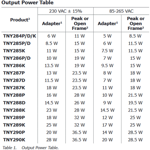
As we can see, the TNY284DG is perfect for our option, and as the construction of our SMPS is an open frame, thus it will match the output wattage. If you want to learn more about this IC. Do check out the datasheet of TNY284DG IC.
Components Required to Build the 3.3V/1.5A IoT SMPS Circuit
The list of components is very simple and you can find most of them in your local hobby store. The one unusual part that you cannot find in your local store is the flyback transformer and you need to build your own.
- Diode Bridge ABS8 - SMD
- 22uF / 400V
- SMBJ160A - SMD
- UF1JB - SMD
- 2Meg – 2 Pcs – 0805 package
- 0.068nF 250VAC
- TNY284DG
- 0.1uF / 50V – 2pcs - 0805 package
- PC817
- 1k – 0805 package
- 16R – 1pcs - 0805 package
- 680 pF – 50V - 0805 package
- TL431
- SS34A - SMD
- 680pF 50V – 0805 package
- 3300uF 16V
- 3.3uH – Drum core
- 2.2nF 250VAC
- 2k – 0805
- 6.1k – 0805
- 10R NTC (Inrush current limiter) – 10D-9
Compact 3.3V/1.5A SMPS Circuit - Schematic
The construction of this SMPS follows the basic flyback construction. This design uses the Power Integration chipset as an SMPS driver IC. The schematic of the circuit can be seen in the image given below.

Construction and Working of 3.3V/1.5A SMPS Circuit
Before going straight into building the prototype part, let’s explore the circuitry operation.
The circuit has the following sections.
- AC-DC conversion
- Driver circuitry or Switching circuit
- Under-voltage lockout protection.
- Clamp circuit
- Magnetics and galvanic isolation
- EMI Filtering
- Secondary Rectifier and snubber circuit
- Filter Section
- Feedback section
AC-DC conversion:
B1 is the diode bridge rectifier. This is an ABS8 rectifier, a 1A 800V diode bridge that will convert the Alternating current(AC) input to the High voltage DC. As we all know that after rectification from AC to DC, we need a bulk capacitor to rectify the DC ripple and it will provide a smooth DC output to the driver circuit, the 22uF 400V capacitor C1 is acting as the same filter capacitor and it will provide filtered DC output to the driver circuit as well as the Transformer.
Driver circuitry or switching circuit:
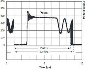
It is the main component of this SMPS. The transformer's primary side is properly controlled by the switching circuit TNY284DG. The switching frequency is 128-132 kHz whereas the default is 132Khz. Due to this high switching frequency, smaller transformers can be used.
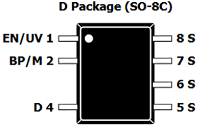
The above pinout diagram is showing TNY284DG pinouts. The Drain pin is the one that switches the transformer. The drain pin switching waveform is shown in the image given below.
The switching driver, IC1 which is TNY284DG requires a bypass capacitor for the internally generated 5.85V uses C2 a 0.1uF 16V capacitor. The TNY284DG needs to operate perfectly and this capacitor is essential for the operation.
Under-voltage lockout protection:
Under-voltage lockout is a feature that turns off the SMPS during low voltage detection. In this case, this input voltage is done using the sense resistor R1 and R2. If the input voltage is low from the required operating voltage, the SMPS goes into auto-restart mode until the voltage gets stabled.
Clamp circuit:
Inductors generate high EMF voltage that is dangerous for the driver IC and could potentially damage the device. Here, the transformer acts as a huge inductor. Thus, in each switching cycle, the transformer induces high voltage spikes due to the transformer’s leakage inductance. The Zener diode VR1 is an SMBJ160A diode, that clamps the output voltage, and the D5 which is UF1JB is an ultra-fast diode that blocks this high voltage spikes and damps them to a safe value. In this process, the DRAIN pin of the TNY284DG does not get damaged by high induced voltage.
Magnetics and galvanic isolation:
The transformer is made out of ferromagnetic material. It not only converts the high voltage AC to a low voltage ac but also provides galvanic isolation, galvanic isolation is important for safety reasons, and due to this, the low voltage circuits get isolated from the high voltage AC or DC inputs.
The transformer is made out of an EE13 Transformer Core. The detailed transformer spec is shown in the pdf given below. EE13 is used due to the small transformer size.
EMI filter:
EMI filtering is done by the C3 capacitor. C3 capacitor is a high voltage 0.068nF 250VAC capacitor which increases the circuit immunity and reduces the high EMI interference.
Secondary Rectifier and snubber circuit:
Due to the switching, the output from the transformer is also AC which needs to be rectified using a Schottky diode. In this case, we are using the SS34A Schottky diode that is available in the SMA package. This is a 40V 3A Schottky Diode. Since the output current is 1.5A, it is good to choose the current rating at least double hence, 3A is perfect for this application. This Schottky diode D6 provides DC output from the transformer which is further rectified by the large 1500uF 10V capacitor C6.
The output of the transformer provides a ringing ripple that is suppressed by the snubber circuit which is created by the low-value resistor and capacitor in series connection which is in parallel with the output rectifier. This is needed for the same reason the input of the transformer is clamped. The ringing ripple can become too high that could fail the output diode. This snubber circuit consists of a low-value resistor 16R and the low-value capacitor 680 pF. These two components, R3 and C5 create the snubber circuit in the DC output section.
Filter Section:
The filter section is created using an LC Filter configuration. It will increase the ripple rejection stability which is essential for critical application. The C is the filter capacitor C7. It is good to use a Low ESR capacitor for better ripple rejection with a value of 100uF 16V and the inductor L1 is a 3.3uH drum core inductor.
Feedback section:
The feedback section consists of three parts – Voltage divider, TL431, and optocoupler. When the driver IC first turns on, it starts the first switching cycle which got reflected in the output. The shunt regulator TL431 sense this using the voltage divider. The reference sense voltage of TL431 is 2.495V. If it senses the voltage, it turns on the optocoupler and the optocoupler provides this data to the TNY284DG. This happens for all switching cycles and if something happens, this feedback loop gets broken and the driver IC goes into the auto-restart mode. Here, TL431 is the U3 and the optocoupler is the U2, PC817. For the 3.3V output voltage, the voltage divider is created using two resistors R6 and R7.U2. The optocoupler further galvanically isolates the secondary feedback sensing portion with the primary side controller. The voltage divider is used a 2k resistor for R6 and a 6.1k resistor for R7. This divider will provide 2.495V across the TL431 when the output voltage will be 3.3V.
PCB Design for 3.3V/1.5A Compact IoT SMPS
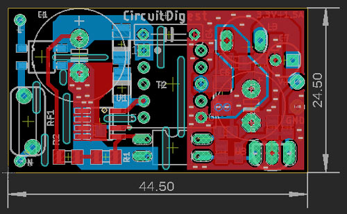
The SMPS is designed using an eagle and it is too small, 4.5 cm x 25 cm.
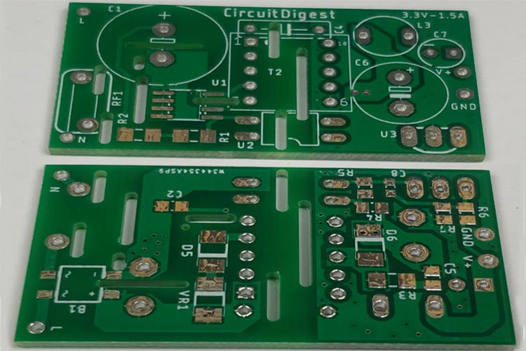
Top Side:
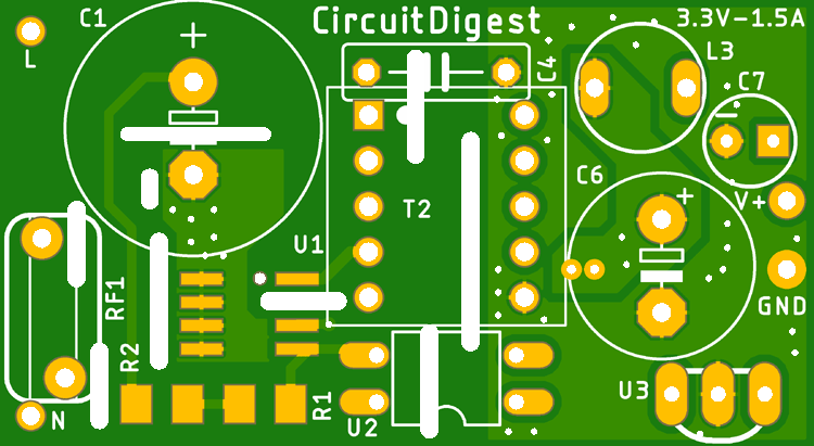
The top side is shown in the image given above. It is a double-layer PCB board with a planned thickness of 70um of copper. High thickness is required due to the small size and restricted place for creating the copper-based heatsink. The output diode and the driver IC need special thermal consideration for heat dissipation-related purposes.
Also, on the secondary side via stitching is done for better ground connectivity.
Bottom Side:
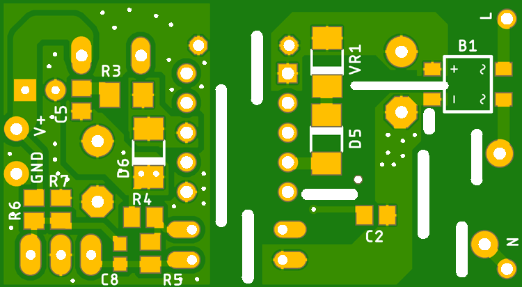
SMD components are also placed on the backside of the board for keeping the module size in a small dimension.
Ordering PCB from PCBWay
After finalizing the design, you can proceed with ordering the PCB:
Step 1: Go to https://www.pcbway.com/, sign up if this is your first time. Then, in the PCB Prototype tab, enter the dimensions of your PCB, the number of layers, and the number of PCB you require.
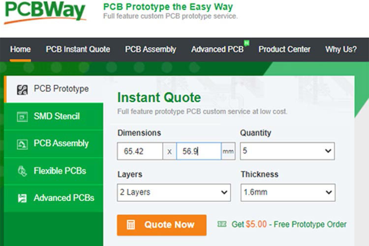
Step 2: Proceed by clicking on the ‘Quote Now’ button. You will be taken to a page where you need to set a few additional parameters like the Board type, Layers, Material for PCB, Thickness, and more. Most of them are selected by default, but if you are opting for specific parameters, you can select them here.
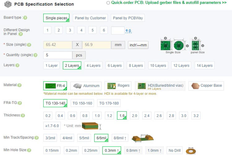
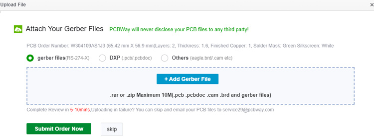
Step 3: The final step is to upload the Gerber file and proceed with the payment. To make sure the process is smooth, PCBWAY verifies if your Gerber file is valid before proceeding with the payment. This way, you can be sure that your PCB is fabrication-friendly and you will receive it as committed.
Assembling our 3.3V 1.5A SMPS Board
After a few days, we received our PCB in a neat package and the PCB quality was good as always. The top layer and the bottom layer of the board are shown below:
After making sure the tracks and footprints were correct, I proceeded with assembling the PCB. The image here shows how the completely soldered board looks like.
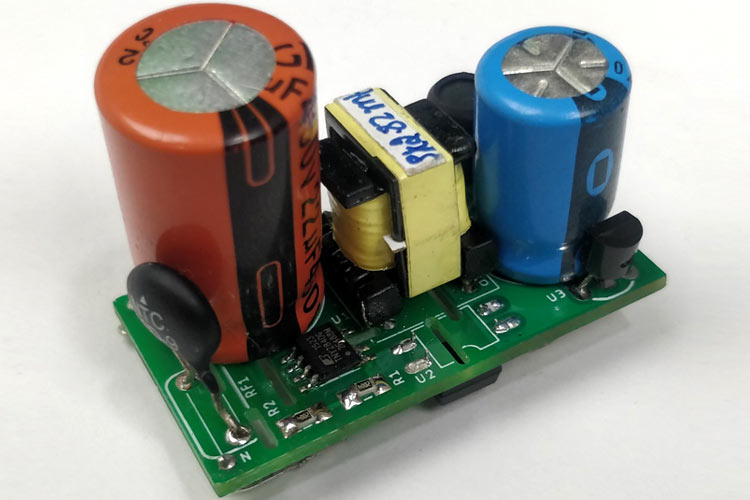
As you can see, all components are soldered properly. You might be finding it difficult to get the right transformer and inductor off the shelf, so it is better to approach a custom manufacturer. The specsheet for the transformer is already discussed above.
If you are not ready to approach a custom manufacturer, you can also build the transformer on your own. In one of our previous articles, we have shown you how you can Design your own Chopper Transformer for SMPS, you can check that out if you are interested and build the transformer using the specsheet shared.
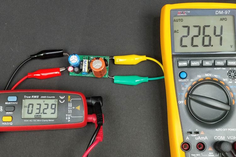
Input Voltage and Output Voltage Testing
The SMPS board is now ready for testing, I used an auto-transformer to vary the input AC voltage and used a multimeter to measure the input and output voltage from the SMPS circuit.
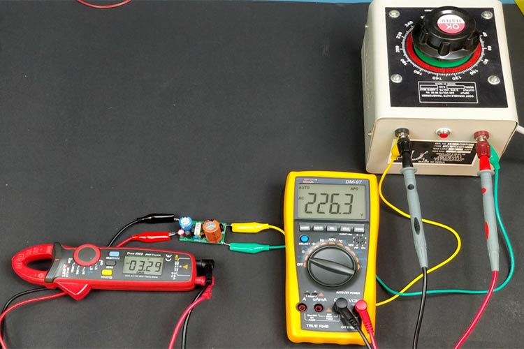
As you can see the output voltage is 3.29V, which is close to our desired 3.3V. I also varied the input AC voltage from 90V to 240V and found the output voltage to be constant at 3.3V.
You can check out the video at the bottom of this page for complete testing.
3.3V 1.5A SMPS – Load Test
We used our adjustable DC load machine to load our SMPS board and see how the output voltage holds for the different current draw. This Arduino-based Adjustable DC load machine was also built by us previously, you can check it out if you are interested. The testing set-up is shown below.
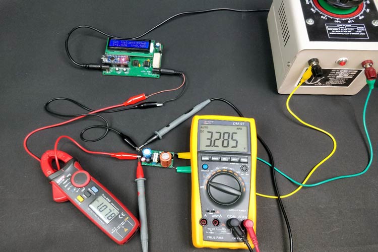
The clamp meter is used to measure the output current from our SMPS and the multimeter is used to measure the output voltage from the SMPS. As you can see, the output voltage is pretty much held onto 3.3V even at different values of current drawn.
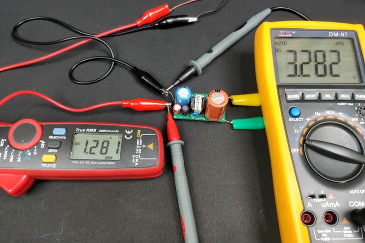
I was able to test up to 1.3A and the output voltage did not drop below 3.28V which is good. You can check out the complete testing procedure in the video linked below.
Powering NodeMCU and other Microcontrollers with our SMPS Boards
I was not able to check for ripple or noise on this board but I did try to power various microcontroller modules like this ESP8266 as shown below.
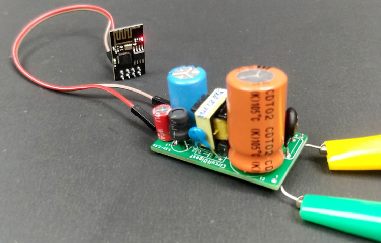
The module worked without any problem and I am sure this design would be of great use when you are making your own custom power supply for your IoT devices. Hope this tutorial was interesting and you learned something useful. The complete working can also be found in the video linked below.
If you have any questions, you can post them in the comment section below or use our technical forum to start a discussion.

Thanks you very much sir. It is a very helpful and informative for electronic student.