

An inverter is a circuit that converts Direct Current (DC) to Alternating Current (AC). A PWM inverter is a type of circuit that uses modified square waves to simulate the effects of Alternating Current (AC), which is suitable for powering most of your household appliances. I say most-of because there generally exist two types of inverters, the first type is the so-called a modified square wave inverter, as the name implies the output is a square wave rather than a sine wave, not a pure sine wave so, if you try to power AC motors or TRIACS, it will cause different problems.
The second type is called a pure sine wave inverter. So it can be used for all kinds of AC appliances without a problem. Learn more about different types of inverter here.
But in my opinion, you should not build an inverter as a DIY project. If you are asking why?, then ride along!, and in this project, I will be building a simple modified square wave PWM inverter circuit by using the popular TL494 chip and explain the pros and cons of such an inverters and at the end, we will see why not to make a modified square wave inverter circuit as a DIY project.
WARNING! This circuit is built and demonstrated for educational purposes only, and it’s absolutely not recommended to build and use this type of circuit for commercial appliances.
CAUTION! If you are making this type of circuit, please be extra careful about high voltage and voltage spikes generated by the non-sinusoidal nature of the input wave.
How does an Inverter Work?
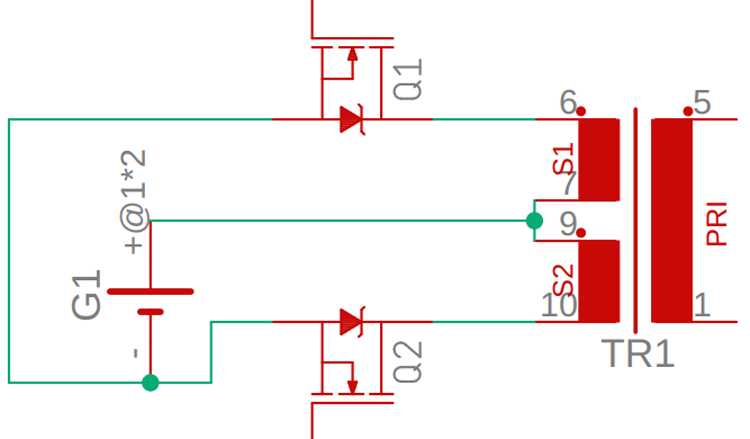
A very basic schematic of the inverter circuit is shown above. A positive voltage is connected to the middle pin of the transformer, which is acting as an input. And the two other pins are connected with the MOSFETs which are acting as switches.
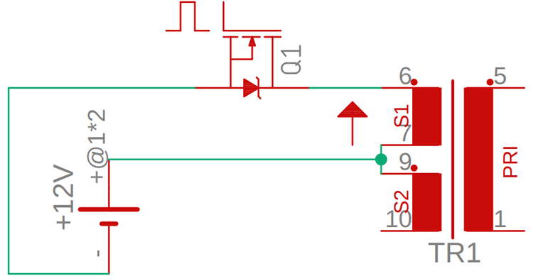
Now if we enable MOSFET Q1, by putting a voltage at the gate terminal the current will flow in one direction of the arrow as shown in the image above. Thus a Magnetic flux will also be induced in the direction of the arrow and the core of the transformer will pass the magnetic flux in the secondary coil, and we will get 220V at the output.
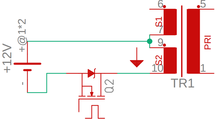
Now, if we disable the MOSFET Q1 and enable the MOSFET Q2, the current will flow in the direction of the arrow shown in the above image, thus reversing the direction of the magnetic flux in the core. Learn more about the working of MOSFET here.
Now, we all know that a transformer work by magnetic flux changes. So, turning both the MOSFETs on and off, one inverted to another and doing that 50 times in a second, will generate a nice oscillating magnetic flux inside the core of the transformer and the changing magnetic flux will induce a voltage in the secondary coil as we know by the faraday's law. And that is how the basic inverter works.
Inverter IC TL494
Now before building the circuit based upon the TL494 PWM controller, let's learn how the PWM controller TL494 works.
The TL494 IC has 8 functional blocks, which are shown and described below.
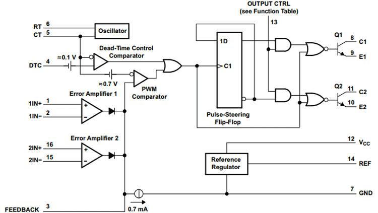
1. 5-V Reference Regulator
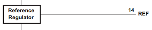
The 5V internal reference regulator output is the REF pin, which is pin-14 of the IC. The reference regulator is there to provide a stable supply for internal circuitry like the pulse-steering flip-flop, oscillator, dead-time control comparator, and PWM comparator. The regulator is also used to drive the error amplifiers which are responsible for controlling the output.
Note! The reference is internally programmed to an initial accuracy of ±5% and maintains stability over an input voltage range of 7V to 40 V. For input voltages less than 7 V, the regulator saturates within 1 V of the input and tracks it.
2. Oscillator
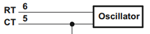
The oscillator generates and provides a sawtooth wave to the dead time controller and the PWM comparators for various control signals.
The frequency of the oscillator can be set by selecting timing components RT and CT.
The frequency of the oscillator can be calculated by the formula below
Fosc = 1/(RT * CT )
For simplicity, I have made a spreadsheet, by which you can calculate the frequency very easily.
Note! The oscillator frequency is equal to the output frequency only for single-ended applications. For push-pull applications, the output frequency is one-half of the oscillator frequency.
3. Dead-time Control Comparator
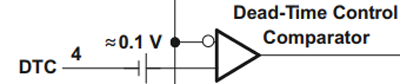
The dead time or to simply say off-time control provides the minimum dead time or off-time. The output of the dead time comparator blocks switching transistors when the voltage at the input is greater than the ramp voltage of the oscillator. Applying a voltage to the DTC pin can impose additional dead time, thus providing additional dead time from its minimum of 3% to 100% as the input voltage varies from 0 to 3V. In simple terms, we can change the Duty cycle of the output wave without tweaking the error amplifiers.
Note! An internal offset of 110 mV ensures a minimum dead time of 3% with the dead-time control input grounded.
4. Error Amplifiers
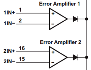
Both high-gain error amplifiers receive their bias from the VI supply rail. This permits a common-mode input voltage range from –0.3 V to 2 V less than VI. Both amplifiers behave characteristically of a single-ended single-supply amplifier, in that each output is active high only.
5. Output-Control Input
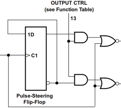
The output-control input determines whether the output transistors operate in parallel or push-pull mode. By connecting the output control pin which is pin-13 to ground sets the output transistors in parallel operation mode. But by connecting this pin to 5V-REF pin sets the output transistors in push-pull mode.
6. Output Transistors
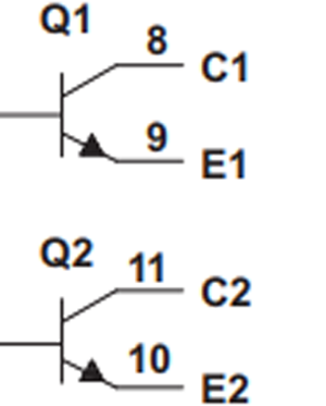
The IC has two internal output transistors which are in open-collector and open-emitter configurations, by which it can source or sink a maximum current up to 200mA.
Note! The transistors have a saturation voltage of less than 1.3 V in the common-emitter configuration and less than 2.5 V in the emitter-follower configuration.
Features
- Complete PWM Power-Control Circuitry
- Uncommitted Outputs for 200-mA Sink or Source Current
- Output Control Selects Single-Ended or Push-Pull Operation
- Internal Circuitry Prohibits Double Pulse at Either Output
- Variable Dead Time Provides Control Over Total Range
- Internal Regulator Provides a Stable 5-V
- Reference Supply With 5% Tolerance
- Circuit Architecture Allows Easy Synchronization
Note! Most of the internal schematic and operations description is taken from the datasheet and modified to some extent for better understanding.
Components Required
|
Sl.No |
Parts |
Type |
Quantity |
|
1 |
TL494 |
IC |
1 |
|
2 |
IRFZ44N |
Mosfet |
2 |
|
3 |
Screw Terminal |
Screw Terminal 5mmx2 |
1 |
|
4 |
Screw Terminal |
Screw Terminal 5mmx3 |
1 |
|
5 |
0.1uF |
Capacitor |
1 |
|
6 |
50K,1% |
Resistor |
2 |
|
7 |
560R |
Resistor |
2 |
|
8 |
10K,1% |
Resistor |
2 |
|
9 |
150K,1% |
Resistor |
1 |
|
10 |
Clad Board |
Generic 50x 50mm |
1 |
|
11 |
PSU Heat Sink |
Generic |
1 |
TL494 Inverter Circuit Schematic

TL494CN Inverter Circuit Construction
For this demonstration, the circuit is constructed on a homemade PCB, with the help of the schematic and PCB design files. Please note that if a big load is connected to the output of the transformer, a huge amount of current will flow through the PCB traces, and there's a chance that the traces will burn out. So, to prevent the PCB traces from burning out I have included some jumpers which help to increase the current flow.

Calculations
There are not many theoretical calculations for this Inverter Circuit using TL494. But there are some practical calculations which we will do in the testing of the circuit section.
To calculate the oscillator frequency following formula can be used.
Fosc = 1/(RT * CT )
Note! For simplicity, a spreadsheet is given by which you can easily calculate the oscillator frequency.
Testing the TL494 PWM Inverter Circuit
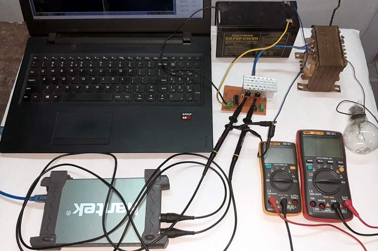
In order to test the circuit, the following setup is used.
- 12V lead-acid battery.
- A transformer which has a 6-0-6 tap and a 12-0-12 tap
- 100W incandescent light bulb as a load
- Meco 108B+TRMS Multimeter
- Meco 450B+TRMS Multimeter
- Hantek 6022BE Oscilloscope
- And the Test-PCB in which I have connected the oscilloscope probes.
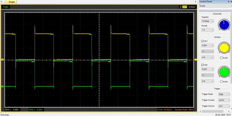
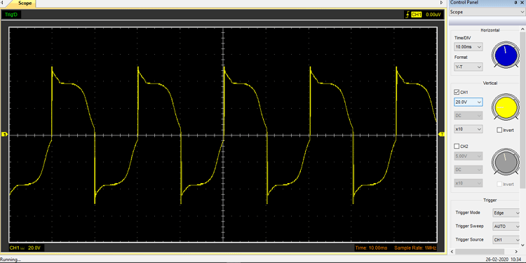
MOSFET Input
After setting up the TL494 chip, I have measured the input PWM signal to the gate of the MOSFET, as you can see in the image below.
The output waveform of the transformer without load (I have connected another secondary transformer to measure the output waveform)

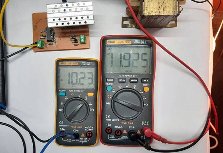
As you can see in the above image, the system draws around a wapping 12.97W without any load attached.


So from the above two images, we can easily calculate the efficiency of the inverter very easily.
The efficiency is around 65%
Which is not bad but it's also not good.
So as you can see the output voltage drops to half of what our commercial AC mains input.
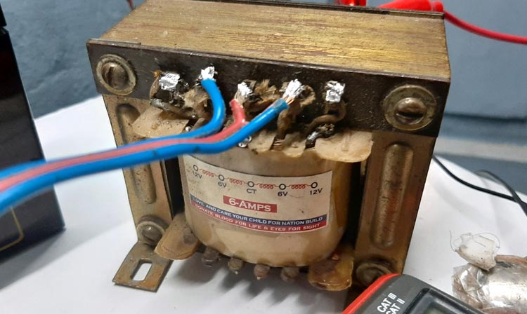
Luckily the transformer I am using contains a 6-0-6 taping, alongside 12-0-12 taping.
So, I thought why not use the 6-0-6 taping to increase the output voltage.

As you can see from the above picture the power consumption without load is 12.536W

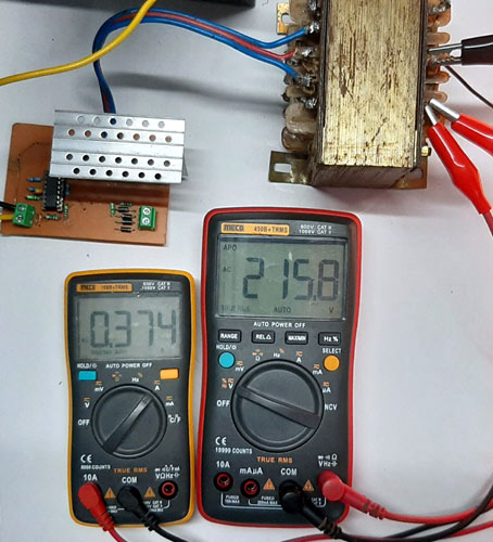
Now the output voltage of the transformer is in lethal levels
Caution! Be extra cautious when working with high voltages. This amount of voltage can certainly kill you.
Again Input power consumption when a 100W bulb is connected as a load
At this point, the puny probes of my multimeter were not sufficient enough to pass through 10.23Amps of current, so I have decided to put 1.5sqmm of wire directly into the multimeter terminals.
The input power consumption was 121.94 Watts
Again the output power consumption when a 100W bulb is connected as a load
The output power consumed by the load was 80.70W. As you can see the light bulb was glowing very brightly, that is why I put it beside my table.
So again if we calculate the efficiency, it's around 67%
And now the million-dollar question remains
Why NOT Make a Modified Square Wave Inverter Circuit as a DIY Project?
Now after viewing the above results, you must be thinking that this circuit is good enough right?
Let me tell you this is absolutely not the case at all because
First of all, efficiency is really very poor.
Depending upon the load, the output voltage, the output frequency, and the shape of the wave changes as there is no feedback frequency compensation and no LC filter at the output to clean things up.
At this moment, I am unable to measure the output spikes because the spikes will kill my oscilloscope and the connected laptop. And let me tell you there are certainly huge spikes which are being generated by the transformer which I know by watching the Afrotechmods video. This means connecting the inverter output to 6-0-6 V terminal was reaching the peak to peak voltage of over 1000V and that is life-threatening.
Now, just think about powering up a CFL lamp, a phone charger, or a 10W light bulb with this inverter, it will instantly blow up.
Many designs I have found on the internet have a high voltage capacitor at the output as a load, which reduces the voltage spikes, but that's also not going to work. As spikes of 1000V can instantly blow the capacitors. If you connect it to a laptop charger or an SMPS circuit the Metal-Oxide Varistor (MOV) inside will instantly blow up.
And with that, I can go on and on with the cons all day.
This was the reason that I do not recommend building and working with these types of circuits as it is unreliable, unprotected, and can harm you for good. Although previously, we build an inverter that is also not good enough for practical applications. Instead, I will tell you to spend a bit of money and buy a commercial inverter that has a ton of protection features.
Further Enhancement
The Only enhancement that can be done to this circuit is to completely throw it away, and modify it with a technique called SPWM (Sine Pulse Width Modulation), and add proper feedback frequency compensation and short circuit protection and more. But that is a subject for another project which is coming soon by the way.
Applications of TL494 Inverter Circuit
After reading all this if you are thinking about applications, then I will tell you in emergencies, it can be used to charge up your phone laptop and other things.
I hope you liked this article and learned something new. Keep reading, keep learning, keep building, and I will see you in the next project.

Hi. Hundred of thanks.this subject was necessary for me to progress.