
")
Most of the consumer electronic devices around us like Mobile phones, TV, Radio, Mp3 Players etc are a combination of Digital and Analog Electronics. Wherever there is wireless transmission/reception or audio signals are involved in an electronic design there we will need periodic oscillating electronic signals these signals are called as Oscillating signals and are very useful in wireless transmission or to perform timing related operations.
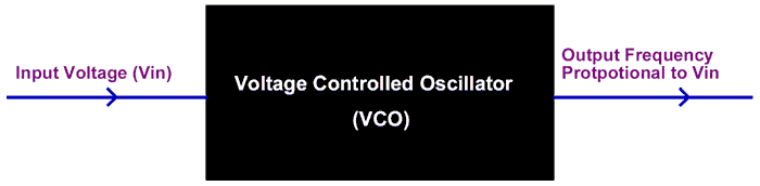
An Oscillator in electronics generally refers to a circuit which is capable of producing waveforms. This waveform can either be of Sine, triangle or even a saw tooth type. Some of the most common oscillator circuits are LC circuit, Tank circuit etc. A Voltage Controlled Oscillator is an oscillator which produces oscillating signals (waveforms) with variable frequency. The frequency of this waveform is varied by varying the magnitude of the Input voltage. For now you can imagine a Voltage Controlled Oscillator (VCO) to be a black box which takes in Voltage of variable magnitude and produces an output signal of variable frequency, and the frequency of the output signal is directly proportional to the magnitude of the input voltage. We will learn more about this black box and how to use one in our designs in this tutorial.
Working Principle of Voltage Controlled Oscillator (VCO)
There are many types of VCO circuits; a very basic one can be built by just utilising a capacitor, inductor and resistor to make a tank circuit. Also Op-Amps, Multivibrator, transistors, 555 timers can also be utilised to build oscillating circuits. Apart from that there are dedicated IC packages like LM566 LM567 etc. which can act as VCO. To understand the basic idea of a VCO let us consider a RC oscillator.
In a RC oscillator the frequency of the output wave depends on the value of the capacitor used in the circuit, since the frequency is given by the formulae
Frequency (f) = 1 / 2πRC
Hence in this case the frequency of oscillation is inversely proportional to the value of capacitance used in the circuit. So now to control the output frequency and to make it work as a VCO we have to vary the capacitance of the Capacitor based on the value of the Input voltage. This can be achieved with the help of varactor diodes. These diodes change the value of capacitance across them based on the voltage applied. A sample output graph of a VCO is shown below.
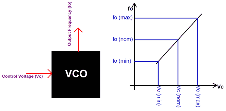
Let us assume the control voltage to be Vc and the output frequency as fo. Then under normal operating condition a nominal voltage provided to the VCO for which a nominal Frequency is produced by the VCO. As the input voltage (control voltage) is increased the output frequency increases and the vice versa is also possible.
Types of Voltage Controlled Oscillators
There are many types of VCO circuits used in different applications, but they can be broadly classified into two types based on their output voltage.
Harmonic Oscillators: If the Output waveform of the oscillator is sinusoidal then it is called as harmonic Oscillators. The RC, LC circuits and Tank circuits fall into this category. These types of oscillators are harder to implement but they better stability than the Relaxation Oscillator. Harmonic oscillators are also called as linear voltage controlled oscillator.
Relaxation Oscillator: If the output waveform of the oscillator is in sawtooth or triangular form then the oscillator is called as Relaxation Oscillator. These are comparatively easy to implement and hence most widely used. Relaxation Oscillator can further be classified as
- Emitter Coupled Voltage Controlled Oscillator
- Grounded capacitor Voltage Controlled Oscillator
- Delay based ring Voltage Controlled Oscillator
Voltage Controlled Oscillator – Practical Application
As mentioned earlier VCO can be simply construct using RC or LC pair, but in real world application no one really does that. There is some dedicated IC which has the ability to generate oscillations based on the input voltage. One such commonly used IC is the LM566 from national semiconductor.
This IC is capable of generating both triangular and square wave and the nominal frequency of this wave can be set by using an external and capacitor and a resistor. Later this frequency can also be varied in real time based on the input voltage supplied to it.
The pin diagram of the LM566 IC is shown below
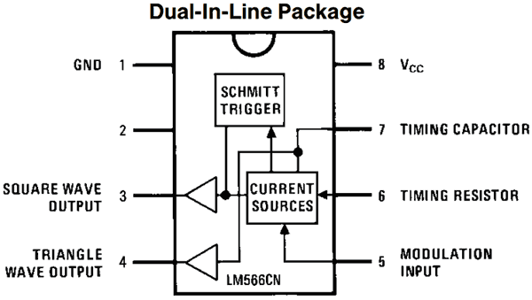
The IC can be operated either from a single supply or from a dual supply rail with an operating voltage upto 24V. The pins 3 and 4 are the output pins which gives us the Square wave and Triangle wave respectively. The Nominal frequency can be set by connecting the right value of Capacitor and Resistor to the pins 7 and 6.
The formulae to calculate the value of R and C based on the output frequency (Fo) is given by the formulae
Fo = 2.4 (Vss - Vc) / Ro+Co+Vss
Where,
Vss is the supply voltage (here 12V) and Vc is the control voltage applied to pin 5 based on whose magnitude the output frequency is controlled. (Here we have formed a potential divider using 1.5k and 10k Resistor to supply a constant voltage to pin 5). A sample circuit diagram for LM566 is shown below
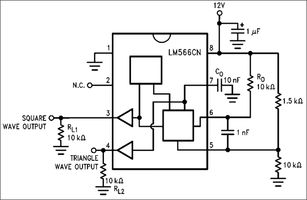
In practical applications the Resistors 1.5k and 10k can be ignored and the control voltage can be directly supplied to pin 5. You can also change the value of Ro and Co based on you required range of output frequency. Also refer the datasheet to check how linear the output frequency varies with respect to the Input control voltage. The value of output frequency is adjustable using the Control voltage (on pin 5) with a ratio of 10:1, which helps us in providing a wide range of control.
Applications of Voltage Controlled Oscillators (VCO)
- Frequency Shift Keying
- Frequency identifiers
- Keypad Tone recognizers
- Clock/Signal/Function Generators
- Used to build Phase Locked Loops.
The voltage controlled oscillator is the main function block in a Phase Locked Loop system. So let us also understand about the Phase locked Loop, why it is important and what a VCO does inside a Phase Locked Loop.
What is a Phase Locked Loop (PLL)?
Phase Locked Loop also referred as PPL, is a control system while mainly consists of three important blocks. They are Phase Detector, Low Pass Filter and Voltage controlled Oscillator. Together these three forms a control system which constantly adjusts the frequency of the output signal based on the frequency of the input signal. The block diagram of a PLL is shown below
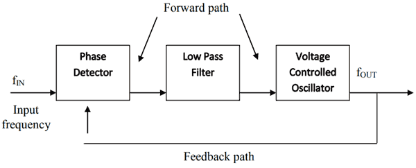
The PLL system is used in application where a high stable Frequency (fOUT) has to be obtained from an unstable frequency signal (fIN). The main function of a PLL circuit is to produce the output signal with the same frequency of the input signal. This is very important in wireless applications like Routers, RF transmission systems, Mobiles networks etc.
The Phase detector compares the Input frequency (fIN) with the output frequency (fOUT) using the feedback path provided. The difference in these two signals are compared and given in terms of a voltage value, and is referred as Error voltage signal. This voltage signal will also have some high frequency noise coupled with it, which can be filtered by using a Low pass filter. Then this voltage signal is provided to a VCO which as we already know varies the output frequency based on the voltage signal (control voltage) provided.
PLL - Practical Application
One of the commonly used PLL implement IC is the LM567. It is a tone decoder IC, meaning it listens to a particular user configured type of tone on pin 3 if that tone is received it connects the output (pin 8) to ground. So basically to listens to all the sound in available in the frequency and keeps comparing the frequency of those sound signals with a preset frequency using the PLL technique. When the frequencies match the output pin it turned low. The pin of the LM567 IC is shown below, the circuit is highly susceptible to noise so don’t be surprised if you cannot get this IC to work on a breadboard.
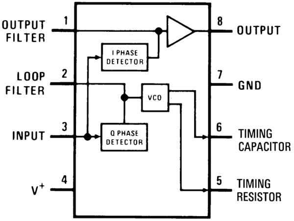
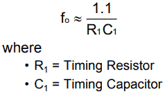
As shown in the pin out, the IC consist of a I and Q Phase detector circuit inside it. This Phase detectors check the difference between the set frequency and incoming frequency signal. External components are used to set the value of this set frequency. The IC also consists of a Filter circuit which will filter the erratic switching noise, but it requires an external capacitor connected to pin 1. The 2nd pin is used to set the bandwidth of the IC, higher the capacitance lower will be the bandwidth. The pins 5 and 6 are used to set the value of set frequency. This frequency value can be calculated by using the below formulae
The basic circuit for the LM567 IC is shown below.
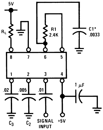
The Input Signal whose frequency has to be compared is given to the pin 3 through a filtering capacitor of value 0.01uF. This frequency is compared with the set frequency. The frequency is set using the 2.4k Resistor (R1) and 0.0033 Capacitor (C1), these values can be calculated according to your set frequency using the above discussed formulae.
When the input frequency is matched with the set frequency the output pin (pin 8) will be grounded. If otherwise this pin will remain high. Here we have used a Resistor (RL) as load, but normally it will be a Led, or buzzer as required by the design. Thus the LM567 uses the ability of VCO to compare frequencies which is very useful in audio/wireless related applications.
Hope you got a good idea about VCO’s now, if you have any doubt post them on the comment section or use the forums.
Also check:

Good and thorough explanation. pls, i want to aask if i can use LM556 for GSM jamming circuit.
Secondly, is there similar tutorial with just transistors?
Thanks