

Back in the ENIAC era, computers were more analog in nature and used very few digital ICs. Today an average Joe’s computer works with multiple voltage levels, people who had seen the SMPS of a CPU would have noticed that your computer requires ±12V, +5V and +3.3V to operate. These voltage levels are very important for a computer; a specific voltage determines the state of the signal (high or low). This high state is accepted by the computer as binary 1 and the low state as binary 0. Depending on the 0 and 1 condition computer produces data, codes, and instructions to provide required output.
Modern logic voltage levels largely vary from 1.8V to 5V. The standard logic voltages are 5V, 3.3V, 1.8V, etc. But, How does a system or controller working with 5V logic level (Example Arduino) communicate with another system that works with 3.3V (Example ESP8266) or any other different voltage level? This scenario often occurs in many designs, where there are multiple micro-controllers or sensors are used and the solution here is to use a Logic Level Converter or Logic Level Shifter. In this article we will learn more about Logic Level Converters and we will also build a simple Bi-directional Logic Level converter circuit using MOSFET which will come in handy for your circuits designs.
High-Level and Low-Level Input voltage
However, from the microprocessor or the microcontroller side, the logic voltage level value is not a fixed; it has some tolerance with it. For example, the accepted Logic High (logic 1) for 5V logic level microcontrollers is minimum 2.0V (Minimum High Level Input Voltage) to a maximum of 5.1V (Maximum High Level Input Voltage). Similarly, for logic low (logic 0) the accepted voltage value is from 0V (Minimum Low Level Input Voltage) to the maximum of 8V (Maximum Low Level Input Voltage).
Above example is true for 5V logic level microcontrollers but 3.3V and 1.8V logic level microcontrollers are also available. In such type of microcontrollers, the logic level voltage range will vary. You can get the relevant information from the datasheet of that particular controller IC. When using a voltage level converter, care should be taken that the high voltage value and low voltage value is within the limit of these parameters.
Bi-directional Logic Level Converter
Depending on the application and technical construction, two types of level shifters are available, Unidirectional Logic Level Converter and Bi-directional Logic Level Converter. In unidirectional level converters, input pins are dedicated for one voltage domain and the output pins are dedicated for the other voltage domain, but this is not the case for bi-directional level converters it can convert logic signals in both directions. For the Bi-directional level converters, each voltage domain not only has input pins but also has the output pin. For example if you provide 5.5V to input side it will convert it to 3.3V on the output side, similarly if you provide 3.3V to the output side, it will convert it to 5V on the input side.
In this tutorial, we will build a simple bi-directional level converter and will test it for High to Low conversion and Low to High conversion.
Simple Bi-directional Logic Level Converter
A simple bi-directional logic converter circuit is shown in the below image.
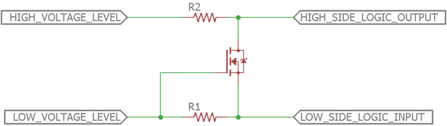
The circuit uses an n-channel MOSFET to convert the low voltage logic level to a high voltage logic level. A simple logic level converter can also be built using resistive voltage dividers but it will introduce voltage loss. MOSFET or transistor-based logic level converters are professional, reliable, and safer to integrate.
The circuit also uses two additional components, R1 and R2. Those are pull-up resistors. Due to the lowest part count, it is a cost-effective solution too. Depending on the above circuit, a simple 3.3V to 5V bi-directional logic converter will be constructed.
5V to 3.3V Level Converter using MOSFET
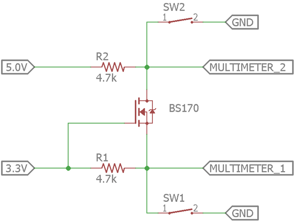
The 5V to 3.3V bi-directional logic level converter circuit can be seen in the below image -
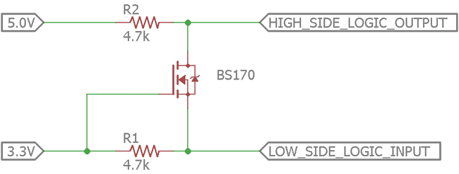
As you can see we have to provide a constant voltage of 5V and 3.3V to the resistors R1 and R2. The pins Low_side_Logic_Input and High_Side_Logic_Input can be interchangeably used as Input and Output pins.
The components used in the above circuit are
R1 - 4.7k
R2 - 4.7k
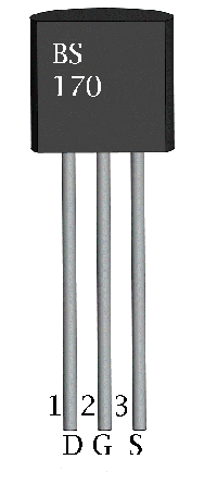
Q1 - BS170 (N channel MOSFET).
Both resistors are 1% tolerant. Resistors with 5% tolerance will also work. The pinouts of BS170 MOSFET can be seen in the below image which is in the order Drain, Gate and Source.
The circuit construction consists of two pull up resistors 4.7k each. Drain and the source pin of MOSFET are pulled up to the desired voltage level (in this case 5V and 3.3V) for the low to high or high to low logic conversion. You can also use any value between 1k to 10k for R1 and R2 since they acts only as pull up resistors.
For the perfect working state, there are two conditions that need to be met while constructing the circuit. The first condition is, the low level logic voltage (3.3V in this case) requires to be connected with the MOSFET’s source and the high level logic voltage (5V in this case) must be connected to the drain pin of the MOSFET. The second condition is, the gate of the MOSFET needs to be connected to the low voltage supply (3.3V in this case).
Simulation of Bi-Directional Logic Level Converter
The complete working of the logic level shifter circuit can be understood by using simulation results. As you can see in the below GIF image, during high level to low level logic conversion the Logic input pin is shifted between 5V and 0V (ground) and the logic output is obtained as 3.3V and 0V.

Similarly during the low level to high level conversion the Logic input is between 3.3V and 0V is converted into Logic output of 5V and 0V as shown in the below GIF image.

Logic Level Converter Circuit Working
After fulfilling those two conditions, the circuit works in three states. The states are described below.
- When the low side is in logic 1 or high state (3.3V).
- When the low side is in logic 0 or low state (0V).
- When the High side changes the state from 1 to 0 or high to low (5V to 0V)
When the low side is high, that means the source voltage of the MOSFET is 3.3V, the MOSFET does not conduct due to the Vgs threshold point of the MOSFET is not achieved. At this point the gate of the MOSFET is 3.3V and the source of the MOSFET is also 3.3V. Therefore, Vgs is 0V. The MOSFET is off. Logic 1 or high state of the low side input reflects on the drain side of the MOSFET as a 5V output via the pullup resistor R2.
In this situation, if the low side of the MOSFET changes its state from high to low, the MOSFET starts to conduct. The source is in logic 0, hence the high side also became 0.
Those above two conditions successfully convert low voltage logic state to a high voltage logic state.
Another working state is when the high side of the MOSFET changes its state from high to low. It is the time when the drain substrate diode starts to conduct. The MOSFET low side is pulled down to a low voltage level until the Vgs cross the threshold point. The bus line of both low and high voltage section became low at the same voltage level.
Switching speed of the Converter
Another important parameter to consider when designing a logic level converter is the Transition speed. Since most logic converters will be used between communication buses like USART, I2C etc it is important for the logic converter to switch fast enough (transition speed) to match up with the baud rate of the communication lines.
The transition speed is the same as the switching speed of the MOSFET. Hence in our case according to the BS170 datasheet, the turn-on time of the MOSFET and turn-off time of the MOSFET is stated below. Hence it is important to select the right MOSFET for your logic level converter design.
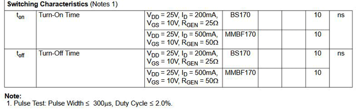
So our MOSFET here requires 10nS to turn on and 10nS to turn off, meaning it can turn on and off 10,00,000 times in one second. Assuming that our communication line is operating at a speed of (baud rate) 115200 bits per second, then it means it turns and off only 1,15,200 in one second. So we can very well use our device for high baud rate communication as well.
Testing your Logic Converter
The following components and tools are required to test the circuit -
- Power supply with two different voltage output.
- Two multimeters.
- Two tactile switches.
- Few wires for connection.
The schematic is modified to test the circuit.
In the above schematic, two additional tactile switches are introduced. Also, a multimeter is attached to check the logic transition. By pressing SW1, the low side of the MOSFET changes its state from high to low and the logic level converter is working as a low voltage to high voltage logic level converter.
On the other hand, by pressing SW2, high side of the MOSFET changes its state from high to low and the logic level converter is working as a high voltage to low voltage logic level converter.
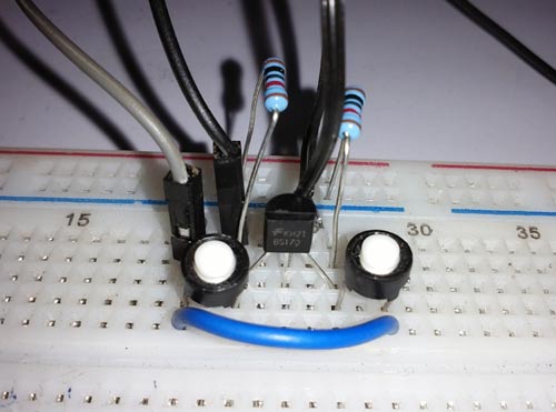
The circuit is constructed in a breadboard and tested.
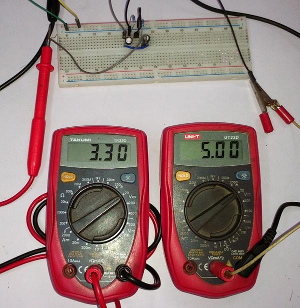
The above picture is showing the logic state across both sides of the MOSFET. Both are in Logic 1 state.
The full working video can be seen in the below video.
Limitations of Logic Level Converter
The circuit certainly has some limitations. The limitations are highly dependent on the selection of the MOSFET. The maximum voltage and drain current can be used in this circuit is dependent on the MOSFET's specification. Also, the minimum logic voltage is 1.8V. Less than 1.8V logic voltage will not work properly due to the Vgs limitation of the MOSFET. For lower voltage than 1.8V, dedicated logic level converters can be used.
Importance and Applications
As discussed in the introductory part, incompatible voltage level in digital electronics is a problem for interfacing and data transmission. Therefore, a level converter or level shifter is required to overcome the voltage level related errors in the circuitry.
Due to the availability of wide range logic level circuits in the electronics market and also for the different voltage level microcontrollers, logic level shifter has an incredible use case. Several peripherals and legacy devices which work based on I2C, UART, or audio codec, need level converters for communication purposes with a microcontroller.
Popular Logic Level Converter ICs
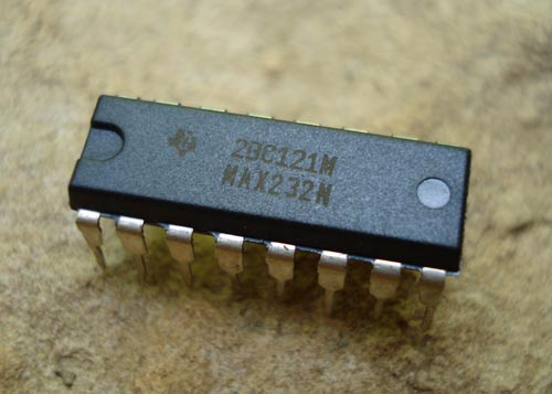
There are lots of manufacturers provide integrated solutions for logic level conversion. One of the popular IC is MAX232. It is one of the most common logic level converters IC which converts microcontroller logic voltage 5V to 12V. RS232 port is used to communicate between computers with a microcontroller and requires +/-12V. We have already used MAX232 with PIC and few other microcontrollers earlier to interface a microcontroller with computer.
There are different requirements also exist depending on the very low voltage level conversion, conversion speed, space, cost, etc.
SN74AX is also a popular series of bi-directional voltage level converter by Texas Instruments. There are lots of ICs in this segment which offers a single bit to 4-bit supply bus transition along with additional features.
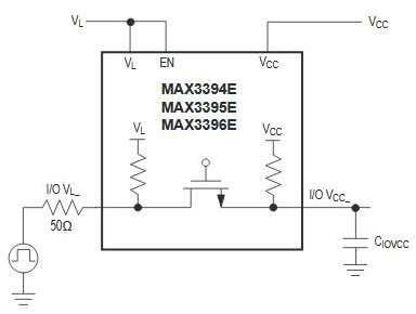
Another popular bi-directional logic level converter IC is MAX3394E from Maxim Integrated. It uses the same conversion topology using MOSFET. The pin diagram can be seen in the below image. The converter supports separate enable pin that can be controlled using microcontrollers which is an added feature.
The above internal construction is showing the same MOSFET topology but with P-channel configuration. It has lots of extra added feature such as 15kV ESD protection on I/O and VCC lines. The typical schematic can be seen in the below image.
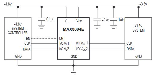
The above schematic is showing a circuit which is converting the 1.8V logic level to a 3.3V logic level and vice-versa. System controller that can be any microcontroller unit is also controlling the EN pin.
So, this is all about Bi-directional logic level conversion circuit and working.
Excellent presentation and a very useful circuit. I substituted a low on-threshold SOT-23 N-Ch MOSFET for the BS170 for use in my SMT board.
In the "High Level to Low Level Converter" simulation, you show that applying 0V at the input causes 0V to appear at the output. Why is this the case? Isn't that an anhancement mode FET, and so wouldn't it be turned OFF when Vgs = 0V (i.e. 3.3V - 3.3V)?
The reverse case ("Low level to high level converter") makes perfect sense to me, as Vgs = 3.3V, and so the FET turns ON.
sir is there any option to level shift 24V signal to 12V signal
and also i need level shifter from 12V to 5V can u please reply if u have any idea how to achieve it

Excellent presentation and quite useful. I substituted a SOT-23 N-Ch MOSFET for the