

A crude way to power your DC circuits with AC mains is to use a step-down transformer for stepping down the 230V mains voltage and adding a couple of diodes as a bridge rectifier. But due to the huge space size and other drawbacks, it cannot be used for all purposes. Another most popular and professional way is to use Switch Mode Power Supply Circuits for converting your AC mains into a wide range of DC voltage as required, almost every consumer electronics from normal 12V adapter to a Laptop Charger has a SMPS circuit to provide the required DC output power.
At circuitdigest, we have already built few popular SMPS circuits for different ratings, namely the 12V 1A Viper 22A SMPS, 5V 2A SMPS, and 12V 1A SMPS circuit each of which can be used for different applications. This time, we will build a SMPS that can be used for general purposes and has a simple module shape to be used in space-related situations. Nowadays, the Internet of Things uses various wifi-based processors like NodeMCU, ESP32, and ESP12E, etc. which operate on 5V or 3.3V. These modules are highly compact and hence to power these boards, it makes sense to use smaller SMPS circuits that can go on the same board, instead of using a separate SMPS circuit. Hence in this article, we will learn how to build a SMPS circuit that can either output 5V or 3.3V (hardware configurable using jumper), the circuit design and PCB layout is also provided, so you can simply port this into your existing design. Here our PCB boards are manufactured by PCBGoGo, a china based low cost high quality PCB prototype and PCB assembly service company.
The rating of the SMPS is 5V or 3.3V 1.5A as most of the development board uses 5V or 3.3V logic level voltages and 1.5A should be good enough for most of the IoT based applications. But do note that this SMPS does not have any filters in the input section to reduce size and cost. Therefore, this SMPS can be only used for powering microcontroller boards or charging purposes. Make sure that it will be covered from the user's reach when in operation.
Warning: Working with SMPS circuits can be dangerous as it involves AC mains voltage which is potentially lethal. Do not attempt to build this if you have no experience working with AC mains. Always stay cautious with live wires and charged capacitors, use protective tools and supervision if required. You have been warned!!
5V/3.3V SMPS Board Specifications
The SMPS will have the following specifications.
- 85VAC to 230VAC input.
- 5V or 3.3V selectable 2A output.
- Open frame construction
- Short circuit and Overvoltage protection
- Small size with low-cost features.
Materials Required for SMPS Circuit (BOM)
- Fuse 1A 250VAC Slow Blow
- Diode Bridge DB107
- 10uF / 400V
- P6KE Diode
- UF4007
- 2Meg – 2 Pcs – 0805 package
- 2.2nF 250VAC
- TNY284DG
- 10uF / 16V – 0805 package
- PC817
- 1k – 0805 package
- 22R – 2pcs - 0805 package
- 100 nF – 0805 package
- TL431
- SR360
- 470pF 100V – 0805 package
- 1000uF 16V
- 3.3uH – Drum core
- 2.2nF 250VAC
Note: All parts were selected to be easily available for designers. The SMPS transformer has to be custom build using this datasheet. You can either use a vendor to built one or design and wind your SMPS transformer using the link.
This SMPS is designed using power integration IC TNY284DG. This SMPS Diver IC is best suitable for this SMPS as the IC is available in SMD package as well as the wattage is suitable for the purpose. The below image is showing the wattage specification of TNY284DG.
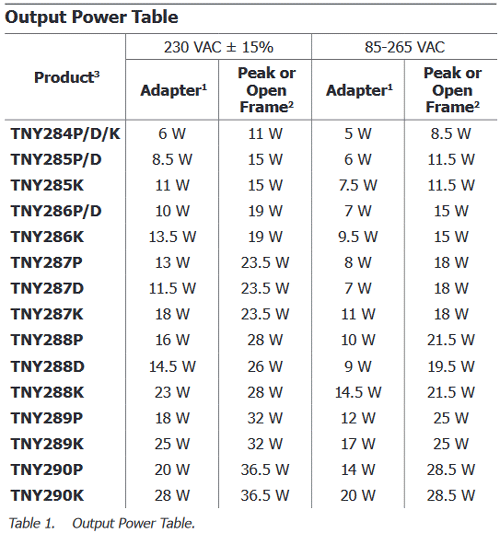
As we can see, TNY284DG is perfect for our option. As the construction is an open frame, it will match the output wattage of 8.5W. Meaning it can easily provide 1.5A at 5V.
5V/3.3V SMPS Circuit Diagram
Construction of this SMPS is pretty simple and straight forward. This design uses the Power Integration chipset as a SMPS driver IC. The schematic of the circuit can be seen in the below image-

Construction and Working
Before going straight into building the prototype part, let’s explore the circuitry operation. The circuit has the following sections-
- Input Protection
- AC-DC conversion
- Driver circuitry or Switching circuit
- Under-voltage lockout protection.
- Clamp circuit
- Magnetics and galvanic isolation
- EMI Filtering
- Secondary Rectifier and snubber circuit
- Filter Section
- Feedback section.
Input Protection
F1 is a slow blow fuse that will protect the SMPS from high load and fault conditions. The SMPS input section does not use any EMI filter considerations. This is a 1A 250VAC slow blow fuse and that will protect the SMPS in fault conditions. However, this fuse can be changed to a glass fuse. You can also check out the article on different types of fuse.
AC-DC Conversion
B1 is the diode bridge rectifier. This is DB107, a 1A 700V diode bridge. This will convert the AC input to the DC voltage. Additionally, the 10uF 400V capacitor will be essential for rectifying the DC ripple and it will provide a smooth DC output to the driver circuit as well as the Transformer.
Driver Circuitry or Switching Circuit
It is the main component of this SMPS. The transformer's primary side is properly controlled by the switching circuit TNY284DG. The switching frequency is 120-132 kHz. Due to this high switching frequency, smaller transformers can be used.

The above pinout diagram is showing TNY284DG pinouts. The switching driver IC1 which is TNY284DG uses C2 a 10uF 16V capacitor. This capacitor provides a smooth DC output to the internal circuit of TNY284DG.
Under-Voltage Lockout Protection.
Under-voltage lockout protection is done by the sense resistor R1 and R2. It is used when the SMPS goes into the auto-restart mode and senses the line voltage. This Resistor detects whether the input AC voltage is within the range or not.
Clamp Circuit
The transformer acts as a huge inductor. Therefore, in each switching cycle, the transformer induces high voltage spikes due to the transformer’s leakage inductor. The Zener diode D1 which is a P6KE160 diode, clamp the output voltage circuit and the D2 which is UF4007, an Ultra-Fast diode blocks this high voltage spikes and damp it to a safe value which is beneficial to save the DRAIN pin of the TNY284DG.
Magnetics and Galvanic Isolation
The transformer is ferromagnetic and it not only converts the high voltage AC to a low voltage ac but also provides galvanic isolation. The transformer is an EE16 Transformer. The detailed transformer specification can be seen in the transformer datasheet that was shared earlier in the materials required section.
EMI Filter
EMI filtering is done by the C3 capacitor. C3 capacitor is a high voltage 2.2nF 250VAC capacitor, which increases the circuit immunity and reduces the high EMI interference.
Secondary Rectifier and Snubber Circuit
The output from the transformer is rectified using a Schottky diode SR360. This is a 60V 3A Diode. This Schottky diode D3 provides DC output from the transformer which is further rectified by the large 1000uF 16V capacitor C6.
The output of the transformer provides a ringing ripple that is suppressed by the snubber circuit which is created by the low-value resistor and capacitor in series connection which is in parallel with the output rectifier. The low-value resistor is 22R and the low-value capacitor is 470 pF. These two components R8 and C5 create the snubber circuit in the DC output section.
Filter Section
The filter section is created using an LC configuration. The C is the filter capacitor C6. It is a Low ESR capacitor for better ripple rejection with a value of 100uF 16V and the inductor L1 is 3.3uH drum core inductor.
Feedback Section
The output voltage is sensed by the U1 TL431 by a voltage divider. Therefore, whenever the voltage divider produces a perfect voltage, the TL431 turns on an opt coupler which is PC817, denoted as OK1.
As there are two selectable voltage operation 3.3V and 5V, there are two voltage dividers created using three resistors R3, R4, and R5. R5 is common for all two dividers but the R3 and R4 are changeable using a jumper. After sensing the line, U1, the optocoupler is controlled which further triggers the TNY284DG and galvanically isolates the secondary feedback sensing portion with the primary side controller.
During the first power-up, as this is a flyback configuration, the driver turns on switching and waits for the response from the optocoupler. If everything is normal, the driver continues the switching, otherwise skip the switching cycles unless everything became normal.
Designing Our SMPS PCB
Once the circuit is finalized, you can test it on a perf board and then start with your PCB design. We have used eagle to design our PCB, you can check out the layout image below. You can also download the design files from the below link.
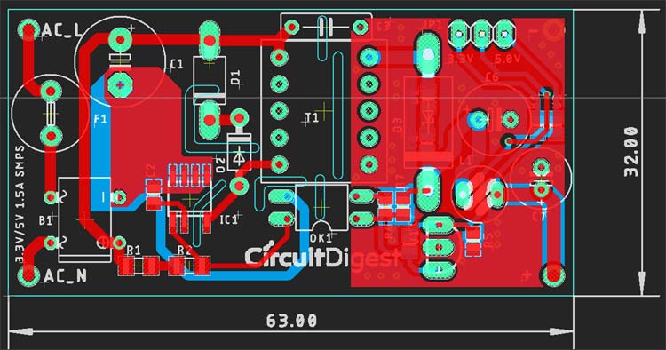
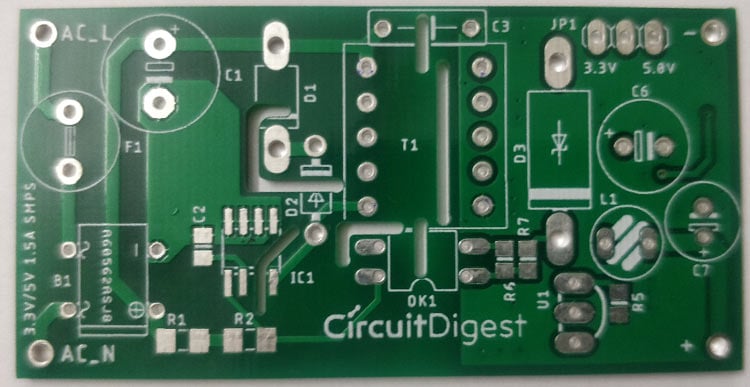
As you can see the board size is 63mm for 32mm, which is a decently small size. The components are placed at a safe distance to ensure safe operation. The top side and bottom side of our PCB are shown in the below image. It is a double layer PCB board with a planned thickness of 35um of copper. The output diode and the driver IC needs special thermal consideration for heat dissipation related purposes. Also, on the secondary side via stitching is done for better ground connectivity.
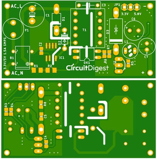
You can also notice that few SMD components are placed in the backside of the board for keeping the module size in a small dimension. There are few design considerations which you have to follow if you are designing your SMPS PCB, check out this article on SMPS PCB design Layout Guide to know more.
Fabricating PCB for 12v 1A SMPS Circuit
Now we understand how the schematics work, we can proceed with building the PCB for our SMPS. Since this is a SMPS circuit, a PCB is recommended as it could deal with noise and isolation problems. The PCB layout for the above circuit is also available for download as Gerber from the link.
Now our design is ready, it is time to get them fabricated using the Gerber file. To get the PCB done from PCBGOGO is quite easy, simply follow the steps below-
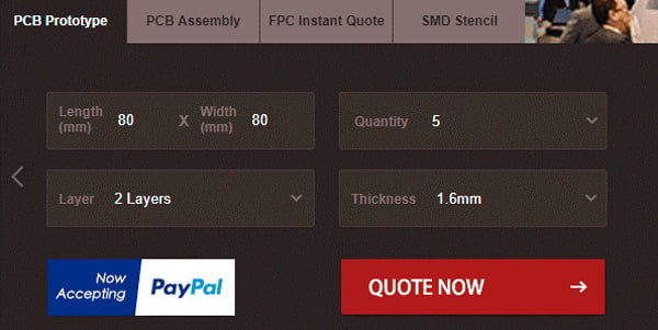
Step 1: Get into www.pcbgogo.com, sign up if this is your first time. Then in the PCB Prototype tab, enter the dimensions of your PCB, the number of layers, and the number of PCB you require. Assuming the PCB is 80cm×80cm, you can set the dimensions as shown below.
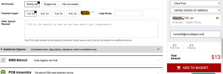
Step 2: Proceed by clicking on the Quote Now button. You will be taken to a page where to set a few additional parameters if required like the material used track spacing, etc. But mostly the default values will work fine. The only thing that we have to consider here is the price and time. As you can see the Build Time is only 2-3 days and it just costs only $5 for our PCB. You can then select a preferred shipping method based on your requirement.
Step 3: The final step is to upload the Gerber file and proceed with the payment. To make sure the process is smooth, PCBGOGO verifies if your Gerber file is valid before proceeding with the payment. This way, you can sure that your PCB is fabrication friendly and will reach you as committed.
Assembling the PCB
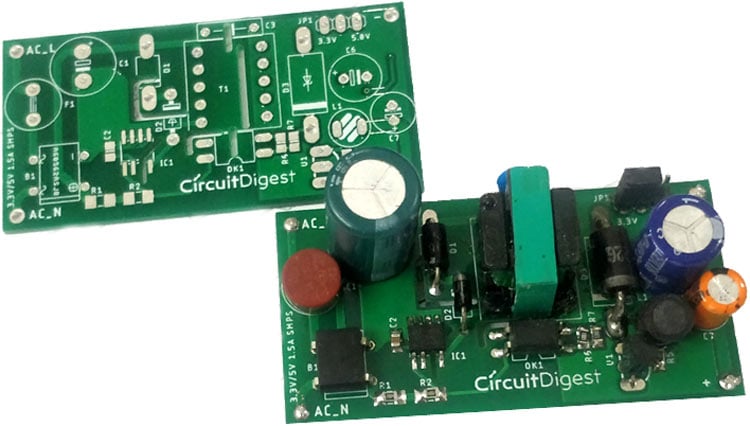
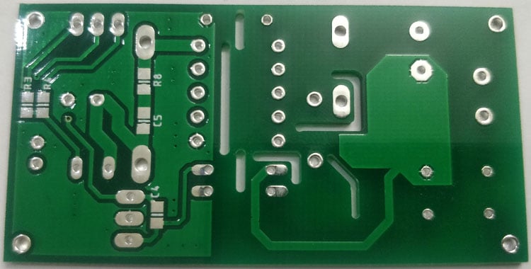
After the board was ordered, it reached me after some days through courier in a neatly labeled well-packed box, and like always the quality of the PCB was awesome. The PCB that was received by me is shown below. As you see both the top and bottom layer has turned out as expected.
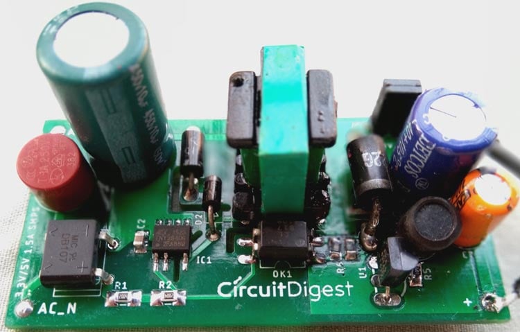
The vias and pads were all in the right size. It took me around 15 minutes to assemble to PCB board to a working circuit. The assembled board is shown below.
Testing our 5V/3.3V SMPS Circuit
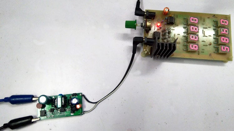
Components and the testing infrastructure was provided by Iquesters Solutions. However, the Transformer is handmade, you can also build your own SMPS transformer. Here for testing purposes, the transformer is made for 1A. One can use the proper turns ratio for 1.5A transformer as per the given transformer specifications. Our SMPS board looks like this when the assembling is done.
Now to test our SMPS board, I will be powring it using a Variac and use an Electronic DC load to adjust the output current. The below image shows my old Adjustable DC load set-up connected to our SMPS board. You can test it with any load of your choice, but using an Adjustable DC load will help you evaluate your power supply boards. You can also easily build your own Arduino based Adjustable Electronic DC Load by following this link.
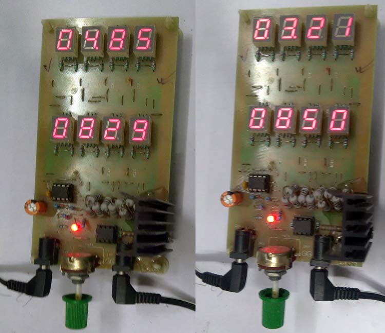
As you can see in the below image, I tested our SMPS circuit for both 5V and 3.3V by changing the jumper pin. The output current was tested for up to 850mA but you can also go till 1.5A based on your transformer design.
For more info about the testing and construction, kindly check out the video link below. I hope you enjoyed the article and learned something useful. If you have any questions, please leave them in the comment section below or use our forums.
Comments
Yes, all values mentioned in the circuit diagram is correct and you can follow the same
Would it be at all possible to get the CAD file? And also what design program was used?
Have some parts that are of other dimensions then that of your PCB.
hello, what is the transformer output and input voltage voltage? Let's calculate it according to how many volts and find it. Is it okay if we do it like the winding on 2 amps?
Hi sir, this is Hrushi I have doubt about transformer coil turns, can you help me with that?

All your work are interesting
please is there assurance that all the component values are current