

Darlington transistor is invented in 1953, by a US electrical engineer and inventor, Sidney Darlington.
Darlington transistor uses two standard BJT (Bi-polar junction transistor) transistors which are connected together. Darlington transistor connected in a configuration where one of transistor’s emitter provides biased current to the other transistor’s base.
Darlington Transistor Pair and its Configuration:
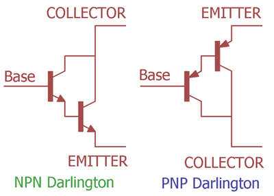
If we see the Darlington Transistor’s symbol we can clearly see how two transistors are connected. In the below images, two type of Darlington transistor are shown. On the left side it is NPN Darlington and on the other side it is PNP Darlington. We can see NPN Darlington consist two NPN transistors, and PNP Darlington consist two PNP transistors. The first transistor’s emitter is directly connected across the base of other transistor, also the collector of the two transistors are connected together. This configuration is used for both NPN and PNP Darlington transistors. In this configuration, the pair or the Darlington transistor produces much higher gain and large amplification capabilities.
A normal BJT transistor (NPN or PNP) can operate between two states, ON and OFF. We need to provide current to the base which controls the collector current. When we provide enough current to the base, the BJT enters in saturation mode and the current flows from collector to emitter. This collector current is directly proportional with the base current. The ratio of base current and collector current is called transistor’s current gain which is denoted as Beta (β). In typical BJT transistor the current gain is limited depending on the transistor specification. But in some cases the application needs more current gain that a single BJT transistor couldn’t provide. The Darlington pair is perfect for the application where high current gain is needed.
Cross Configuration:
However, the configuration shown in the above image, uses either two PNP or two NPN, there are other Darlington configuration or the cross configuration is also available, where a PNP is used with NPN, or a NPN is used with PNP. This type of cross configuration is called as Sziklai Darlington pair configuration or Push-Pull configuration.
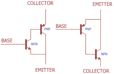
In the above image the Sziklai Darlington pairs are shown. This configuration produces less heat and has advantages about response time. We will discuss about it later. It is used for class AB amplifier or where the Push-Pull topologies are needed.
Here are few projects where we used the Darlington Transistors:
- Generating Tones by Tapping Fingers using Arduino
- Simple Lie Detector Circuit using Transistors
- Long Range IR Transmitter Circuit
- Line Follower Robot using Arduino
Darlington Transistor Pair Current Gain Calculation:
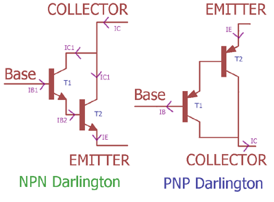
In the below image we can see two PNP or two NPN transistors are connected together.
The overall current gain of the Darlington pair will be-
Current gain (hFE) = First transistor gain (hFE1) * Second transistor gain (hFE2)
In the above image, two NPN transistors created a NPN Darlington configuration. The two NPN transistors T1 and T2 are connected together in an order where, T1 and T2’s collectors are connected. The first transistor T1 providing the required base current (IB2) to the second transistor T2’s base. So, the base current IB1, which is controlling the T1 is controlling the current flow at T2’s base.
So, the total current gain (β) is achieve, when the collector current is
β * IB as hFE = fFE1 * hFE2
As two transistors collector is connected together, Total Collector current (IC) = IC1 + IC2
Now as discussed above, we get the Collector current β * IB1
In this situation, the current gain is unity or greater than one.
Let’s see how the current gain is the multiplication of the two transistor’s current gain.
IB2 is controlled by the emitter current of T1, which is IE1. IE1 is directly connected across T2. So, IB2 and IE1 are same.
IB2 = IE1.
We can change this relationship further with
IC1 + IB1
Changing the IC1 as we did previously, we get
β1IB1 + IB1
IB1 (β1 + 1)
Now as previously, we have seen that
IC =  β1IB1 + β2IB2
As, IB2 or IE2 = IB1 (β1 + 1)
IC = β1IB1 + β2 IB1 (β1 + 1)
IC = β1IB1 + β2 IB1 β1 + β2 IB1
IC = {β1 +(β1 + β2) + β2}
So, the total collector current IC is a combinational gain of individual transistors gain.
Darlington Transistor Example:
A 60W load with 15V input voltage needs to be switched using two NPN transistors, creating a Darlington pair. The first Transistor gain will be 30 and the second transistor gain will be 95. We will calculate the base current for switching the load.
As we know, when the load will be switched on, the collector current will be the load current. As per the power law, the collector current (IC) or the Load current (IL) will be
IL = IC = Power / Voltage = 60 / 15 = 4Amps
As the base current gain for the first transistor will be 30 and for the second transistor will be 95 (β1 = 30 and β2 = 95) we can calculate the base current with the following equation –
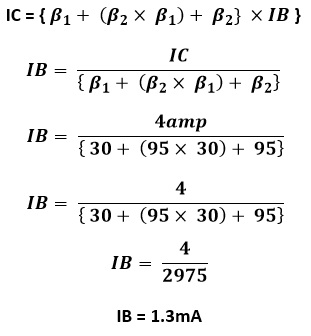
So, if we apply 1.3mA of current across the first transistor base, the Load will switch “ON” and if we apply 0 mA current or grounded the base the load will be switched “OFF”.
Darlington Transistor Application:
The application of Darlington transistor is same as normal BJT Transistor.
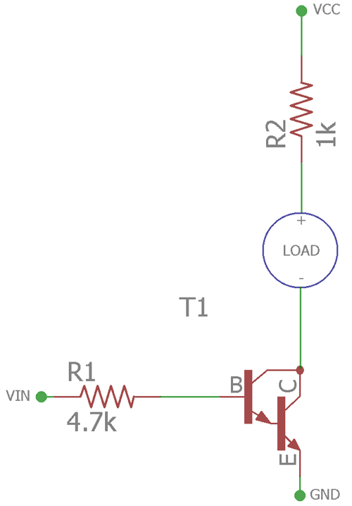
In the above image the NPN Darlington transistor is used for switching the load. The load can be anything from Inductive or Resistive load. The Base resistor R1 is providing the Base current to the NPN Darlington transistor. The R2 resistor is to limit the current to the load. It’s applicable for specific loads that need current limiting in stable operation. As the example suggests that the base current required very low, it can be switched from Microcontroller or Digital logics units easily. But when the Darlington pair is in saturated region or fully on condition, there are voltage drop across base and emitter. It is a main disadvantage for a Darlington pair. The voltage drops range from .3V to 1.2v. Due to this voltage drop the Darlington transistor get hotter when in fully on mode and supplying current to the load. Also, due to the configuration the second resistor is turned on by the first resistor, the Darlington Transistor produce slower response time. In such case Sziklai configuration provide advantage over the response time and thermal performance.
A popular NPN Darlington transistor is BC517.
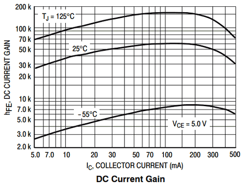
As per the datasheet of BC517, the above graph provides DC current gain of BC517. Three curves from lower to higher respectively are providing information about the ambient temperature. If we see the 25 degree ambient temperature curve, the DC current gain is maximum when collector current is around 150mA.
What is an Identical Darlington Transistor?
Identical Darlington Transistor has two identical pair with exactly same specification with the same current gain for each one. That means the current gain of the first transistor β1 is same as second transistors current gain β2.
Using the collector current formula the current gain of the Identical Transistor will be-
IC = {{β1 + (β2* β1) + β2} *IB}
IC = {{β1 + (β2* β1) + β1} *IB}
β2 = IB / IC
The current gain will be much higher. NPN Darlington pair examples are TIP120, TIP121, TIP122, BC517 and PNP Darlington pair examples are BC516, BC878, and TIP125.
Darlington Transistor IC:
Darlington pair allows users to drive more power applications by few milliamp of current source from micro controller or low current sources.
ULN2003 is a chip widely used in electronics which provide high current Darlington arrays with seven open – collector output. The ULN family consists ULN2002A, ULN2003A, ULN2004A, three different variants in multiple package options. The ULN2003 is widely used variant in ULN series. This Device includes suppression diodes inside the integrated circuit, which is an additional feature to driving inductive load using this.
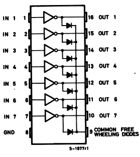
This is the internal structure of the ULN2003 IC. It is 16pin dip package. As we can see the input and output pin are exactly opposite, due to that it is easier for connecting the IC and making the PCB design more simplistic.
There are seven open collector pins are available. One additional pin is also available which is useful for inductive load related application, it can be motors, solenoids, relays, which needs freewheeling diodes, we can make the connection using that pin.
The input pins are compatible to use with TTL or CMOS, on the other side the output pins are capable to sink high currents. As per the datasheet, the Darlington pairs are capable to sink 500mA of current and can tolerate 600mA of peak current.
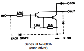
In the upper image the actual Darlington array connection is shown for the each driver. It is used in seven drivers, each driver consist this circuit.
When the input pins of ULN2003, from pin 1 to pin 7, is provided with High, the output will be low and it will sink current through it. And when we provide Low in input pin the output will be in high impedance state, and it will not sink current. The pin 9 is used for freewheel diode; it should always be connected to the VCC, when switching any inductive load using ULN series. We can also drive more current applications by paralleling two pair’s inputs and outputs, like we can connect pin 1 with pin 2 and on the other hand can connect pin 16 and 15 and parallel two Darlington pairs for driving higher current loads.
ULN2003 is also used to drive stepper motors with Microcontrollers.
Switching a Motor using ULN2003 IC:
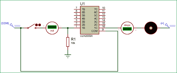
In this video the motor is connected across an open collector output pin, on the other hand the input, we are providing approx 500nA (.5mA) current and controlling 380mA of current across the motor. This is how small amount of base current can control much higher collector current in Darlington Transistor.
Also, as Motor is used, the pin 9 is connected across VCC to provide freewheeling protection.
The resistor is providing low pull up, making the input LOW when no current flow is coming from the source, which makes the output high impedance stopping the motor. The reverse will happen when additional current is applied across the input pin.
