

Anyone who deals with electronics will have come across waveform generator circuits like rectangular waveform generator, square wave generator, pulse wave generator, etc. Similarly, Bootstrap Sweep Circuit is a sawtooth waveform generator. Generally, the Bootstrap Sweep circuit is also called as Bootstrap Time Based generator or Bootstrap Sweep Generator.
In definition, a circuit is called ‘Time- Based generator’ if that circuit produces a linearly varying voltage or current with respect to time at the output. Since the voltage output provided by Bootstrap Sweep Circuit also changes linearly with time, the circuit is also called Bootstrap Time- Based generator.
In more simple terms, the ‘Bootstrap Sweep Circuit’ is basically a function generator that generates a sawtooth waveform of high frequency. We previously build a Sawtooth waveform generator circuit using 555 Timer IC and op-amp. Now here we explain about bootstrap sweep circuit theory.
Applications of Bootstrap Sweep Generator
There are basically two types of Time- Based generator, namely
- Current Time-Base generator: A circuit is called the Current Time-Base generator if it generates a current signal at the output which is linearly varying with respect to time. We find applications for these kinds of circuits in the field of ‘Electromagnetic Deflection’ since the electromagnetic fields of coils and inductors are directly related to changing currents.
- Voltage Time-Base generator: A circuit is called Voltage Time-Base generator if it generates a voltage signal at the output which is linearly varying with respect to time. We find applications for these kinds of circuits in the field of ‘Electrostatic Deflection’ because electrostatic interactions are directly related to changing voltages.
Since Bootstrap Sweep Circuit is also a Voltage Time-Base generator it will have its applications in Electrostatic Deflection like CRO (Cathode Ray Oscilloscope), monitors, screens, radar systems, ADC converters (Analog to Digital converter), etc.
Working of Bootstrap Sweep Circuit
The below figure shows the circuit diagram of the Bootstrap sweep circuit:
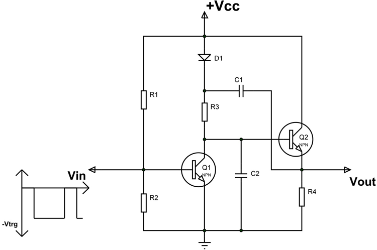
The circuit has main two components that are NPN transistors, namely Q1 and Q2. The transistor Q1 acts as a switch in this circuit and transistor Q2 is fitted to act as an emitter follower. The diode D1 is present here for preventing the discharge of capacitor C1 in the wrong way. The resistors R1 and R2 are present here for biasing the transistor Q1 and keeping it turned ON by default.
As mentioned above, the transistor Q2 acts in emitter follower configuration, so whatever the voltage appears at the base of the transistor, the same value will appear at its emitter. So the voltage at the output ‘Vo’ is equal to the voltage at the base of the transistor, which is the voltage across capacitor C2. The resistor R4 and R3 are present here to protect the transistors Q1 and Q2 from high currents.
From the start, the transistor Q1 is turned ON because of biasing and because of this, the capacitor C2 will be completely discharged through Q1 which in turn results in output voltage becoming zero. So when Q1 is not triggered, the output voltage Vo is equal to zero.
At the same time, when Q1 is not triggered, the capacitor C1 will be completely charged to voltage +Vcc through diode D1. During the same time, when Q1 is ON the base of Q2 will be driven to the ground to keep the transistor Q2 OFF state.
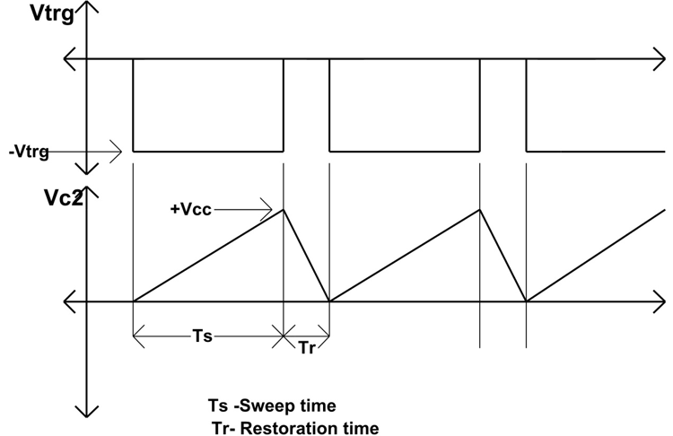
Since the transistor Q1 is ON by default, to turn it OFF a negative trigger of duration ‘Ts’ is given to the gate of transistor Q1 as shown in the graph. Once the transistor Q1 enters high impedance state, the capacitor C1 which is charged to voltage +Vcc will try to discharge itself.
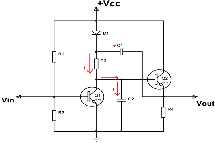
So a current ‘I’ flows through the resistor and to the capacitor C2 as shown in the figure. And because of this current flow, the capacitor C2 starts charging and a voltage ‘Vc2’ will appears across it.
In the bootstrap circuit, the capacitance of C1 is very much higher than C2, so the electric charge stored by capacitor C1 when it is fully charged is very high. Now even if the capacitor C1 is discharging itself, the voltage across its terminals will not change much. And because of this stable voltage across capacitor C1, the current ‘I’ value will be stable through the discharge of the capacitor C1.
With the current ‘I’ being stable throughout the process, the rate of charge received by the capacitor C2 will also be stable throughout. With this stable accumulation of charge, the capacitor C2 terminal voltage will also rise slowly and linearly.
Now with the capacitor C2 voltage is rising linearly with time, the output voltage also rises linearly with time. You can see in the graph during the trigger time ‘Ts’ the terminal voltage across capacitor C2 rising linearly with respect to time.
After the end of trigger time if the negative trigger given to transistor Q1 is removed, then the transistor Q1 will enter in the low impendence state by default and act as a short circuit. Once this happens, the capacitor C2 which is in parallel with transistor Q1 will discharge itself completely to have its terminal voltage drop sharply. So during the restoration time ‘Tr’ the terminal voltage of capacitor C2 will drop sharply to zero and the same could be seen in the graph.
Once this cycle of charge and discharge is completed, the second cycle will start with the gate trigger of transistor Q1. And because of this continuous triggering, a sawtooth waveform is formed at the output, which is the end result of the Bootstrap Sweep circuit.
Here the capacitor C2 which helps in providing constant current as feedback to the capacitor C1 is called ‘Bootstrapping capacitor’.

Excelente tutorial, muchas gracias por compartir sus conocimientos.