
Logic gates are the essential building blocks of digital circuits. These basic logic gates are used in Embedded Systems, Microcontrollers, Microprocessors, etc. Let us learn how to design the logic gates using VHDL in ModelSim. This tutorial is all about designing the basic logic gates using different VHDL modeling and their corresponding simulations. If you haven’t installed the ModelSim software, please refer to the previous tutorial “Getting Started with VLSI and VHDL using ModelSim -A Beginner's Guide” for installation guidance.
Creating a new Project in ModelSim
Before scripting the VHDL program, first, we need to create a project in the ModelSim. The steps to create the project are given below.
Step 1: Open ModelSim

Step 2: Click File---->New---->Project

Step 3: The create new project dialog box opens up. Enter the name for your project and click OK as shown below. For example, the project name given below is “basic_logicgates”

Step 4: The project will be created and the “Add Items to the project” dialog box opens. Click on Create New File.

Step 5: 'Create a new project file' opens up. Give a file name and choose the file type as VHDL and click OK. Here, for example, the file name is given as OR_gate.

Step 6: The project will be created and the file OR_gate will be added as shown below.

Step 7: Now that the file is added, we can start scripting our first VHDL program. Double click the OR_gate.vhd, an editor will open up on the right side of the window.

Let us start designing the basic logic gates using VHDL.
OR Gate
The Boolean function and Truth Table of the OR gate are given below. If you want to know the basics like what is or gate and how it works, you can check out the link for our previous tutorial.
OR Gate Symbol:

OR Gate Truth Table:
|
A |
B |
Y= A + B |
|
0 |
0 |
0 |
|
0 |
1 |
1 |
|
1 |
0 |
1 |
|
1 |
1 |
1 |
|
|
|
|
VHDL OR Gate:
Now that we know the Truth Table, let's start scripting the VHDL code for OR Gate. To understand the general structure of the VHDL code, please refer to the first tutorial.
Library IEEE;
use IEEE.std_logic_1164.all;
entity OR_gate is
    port(A : in std_logic;
         B : in std_logic;
         Y : out std_logic);
end OR_gate;
architecture orLogic of OR_gate is
 begin
    Y <= A OR B;
end orLogic;
First the Libraries are imported.
library IEEE;
use IEEE.std_logic_1164.all;
Next, the entity declaration is done by assigning the Input and Output Ports. Here, the entity name is declared as OR_gate.
Important Note: The Entity name should be the same as the file name as in Step 5. We named the file OR_gate therefore, the entity name should also be OR_gate.
Since A and B are the inputs, variables A and B are mapped to “in std_logic”. Here “in” refers to the input and std_logic refers to the standard signal/waveform. Similarly Y is mapped to “out std_logic” which refers to the output. Finally, the entity declaration is terminated by “end OR_gate”.
entity OR_gate is
    port(A: in std_logic;
         B: in std_logic;
         Y: out std_logic);
end OR_gate;
Once the entity is declared, the next step is to define the architecture of the entity (OR_gate). The architecture name is given as “orLogic”. The architecture of the entity (OR_gate) is defined by “architecture orLogic of OR_gate is”. Now that we know Y is the output, we know that output is nothing but the OR operation of the two inputs A and B. So, Y is mapped to A OR B (Y<=A OR B). The Boolean operator ‘OR’ is used to perform the OR operation between A and B. The architecture is terminated by “end orLogic”
architecture orLogic of OR_gate is
 begin
    Y <= A OR B;
end orLogic;
Now that you have completed scripting the VHDL code for OR Gate, let's compile and simulate the same.
How to Compile and Simulate Code on Modelsim?
Step 1: First save the File by Ctrl+S. On the Tool Bar of the ModelSim, there is an option called “Compile”. Click Compile>>>Compile All.

Step 2: Once Compiled All is clicked. The files are compiled and we can see a green tick mark “ü” and “Compile of entity name.vhd was successful” as shown below.

Step 3: If you find a red mark or unsuccessful please check your code if it has errors. Now that the compilation is successful. Let's simulate the designed circuit. On the ToolBar, there is an option called ”Simulate” as shown below. Click Simulate>>>Start Simulate.

Step 4: Once you select Start Simulation, a dialog box opens, and there is a folder called “Work”. Click Work Here, we can see our entity name (OR_gate). Select the “OR_gate” and click OK.

Step 5: The Simulation Window Opens. Right Click on the entity name (OR_gate) and click Add Wave as shown below.

Step 6: The waveform window opens with declared inputs and outputs on the right side of the window as shown below.

Step 7: Now, let us simulate the circuit by giving the inputs. Right Click on the Inputs A and B. A menu pops up from that choose “Force” option.


Step 8: Now a dialog box opens up. Set the Value to 0 for A and similarly for B set the value 0 and click OK.


Step 9: Now that the inputs are given, let's Run the simulation. There is a Run icon ![]() in the toolbar near the timer as shown below. Click the run icon, we can see the waveforms on the graph for 100 ps. There is a yellow colour cursor on the waveform, move the cursor so that the corresponding inputs and outputs are shown.
in the toolbar near the timer as shown below. Click the run icon, we can see the waveforms on the graph for 100 ps. There is a yellow colour cursor on the waveform, move the cursor so that the corresponding inputs and outputs are shown.

Now, we can see that for A=0, B=0, Y=0, which verifies with Truth Table of OR Gate. Similarly, the other four input combinations are given and their outputs are verified as shown below.

From the waveform graph, the output Y changes according to the given Inputs A and B. Now that all the input combinations for A and B (00,01,10,11) are forced to the input signals. Move the cursor throughout the waveform graph from 0ps to 500ps. The values of A, B, Y at corresponding time intervals are given below.
|
Timing(ps) |
A |
B |
Y |
|
0-100 |
0 |
0 |
0 |
|
100-200 |
0 |
1 |
1 |
|
200-300 |
1 |
0 |
0 |
|
300-400 |
1 |
0 |
0 |
|
400-500 |
1 |
1 |
1 |
The above values of A, B, Y corresponds to the Truth Table of the OR Gate.
This is how the VHDL logic gate codes are written, compiled, and simulated. Learners are encouraged to learn how to compile, force the input values, simulate as these steps won't be repeated in the forthcoming tutorials.
AND Gate
If you want to know the basics like what is AND gate and how it works, you can check out the link for our previous tutorial. The AND gate symbol and AND gate truth table are shown below.
AND Gate Symbol:

Truth Table for AND Gate:
|
A |
B |
Y=A.B |
|
0 |
0 |
0 |
|
0 |
1 |
0 |
|
1 |
0 |
0 |
|
1 |
1 |
1 |
VHDL Code for AND Gate:
library IEEE;
use IEEE.std_logic_1164.all;
entity andd_Gaate is
    port(A: in std_logic;
         B: in std_logic;
         Y: out std_logic);
end andd_Gaate;
architecture andLogic of andd_Gaate is
begin
    Y <= A AND B;
end andLogic;
First the libraries are imported.
library IEEE;
use IEEE.std_logic_1164.all;
The entity is decalred as andd_Gaate and A,B are decalred as inputs , Y is decalred as Output.
entity andd_Gaate is
    port(A: in std_logic;
         B: in std_logic;
         Y: out std_logic);
end and_gate;
Once the entity is declared, the next step is to define the architecture of the entity (andd_Gaate). The architecture name is given as “andLogic”. The architecture of the entity(and_gate) is defined by “architecture andLogic of andd_Gaate is”. Now that we know Y is the output, we know that output is nothing but the AND operation of the two inputs A and B. So, Y is mapped to A AND B(Y<=A AND B). The Boolean operator ‘AND’ is used to perform the AND operation between A and B. The architecture is terminated by “end andLogic”
architecture andLogic of andd_Gate is
begin
    Y <= A AND B;
end andLogic;
The above code is compiled, simulated with different input values as shown below.

Now that all the input combinations for A and B(00,01,10,11) are forced to the input signals, move the cursor throughout the waveform graph from 0ps to 400ps. The values of A,B,Y at corresponding time intervals are given below.
|
Timing(ps) |
A |
B |
Y |
|
0-100 |
0 |
0 |
0 |
|
100-200 |
0 |
1 |
0 |
|
200-300 |
1 |
0 |
0 |
|
300-400 |
1 |
1 |
1 |
The above values of A,B,Y corresponds to the Truth Table of the AND Gate.
NOT Gate
If you want to know the basics like what is NOT gate and how it works, you can check out the link for our previous tutorial. The NOT gate symbol and NOT gate truth table is shown below.
NOT Gate Symbol:

Truth Tabel for NOT Gate:
|
A |
Y=Ā |
|
0 |
1 |
|
1 |
0 |
VHDL Code for NOT Gate:
library IEEE;
use IEEE.std_logic_1164.all;
entity not_gate is
    port(A : in std_logic;
         Y : out std_logic);
end not_gate;
architecture notLogic of not_gate is
begin
    Y <= not(A) ;
end notLogic;
First, the libraries are imported.
library IEEE;
use IEEE.std_logic_1164.all;
The entity is declared as not_gate and A is declared as input, Y is declared as Output.
entity not_gate is
    port(A: in std_logic;
         Y: out std_logic);
end not_gate;
Once the entity is declared, the next step is to define the architecture of the entity (not_gate). The architecture name is given as “andLogic”. The architecture of the entity(not_gate) is defined by “architecture notLogic of not_gate is”. Now that we know Y is the output, we know that output is nothing but the NOT operation of the input A. So, Y is mapped to NOT(A) (Y<=NOT(A)). The Boolean operator ‘NOT’ is used to perform the NOT operation for A. The architecture is terminated by “end notLogic”
The code is compiled, and the input values are forced to simulate the NOT gate as shown below.
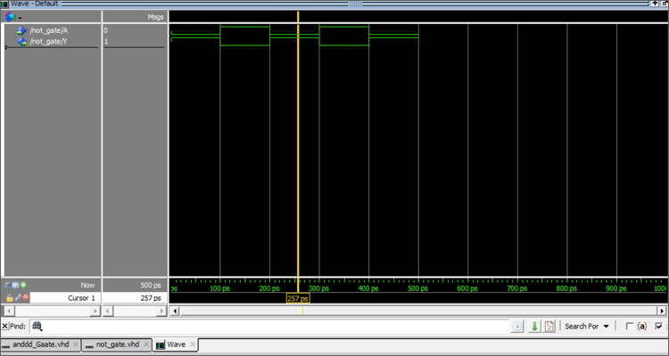
Now that all the input combinations for A (0,1) are forced to the input signals, move the cursor throughout the waveform graph from 0ps to 500ps. The values of A, B at corresponding time intervals are given below.
|
Timing(ps) |
A |
Y |
|
0-100 |
0 |
1 |
|
100-200 |
1 |
0 |
|
200-300 |
0 |
1 |
|
300-400 |
1 |
0 |
|
400-500 |
0 |
1 |
The above values of A,Y corresponds to the Truth Table of the NOT Gate.
NOR Gate
If you want to know the basics like what is NOR gate and how it works, you can check out the link for our previous tutorial. The NOR gate symbol and NOR gate truth table is shown below.
NOR Gate Symbol:

Truth Table for NOR Gate:
|
A |
B |
|
|
0 |
0 |
1 |
|
0 |
1 |
0 |
|
1 |
0 |
0 |
|
1 |
1 |
0 |

VHDL Code for NOR Gate: Since, the NOR gate is the complement of the OR Gate, the outputs of the OR gates are inverted. The VHDL code is given below.
library IEEE;
use IEEE.std_logic_1164.all;
entity nor_gate is
    port(A: in std_logic;
         B: in std_logic;
         Y: out std_logic);
end nor_gate;
architecture norLogic of nor_gate is
 begin
    Y <= not(A OR B);
end norLogic;
First, the libraries are imported.
library IEEE;
use IEEE.std_logic_1164.all;
The entity is declared as nor_gate and A, B are declared as inputs, Y is declared as Output.
entity nor_gate is
    port(A: in std_logic;
         B: in std_logic;
         Y: out std_logic);
end nor_gate;
Once the entity is declared, the next step is to define the architecture of the entity (nor_gate). The architecture name is given as “norLogic”. The architecture of the entity(nor_gate) is defined by “architecture norLogic of nor_gate is”. Now that we know Y is the output, we know that output is nothing but the complement of OR operation of the two inputs A and B. So Y is mapped to NOT(A OR B) (Y<=NOT (A AND B)). The Boolean operator ‘OR’ is used to perform the OR operation between A and B. For complementing the OR operation NOT operator is used. The architecture is terminated by “end norLogic”
The above code is compiled, simulated with different input values as shown below.

NAND Gate
If you want to know the basics like what is NAND gate and how it works, you can check out the link for our previous tutorial. The NAND gate symbol and NAND gate truth table is shown below.
NAND Gate Symbol:

Truth Table for NAND Gate:
|
A |
B |
|
|
0 |
0 |
1 |
|
0 |
1 |
1 |
|
1 |
0 |
1 |
|
1 |
1 |
0 |

VHDL Code for NAND Gate:
The output of the NAND Gate is nothing but the compelemnt of the AND Gate.
 library IEEE;
use IEEE.std_logic_1164.all;
entity nand_gate is
    port(A: in std_logic;
         B: in std_logic;
         Y: out std_logic);
end nand_gate;
architecture nandLogic of nand_gate is
begin
    Y <= not (A and B);
end nandLogic;
First, the libraries are imported.
library IEEE;
use IEEE.std_logic_1164.all;
The entity is declared as nand_gate and A,B are declared as input, Y is declared as Output.
entity nand_gate is
    port(A: in std_logic;
         B: in std_logic;
         Y: out std_logic);
end nand_gate;
Once the entity is declared, the next step is to define the architecture of the entity (nand_gate). The architecture name is given as “nandLogic”. The architecture of the entity(nand_gate) is defined by “architecture nandLogic of nand_gate is”. Now that we know Y is the output, we know that output is nothing but the complement of AND operation of the two inputs A and B. So, Y is mapped to NOT(A AND B) (Y<=NOT (A AND B)). The Boolean operator ‘AND’ is used to perform the AND operation between A and B. For complementing the AND operation NOT operator is used. The architecture is terminated by “end nandLogic”.
 architecture nandLogic of nand_gate is
begin
    Y <= not (A and B);
end nandLogic;
The above code is compiled, simulated with different input values as shown below.

Now that all the input combinations for A and B(00,01,10,11) are forced to the input signals, move the cursor throughout the waveform graph from 0ps to 400ps. The values of A, B, Y at corresponding time intervals is given below.
|
Timing(ps) |
A |
B |
Y |
|
0-100 |
0 |
0 |
1 |
|
100-200 |
0 |
1 |
1 |
|
200-300 |
1 |
0 |
1 |
|
300-400 |
1 |
1 |
0 |
The above values of A, B, Y corresponds to the Truth Table of the NAND Gate.
XOR Gate
If you want to know the basics like what is XOR gate and how it works, you can check out the link for our previous tutorial. The XOR gate symbol and XOR gate truth table is shown below.
XOR Gate Symbol:

Truth Table for XOR:
|
A |
B |
|
|
0 |
0 |
0 |
|
0 |
1 |
1 |
|
1 |
0 |
1 |
|
1 |
1 |
0 |

VHDL Code for XOR:
library IEEE;
use IEEE.std_logic_1164.all;
entity xor_gate is
    port(A: in std_logic;
         B: in std_logic;
         Y: out std_logic);
end xor_gate;
architecture xorLogic of xor_gate is
 begin
    Y <= A xor B;
end xorLogic;
First, the libraries are imported.
library IEEE;
use IEEE.std_logic_1164.all;
The entity is declared as xor_gate and A,B are declared as input, Y is declared as Output.
entity xor_gate is
    port(A: in std_logic;
         B: in std_logic;
         Y: out std_logic);
end xor_gate;
Once the entity is declared, the next step is to define the architecture of the entity (xor_gate). The architecture name is given as “xorLogic”. The architecture of the entity(xor_gate) is defined by “architecture xorLogic of xor_gate is”. Now that we know Y is the output, we know that output is nothing but the XOR operation of the two inputs A and B. So, Y is mapped to A XOR B(Y<=A XOR B). The Boolean operator ‘XOR’ is used to perform the OR operation between A and B. The architecture is terminated by “end xorLogic”
architecture xorLogic of xor_gate is
begin
    Y <= A XOR B;
end xorLogic;
The above code is compiled and simulated with different input values as shown below.

Now that all the input combinations for A and B(00,01,10,11) are forced to the input signals, move the cursor throughout the waveform graph from 0ps to 400ps. The values of A, B, Y at corresponding time intervals are given below.
|
Timing(ps) |
A |
B |
Y |
|
0-100 |
0 |
0 |
0 |
|
100-200 |
0 |
1 |
1 |
|
200-300 |
1 |
0 |
1 |
|
300-400 |
1 |
1 |
0 |
The above values of A, B, Y corresponds to the Truth Table of the XOR Gate.
XNOR Gate
If you want to know the basics like what is XNOR gate and how it works, you can check out the link for our previous tutorial. The XNOR gate symbol and XNOR gate truth table is shown below.
XNOR Gate Symbol:

Truth Table for XNOR Gate:
|
A |
B |
|
|
0 |
0 |
1 |
|
0 |
1 |
0 |
|
1 |
0 |
0 |
|
1 |
1 |
1 |

VHDL Code for XNOR Gate:
The output of the XNOR Gate is nothing but the complement of the XOR Gate.
library IEEE;
use IEEE.std_logic_1164.all;
entity xnor_gate is
    port(A : in std_logic;
         B : in std_logic;
         Y : out std_logic);
end xnor_gate;
architecture xnorLogic of xnor_gate i
 begin
    Y <= not(A xor B);
end xnorLogic;
First, the libraries are imported.
library IEEE;
use IEEE.std_logic_1164.all;
The entity is declared as xnor_gate and A,B are declared as inputs , Y is declared as Output.
entity xnor_gate is
    port(A: in std_logic;
         B: in std_logic;
         Y: out std_logic);
end xnor_gate;
Once the entity is declared, the next step is to define the architecture of the entity (xnor_gate). The architecture name is given as “xnorLogic”. The architecture of the entity(xnor_gate) is defined by “architecture xnorLogic of xnor_gate is”. Now that we know Y is the output, we know that output is nothing but the complement of the XOR operation of the two inputs A and B. So Y is mapped to NOT(A XOR B) (Y<=NOT (A XOR B)). The Boolean operator ‘XOR’ is used to perform the AND operation between A and B. For complementing the XOR operation NOT operator is used. The architecture is terminated by “end xorLogic”.
architecture xnorLogic of xnor_gate i
 begin
    Y <= not(A xor B);
end xnorLogic;
The above code is compiled and simulated with different input values as shown below.

Now that all the input combinations for A and B(00,01,10,11) are forced to the input signals, move the cursor throughout the waveform graph from 0ps to 400ps. The values of A, B, Y at corresponding time intervals are given below.
|
Timing(ps) |
A |
B |
Y |
|
0-100 |
0 |
0 |
1 |
|
100-200 |
0 |
1 |
0 |
|
200-300 |
1 |
0 |
0 |
|
300-400 |
1 |
0 |
1 |
The above values of A, B, Y corresponds to the Truth Table of the XNOR Gate.
Complete Project Code
Library IEEE;

use IEEE.std_logic_1164.all;

entity OR_gate is

    port(A : in std_logic;

         B : in std_logic;

         Y : out std_logic);

end OR_gate;

architecture orLogic of OR_gate is

 begin

    Y <= A OR B;

end orLogic;

use IEEE.std_logic_1164.all;

entity andd_Gaate is

    port(A : in std_logic;

         B : in std_logic;

         Y : out std_logic);

end andd_Gaate;

architecture andLogic of andd_Gaate is

begin

    Y <= A AND B;

end andLogic;

library IEEE;

use IEEE.std_logic_1164.all;

entity not_gate is

    port(A : in std_logic;

         Y : out std_logic);

end not_gate;

architecture notLogic of not_gate is

begin

    Y <= not(A) ;

end notLogic;

library IEEE;

use IEEE.std_logic_1164.all;

entity nor_gate is

    port(A : in std_logic;

         B : in std_logic;

         Y : out std_logic);

end nor_gate;

architecture norLogic of nor_gate is

 begin

    Y <= not(A OR B);

end norLogic;

The output of the NAND Gate is nothing but the compelemnt of the AND Gate.

 library IEEE;

use IEEE.std_logic_1164.all;

entity nand_gate is

    port(A : in std_logic;

         B : in std_logic;

         Y : out std_logic);

end nand_gate;

architecture nandLogic of nand_gate is

begin

    Y <= not (A and B);

end nandLogic;

library IEEE;

use IEEE.std_logic_1164.all;

entity xor_gate is

    port(A : in std_logic;

         B : in std_logic;

         Y : out std_logic);

end xor_gate;

architecture xorLogic of xor_gate is

 begin

    Y <= A xor B;

end xorLogic;

library IEEE;

use IEEE.std_logic_1164.all;

entity xnor_gate is

    port(A : in std_logic;

         B : in std_logic;

         Y : out std_logic);

end xnor_gate;

architecture xnorLogic of xnor_gate i

 begin

    Y <= not(A xor B);

end xnorLogic;
