

Snubbers are the energy absorbing circuits used to smooth the voltage spikes caused due to the circuit’s inductance. Sometimes, due to the overcurrent, overvoltage and overheating the component gets fail. So, for the overcurrent protection of the circuit we use fuses at suitable locations and for overheating we use heat sinks or fans.
Snubber circuits are used for limiting the rate of change in voltage or current (di/dt or dv/dt) and overvoltage during turning ON and OFF the circuit. A Snubber circuit is the combination of resistors and capacitors connected in series across the switch like transistor or Thyristor for the protection as well as for improving performance. Snubber circuits are also used across the switches and relays to prevent arcing.
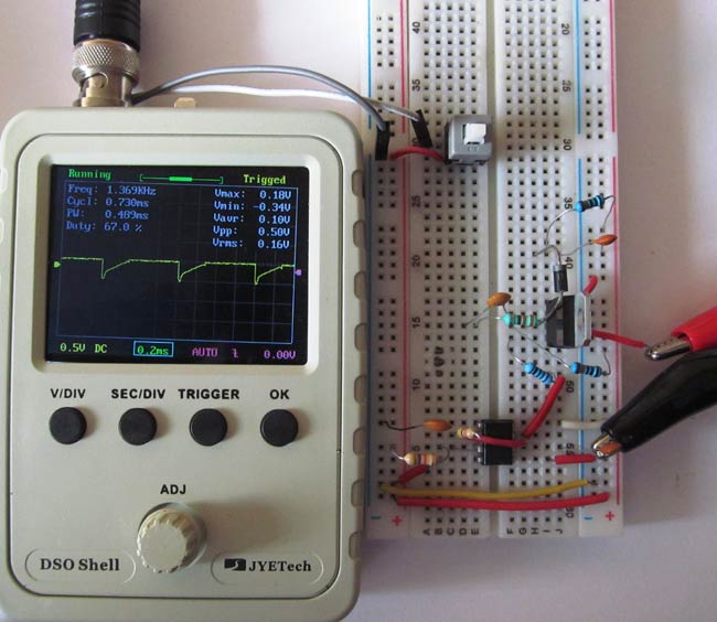
In this project, we will show you how a Snubber circuit protects a Thyristor from overvoltage or overcurrent. The circuit is consisting of Snubber circuit across the Thyristor and a frequency generator circuit using 555 timer IC.
Material Required
- Thyristor-TYN612 (SCR)
- 555 timer IC
- Resistor (47k-2,10k-2,1k-1,150-1)
- Capacitor (0.01uf,0.001uf,0.1uf-2)
- Diode-1N4007
- Switch
- Oscilloscope (for output confirmation)
- 9v supply
- Connecting wires
Circuit Diagram

Thyristor - TYN612
Here, in the name of Thyristor TYN612, ‘6’ indicates the value of Repetitive peak off-state voltage, VDRM and VRRM is 600 V and ‘12’ indicates the value of On-state RMS current, IT (RMS) is 12 A. Thyristor TYN612 is fit for all modes of control like overvoltage crowbar protection, motor control circuit, inrush current limiting circuits, capacitive discharge ignition and voltage regulation circuits. The range of triggering gate current (IGT) is 5 mA to 15 mA. The operating temperature ranges from -40 to 125 °C. Learn more about the Thyristor here.
Pinout Diagram of Thyristor TYN612
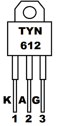
Pin Configuration of Thyristor TYN612
|
Pin NO. |
Pin Name |
Description |
|
1 |
K |
Cathode of Thyristor |
|
2 |
A |
Anode of Thyristor |
|
3 |
G |
Gate of Thyristor, used for triggering |
Design of Snubber Circuit
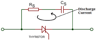
As we know, a Snubber circuit is the combination of resistor and capacitor. Capacitor, used in Snubber circuit, is able to prevent the device from unwanted dv/dt triggering of the Thyristor or SCR. As the voltage is applied to the circuit a sudden voltage appears across the switching device. The capacitor Cs behaves like a short circuit which results in zero voltage across the SCR. As the time flies, the voltage across the capacitor Cs builds up at a slow rate. So, the value of dv/dt across the capacitor C2 and Thyristor gets decrease than the maximum dv/dt rating of the device.
Now, the question is what is the use of resistance RS? When the SCR is turned ON, capacitor discharges through the SCR and sends a current equal to Vs/RS. As the resistance is quite LOW, the di/dt will tend to be high enough that may damage the SCR. So, in order to limit the magnitude of discharge current resistance RS is used.
Working of Snubber Circuit
The circuit is divided into two parts. The first one is used as a frequency generator circuit using a 555 timer IC whose output is used to feed the gate terminal of Thyristor. The second part of the circuit is used to check the switching of the Thyristor or SCR with the Snubber circuit and without the Snubber circuit.
Case I: Without Snubber Circuit

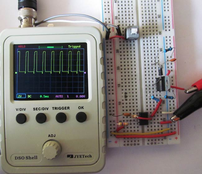
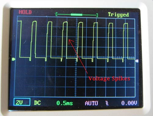
When the Snubber circuit is not present across the SCR as shown in the circuit above, high voltage spikes occur as you can see in the waveform below. So for smoothing the voltage spikes, we use a Snubber circuit which prevents the device to get damaged due to overvoltage or dv/dt false triggering.
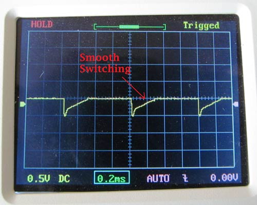
Case II: With Snubber Circuit
When Snubber circuit is present across the SCR, it reduces or smoothes the voltage spikes as shown in the waveform below. Therefore, the device will not get damaged due to overvoltage and it also reduces the dv/dt value of the device than the maximum rating.

Hi Did you use the SCR at 100Khz frequency? because generally you can use SCR for upto couple of hundred Hz??