

In the field of DC-DC Converters, A single-ended primary-inductor converter or SEPIC converter is a type of converter that uses a boost type control topology to step up or step down the input voltage. After reading this, the first question that will come to your mind would be, is it like a glorified Classic Buck-Boost Converter? The answer is yes and no. A classic buck-boost converter consists of two inductors and two switches that increase the cost, so to reduce it, a much more complex topology known as the inverting buck-boost converter is used. We have discussed it in one of our previous articles. In an Inverting buck-boost converter, the output polarity of the inverting buck-boost converter is opposite to that of the input. A sepic converter addresses these issues by introducing a coupled inductor that reduces the overall cost and also takes less space in the actual circuit board.
So in this article, we are going to learn how to build, and test a simplified Sepic converter built on top of the popular XL6009 IC. We have previously used this XL6009 IC to Design a Mobile Power bank and an Adjustable Buck-Boost Regulator (3.3V to 12V), you can also check them out if you are interested.
Working of SEPIC Converter (Single-Ended Primary-Inductor Converter)
The schematic below is a basic schematic of a SEPIC converter and in this article, we are going to use this to explain the working principle.
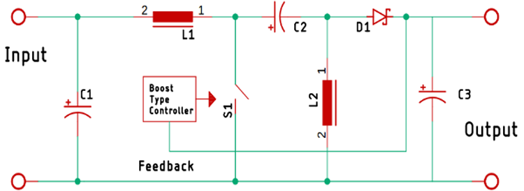
SEPIC converter is a buck-boost topology, unlike the classic buck-boost that is an inverting topology. A SEPIC converter is characterized by using two inductors, one is at the input and another one is connected to the ground and these two inductors are connected by a coupling capacitor, which effectively puts the L1 and L2 in parallel when a switching signal is applied.
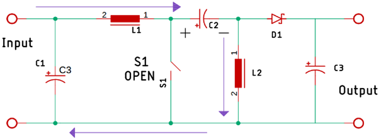
Now, to understand the working of the SEPIC converter we have modified the basic circuit and removed the controller from the picture. As you can see when the power is applied to the circuit at that brief moment the switch is open and the capacitor C2 starts charging through the inductor L1. Now as the controller IC turns on, it turns on the switch.
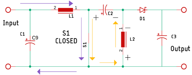
Now, as the switch is turned on, two things happen simultaneously, first the inductor L1 and L2 start charging simultaneously. When that happens, the switch gets opened because of the PWM pulse that is generated by the internal circuit of the XL6009 IC.
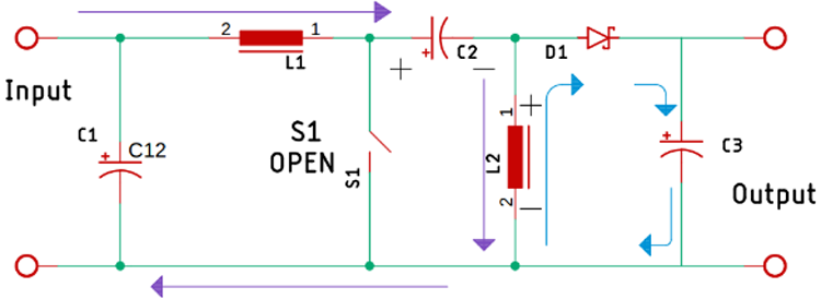
Now, as the switch is turned off again, the inductor changes its polarity and discharges through the diode, and at this moment, the output capacitor C3 holds the charges. And depending on the PWM signal and feedback, now we can change the output voltage in a very stable manner. This was a very basic explanation of how a SEPIC converter works.
At this moment, if you are wondering what is the use of the L1 in this schematic then? Now, look at the schematic very carefully: The inductor you see on the circuit diagram is a coupled inductor that means two windings are connected in a single core. It’s done to reduce transients. So, one of the issues in designing with separate inductors are the two inductors, L1 and L2 with the capacitor in series form a resonance circuit, and as we all know from the circuit theory, for a step response in an LC circuit, the input voltage can rise twice the input voltage so it may damage your sensitive lab power supply. So, the way to minimize the issue is to use a SEPIC with a coupled inductor. When we do that, the energy gets coupled by the SEPIC coupling capacitor. Without the coupling capacitor, this circuit will work as a flyback converter. The coupling capacitor shorts any leakage voltage and allows the circuit to work more efficiently. In these types of coupled inductor converters, the two inductors should have the same value that is why we need to build our inductor.
Components Required to Build SEPIC Converter
Components required for building the XL6009 Boost Converter IC Based SEPIC Buck-Boost Converter are listed below. The components used in this project are very generic and you can find most of them in your local hobby store.
- XL6009 IC - 1
- 470uF,63V capacitor - 1
- 220uF,63V capacitor - 1
- 22uF,63V capacitor - 1
- 1uF,50V SMD 0805 Capacitor - 2
- MBR20100CT Diode - 1
- 10K Resistor - 1
- 10K Potentiometer - 1
- Screw Terminal - 2
- 47uH Coupled Inductor - 1
- Jumper Wires - 1
- Cladboard - 1
Schematic Diagram for XL6009 Based SEPIC Converter
The Complete Schematic diagram for the XL6009 based SEPIC converter is shown below.

The working principle of this circuit is very simple. First, we have our input storage capacitor that is directly connected to the input VCC pin of the IC. Next, we have our coupling capacitor, a 47uH 4A coupled inductor is recommended on the example schematic that is taken from Fig 6 of the Xl6009 datasheet. The coupled inductor can be any type; it can be a coupled transformer or in my case, it is a toroidal bobbin that we have disordered out from an old non-working ATX power supply. The output diode is a MUR810 diode that is 8A and 100V. Next, we have our feedback circuit that consists of a 10K resistor and a 10K potentiometer. Finally, we have our output capacitors that store the output voltage. Once we are done with the soldering process, the board looks like the image shown below.

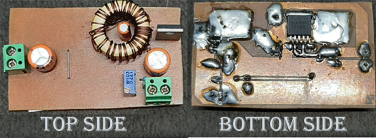
PCB for XL6009 Based SEPIC Converter
The PCB for our SEPIC Buck-Boost Converter circuit is designed on a single-sided board. I have used Eagle to design my PCB but you can use any PCB design software of your choice. The 2D image of the top and bottom of the PCB that is generated by Eagle is shown below.

As you can see on the very left of the PCB, we have our Input power connector and on the bottom right corner, we have our output connector. We have used a capacitor in the middle of the coupled inductor as it was very convenient to put it there, the capacitor C3 on the PCB is the capacitor C2 that we have shown in our basic schematic. The main driver of this SEPIC converter is the XL6009 IC, it’s on the bottom of the PCB . As it’s an SMD component, we had to place it on the bottom. We have used a thick ground plane to ensure sufficient current can flow through it. The complete design file along with TL494 Boost converter schematics can be downloaded from the link below.
Handmade PCB:
For convenience, I prepared my handmade version of the PCB and it's shown below. I made some mistakes while making this PCB, so I had to use some copper wires as jumpers to fix that.
Testing the XL6009 Based SEPIC Buck-Boost Converter Circuit
Note: While powering this circuit for the first time, do use a Constant Current Power Supply to limit the current or you can use a bunch of power resistors to limit the current. If you have made some mistakes while the soldering process, the XL6009 may burn out.

As you can see, the above test setup is used to test the circuit. An ATX PC, power supply is used to power the circuit which is why the input voltage stays at 12V. You can also see that the circuit is currently operating in boost mode so the output stays at 43.26V volts in this condition and I have attached a minimal load of 2.2K 1W resistor to the circuit and it was drawing around .02A of current.

The image above shows that this circuit can reach a minimum voltage of 2.5V at minimum load conditions.
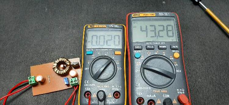
Since I only have two multimeters at my disposal, I have used the mecho 450B+ Multimeter to display the output voltage and I have used the MECHO 108B+ Multimeter to measure the output current.
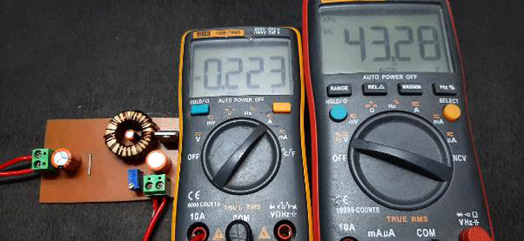
In the above picture, the output voltage from the SEPIC converter stays the same as 43.28V which means the output current also stays the same. But in the MECHO 108B+ Multimeter, you can see that the current has risen to .223A or 223 mA. It is because in the above picture, the MECHO 108B+ Multimeter is showing the input current and as I am powering the circuit with an ATX power supply, the input voltage stays at 12V.
Now, for the efficiency in the lower voltage range, I was able to get an efficiency of about 68% but at the higher voltage range, the efficiency got down at about 40%. This happens only because of the poor-quality inductor. So, the quality of the inductor must be very good. An EE core will do a much better job than a toroidal core.
Further Enhancements
This SEPIC buck-boost converter circuit is for demonstration purposes only, hence, no protection circuit is added in the output section of the circuit.
- An output protection circuit must be added to protect the load circuit.
- The inductor needs to be dipped into varnish otherwise it will generate audible noise.
- A good quality PCB with a proper design is mandatory
- The switching transistor can be modified to increase the load current.
- The quality of the inductor must be very good.
- To get maximum efficiency out of the circuit, the inductor should be able to handle a maximum current of 4A as defined on the XL6009 datasheet.
I hope you liked this article and learned something new out of it. If you have any doubt, you can ask in the comments below or can use our forums for detailed discussion.
