

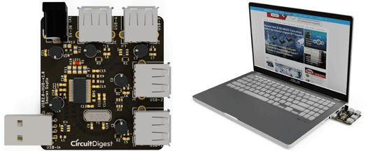
Today, our desks are full of devices that require connection to be connected with the PC via USB, or we need to work with multiple devices that have USB ports. It became a problem as Laptops lack multiple ports, and this is where a USB hub or USB Port Extender comes in handy. This comprehensive guide demonstrates how to build a professional DIY USB hub with a power supply using the GL850G USB 2.0 hub IC, complete with overcurrent protection and self-powered capabilities.
A USB hub circuit board is a useful device that provides the flexibility to turn a single Universal Serial Bus (USB) port into a multi-port system, so we can connect more devices to a host system. In a multi-port USB HUB system, we can use multiple USB devices such as a mouse, keyboard, pen drives, and others, and the bandwidth of the host USB is shared among them. This project provides a detailed USB hub circuit diagram and USB hub schematic to help you create a 4-port DIY powered USB hub with professional-grade protection circuits and PCB design best practices.
The USB hub PCB boards built in this project were fabricated by our long-time sponsor, pcbway.com. For those who are new, PCBWay is a Fabrication and Assembly service provider that can provide high-quality, full-featured custom PCBs for prototype and manufacturing quantities. We will discuss more on how to use their services later, but if you want to get your hands on these USB hubs PCB boards, you can also check out the Project Giveaway, which is explained in the video linked at the bottom of this page.
Table of Contents
Why Build a DIY USB Hub?
- Cost-Effective: Build a custom 4-port hub for under $20 in components
- Learning Experience: Understand the USB 2.0 protocol and differential pair routing
- Customisation: Add features like individual port power control and external power options
- Professional Quality: Implement ESD protection and overcurrent safeguards
USB Hub Technical Specifications
- USB2.0 Facility
- 4 Dedicated Port.
- Self Power and External Power Option
The USB hub circuit will support the USB 2.0 facility and will have 4 Dedicated USB Ports. It can be self-powered, meaning it will take power from the Host USB Port and distribute it to other connected USB devices, or an external 5V power source will allow it to power the external devices.
Components Required for Building a DIY USB Hub Circuit Board
The following bill of materials (BOM) includes all components needed to assemble your DIY powered USB hub.
| Qty | Value | Package | Parts |
| 12 | 0.1uF | C0603 | C5, C6, C7, C8, C11, C12, C13, C15, C17, C18, C20, C21 |
| 1 | 100k | R0805 | R11 |
| 5 | 100uF | E2-5 | C1, C2, C3, C4, C22 |
| 1 | 10k | R0603 | R8 |
| 1 | 10k | R0805 | R6 |
| 1 | 10uF | E2-5 | C19 |
| 1 | 12MHz | XTAL_ECS-120-18-4X-CKM | Y1 |
| 2 | 1uF | C0603 | C14, C16 |
| 1 | 2.5A/30V/105mΩ | SOT23-3 | Q1 |
| 1 | 20k | R0805 | R7 |
| 2 | 33pF | C0603 | C9, C10 |
| 1 | 4.7k | R0805 | R12 |
| 1 | 470R | R0805 | R10 |
| 1 | 470k | R0805 | R13 |
| 1 | 47k | R0603 | R9 |
| 4 | 500mA | THRMC2012X50N | R1, R2, R3, R4 |
| 1 | 680R | R0603 | R5 |
| 1 | DC-Socket | DCJACK_2MM_PTH | CN1 |
| 6 | FB-0603-2A | INDC1608X95N | L1, L2, L3, L4, L5, L6 |
| 1 | GL850G-HH | SOP65P780X200-2N | IC1 |
| 1 | RED | CHIPLED_0805 | LED1 |
| 3 | SRV05-4 - ESD Protection | SOT95P280X145-6N | IC2, IC3, IC4 |
| 4 | USB-A-S-X-X-TH | SAMTEC_USB-A-S-X-X-TH | J1, J2, J3, J4 |
| 1 | USB-AM-S-X-X-TH | SAMTEC_USB-AM-S-X-X-TH | J5 |
The Bill of Materials has the component designator on the PCB. For the Schematic and the PCB, let's move to the next section -
Understanding the USB Hub Circuit Diagram
The complete USB hub schematic consists of several functional blocks working together to provide reliable USB port expansion. This section breaks down each circuit section to help you understand the design principles behind professional USB hub circuit boards. The complete schematic for the DIY USB Hub is given below:

Let's see how the components are connected. For better understanding, each section of the schematic is separated as a block, as per the working principle of each major component.
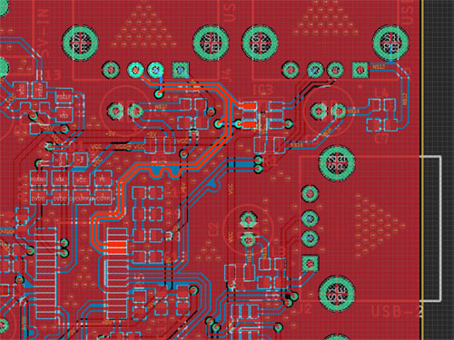
GL850G USB 2.0 Hub IC - The Heart of the Circuit
The Genesys Logic GL850G serves as the main USB 2.0 hub IC in this design. It is from Genesys Logic’s advanced version of Hub solutions, which fully comply with Universal Serial Bus Specification Revision 2.0.
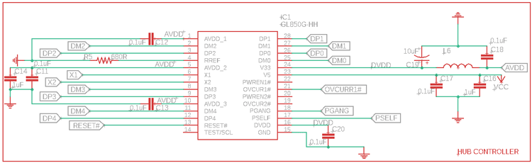
We have chosen this as it provides major advantages during the design process of the USB HUB.
It has both 5V to 3.3V and 3.3V to 1.8V voltage drop regulators in a single chip; therefore, external LDOs are not required, and the cost can be saved.
As a brief description, GL850G uses an 8-bit RISC processor to manipulate the control/status registers and respond to the requests from the USB host. GL850G also has pre-installed firmware that will control its general-purpose I/O and also access the external EEPROM.
In the above schematic, we are using the 4 downstream ports connected as DP1, DM1, DP2, DM2, and so on, up to DP4, DM4. This is the main USB D+ and D- connection that goes to the respective USB devices.
It is taking power through pin 25, which is a 5V line, and pin 24, which is a 3.3V pin. The 3.3V section has a PI filter, 0.1uF and 10uF capacitors and a ferrite bead to provide a clean supply as an analog voltage.
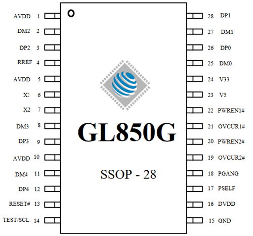
The pinout can be seen in the below-
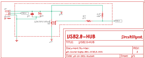
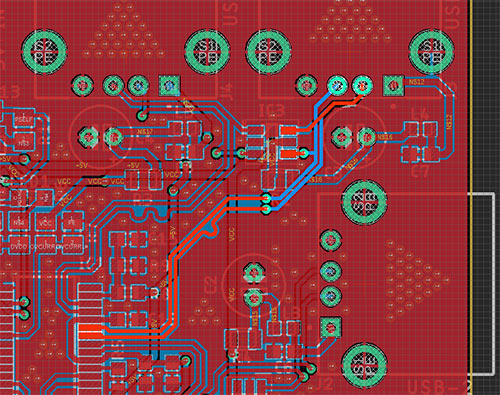
USB Host Connection and Overcurrent Protection Circuit
This is the Input of the USB. It has a male USB socket that will be inserted into the PC, Laptop, or device that has the USB HUB Feature. There is also an ESD protection being used, having the IC4, which will protect this upstream port from ESD. The upstream port section handles the connection between your DIY USB hub and the host computer. This circuit includes several protection mechanisms:
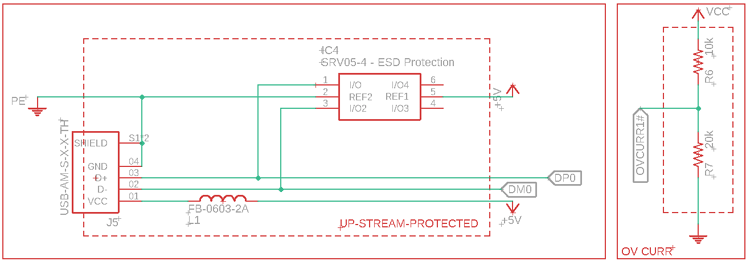
The overcurrent voltage divider is used to bias the overcurrent pin. The voltage divider is set to provide 3.3V at this pin to activate the overcurrent protection feature for the USB BUS on 4 ports.
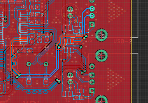
4-Port Downstream USB Hub Circuit Design
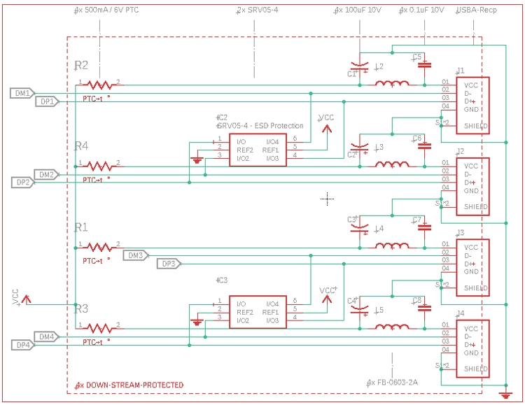
In the above image, 4 downstream ports are shown. All are using individual filters in the power line to provide clean power to the USB devices. However, there are 4 PTC available for protecting high current drives.
Each of the four downstream ports in this USB hub circuit diagram features individual protection and filtering components:
| Component | Function in USB Hub Circuit |
| PTC Fuses (F1-F4) | Resettable polyfuses protect against short circuits and overcurrent. When current exceeds 500mA, the PTC heats up and increases resistance, limiting current flow. Automatically resets when fault is cleared. |
| TVS Diodes (IC2, IC3) | Transient Voltage Suppression diodes clamp voltage spikes on D+ and D- lines, protecting downstream devices from ESD damage during hot-plugging events. |
| LC Filters | Inductor-capacitor filters on the power rail reduce switching noise and ensure clean 5V supply to connected USB devices. Critical for noise-sensitive peripherals. |
| 100µF Capacitors | Bulk capacitance provides current reserves during device enumeration and handles transient current demands when peripherals are first connected. |
| 0.1µF Bypass Caps | High-frequency ceramic capacitors filter switching noise and provide local charge storage for fast digital transitions. |
Other than that, IC2 and IC3 are the TVS diodes to protect the internal devices from the ESD surges.
Peripheral Support Circuits
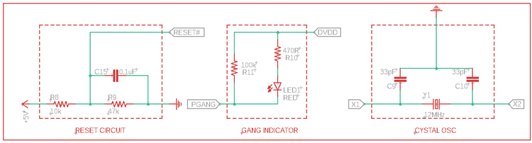
The first one is the Reset Circuit. This is a simple voltage divider for reset, which has a voltage output of 4V. So, when the 5V goes low, it could change the threshold voltage of the GL850G reset.
The middle one is the GANG indicator. When 4 USBs are active, this Indicator will be turned on.
The last one is the 12MHz crystal oscillator, used by the GL850G.
External Power Supply Logic and MOSFET Switching
In the above circuit, a MOSFET is controlled using the Battery connector Logic. At normal conditions, the MOSFET gets turned off, but when someone inserts a connector, the DC barrel connector switch gets disconnected and the power of 5V gets connected to the supply rail via the MOSFET. This DIY USB hub with power supply includes intelligent power source selection.
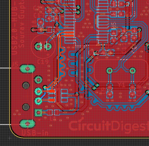
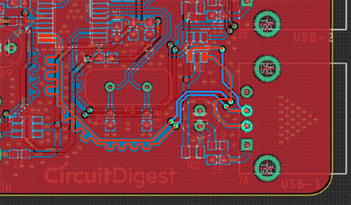
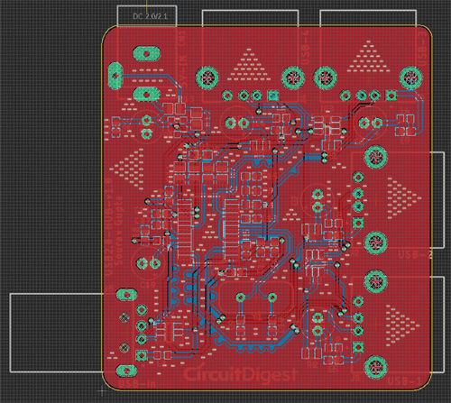
PCB Design for DIY USB Hub - Critical Layout Considerations
Proper PCB layout is crucial for a functional USB hub circuit board. Important traces are shown below where the USB differential pair lengths are matched. If you are new to differential routing in PCB design, you can check this article, which explains the importance of differential pair routing and how to use it.
| Design Parameter | Specification & Implementation |
| Differential Impedance | 90Ω ±10% (achieved with 0.2mm traces, 0.15mm spacing on FR4) |
| Length Matching | ±2mm maximum mismatch between D+ and D- within each pair |
| Trace Width | 0.2mm (8 mil) for 90Ω impedance on standard 1.6mm FR4 |
| Trace Spacing | D+ and D- spaced 0.15mm apart, minimum 0.5mm to other signals |
| Via Usage | Minimize vias in differential pairs; if required, use vias on both traces |
| Ground Plane | Continuous ground plane beneath differential pairs for reference |
The section below is the Input USB.
This is the USB 1 trace.
This is the USB 2 trace.
This is the USB 3 trace.
This is the USB 4 trace.
This is the Whole PCB
3D PCB Visualisation
The PCB is converted to 3D before making the design -
Before ordering, visualise your USB hub circuit board in 3D to verify component placement, connector alignment, and mechanical fit:
Ordering Your USB Hub PCB from PCBWay
Before ordering, visualise your USB hub circuit board in 3D to verify component placement, connector alignment, and mechanical fit. PCBWay offers professional PCB fabrication services ideal for DIY USB hub projects.
Now, after finalising the design, you can proceed with ordering the PCB:
⇒ Step 1: Go to https://www.pcbway.com/, sign up if this is your first time. Then, in the PCB Prototype tab, enter the dimensions of your PCB, the number of layers, and the number of PCBs you require.
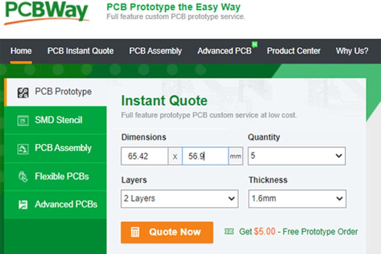
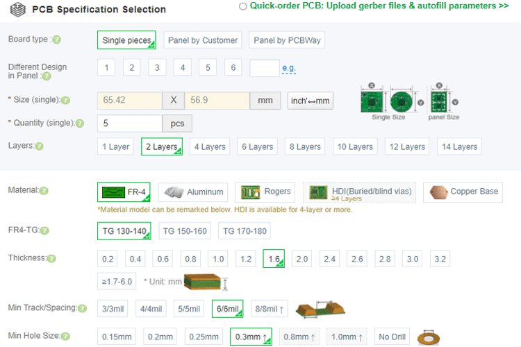
⇒ Step 2: Proceed by clicking on the ‘Quote Now’ button. You will be taken to a page where to can set a few additional parameters like the Board type, Layers, Material for PCB, Thickness, and More. Most of them are selected by default; if you are opting for any specific parameters, you can select them here.
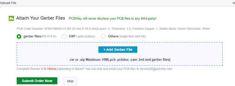
⇒ Step 3: The final step is to upload the Gerber file and proceed with the payment. To make sure the process is smooth, PCBWAY verifies if your Gerber file is valid before proceeding with the payment. This way, you can be sure that your PCB is fabrication-friendly and will reach you as committed.
Assembling Your DIY USB Hub Circuit Board
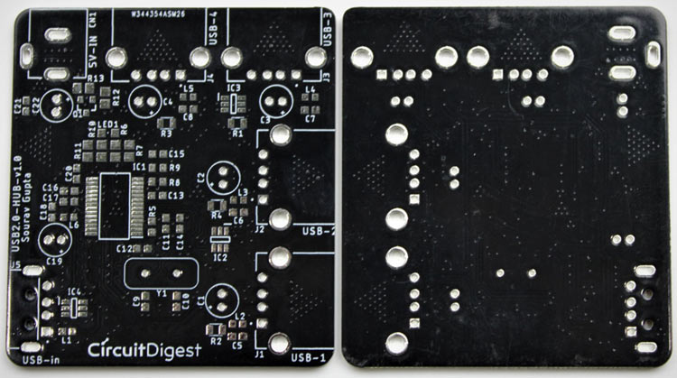
After the board was ordered, it reached me after some days through courier in a neatly labelled, well-packed box. The PCB quality was good as always. The top layer and the bottom layer of the board are shown below:
Once your USB hub PCB arrives, follow this systematic assembly process:
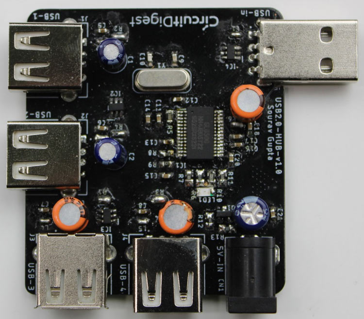
After making sure the tracks and footprints were correct. I proceeded with the assembly of the PCB. The completely soldered board looks like the one below:
3D Printing a Custom Enclosure for Your USB Port Extender
A professional enclosure protects your DIY powered USB hub from physical damage and provides a clean, finished appearance. After assembling the PCB and making sure that everything is fine, I printed a casing for the PCB. For that, I measured the dimensions of the board, all the USB ports, and the barrel jack to design a casing for my setup. My design looked something like this below once it was done.
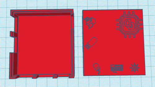
After I was satisfied with the design, I exported it as an STL file, sliced it based on printer settings, and finally printed it. The STL file is also available for download from Thingiverse, and you can print your own casing using it.
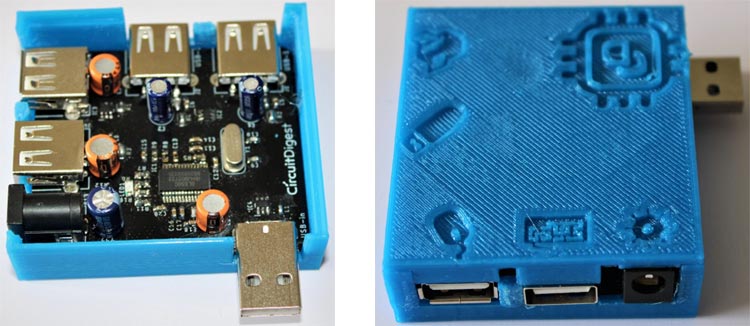
After the print was done, I proceeded with assembling the project set-up in a permanent enclosure for future use, and everything was nicely fit as you can see below:
Testing and Validating Your USB Hub Circuit
Proper testing ensures your USB hub circuit operates reliably before deployment. After assembling the PCB and fixing the PCB inside a 3-D printed enclosure, I plugged this into one of my Laptop’s USB ports and then connected 4 USB devices to its USB ports. All four devices connected to this USB Hub were working seamlessly.
USB Functionality Testing
| Test | Procedure | Expected Result |
| Enumeration | Connect hub to Windows/Linux/Mac computer | OS recognizes "USB 2.0 Hub" in Device Manager |
| Port Detection | Connect USB flash drive to each port sequentially | All four ports detect devices correctly |
| Data Transfer | Copy 1GB file to USB drive through hub | Transfer completes without errors, speed >30 MB/s |
| Power Delivery | Connect high-power USB device (500mA) | Device operates normally, no brownout |
| Multiple Devices | Connect four devices simultaneously | All devices enumerate and function correctly |
| Hot-Plug Test | Repeatedly connect/disconnect devices | No enumeration failures, instant recognition |
| External Power | Plug in 5V adapter, connect power-hungry device | Device receives adequate power, hub reports self-powered |
Frequently Asked Questions (FAQs) About DIY USB Hubs
⇥ Q1: What is the distinction between a self-powered USB hub and a bus-powered USB hub?
The bus-powered USB hub gets all of its power from the host USB port (up to a total of 500mA) while the self-powered hub gets its power from a 5V external power adapter (up to 500mA per port or 2A total). The benefit of being self-powered is that it can power devices that draw high amounts of current, like external hard drives and multiple phones.
⇥ Q2: Is there an IC that can replace the GL850G USB 2.0 hub IC?
Yes, ICs such as FE1.1s, TUSB4041I, USB2514, and USB2422 can be used in place of the GL850G USB 2.0 hub IC. All will have their specific features and pin-outs to keep in mind; however, take note that the GL850G is a popular choice since it doesn't require many external parts, it's widely available, and has been reliable from a commercial perspective. Check datasheets to see if you're within the required tolerances of the IC specs to replace your original IC.
⇥ Q3: Why are differential pairs' routing parameters important during the design of the USB hub board?
USB 2.0 Hi-Speed mode can transmit data at 480 Mbps using differential signalling. Use of matched-length, 90Ω pairs avoids signal reflection, reduces electromagnetic interference, and ensures reliable data transfer. Mismatched impedance can result in eye closure and enumeration failure. Routing of differential pairs is vitally important to maintain USB compliance.
⇥ Q4: What will happen if I do not include ESD protection on my homemade USB hub?
Without transil TVS diodes, static electricity occurrences generated during hot-plugging devices into the USB hub, can cause irreversible damage to the hub controller IC or corruption to the data line. ESD voltages can even reach upwards to 15kV from human contact. Protection of the IC is provided when the TVS diodes limits these voltage spikes to a safe level (<5V) to ensure everyday use of the sensitive CMOS circuitry. Any professional hub board always has ESD protection built in.
⇥ Q5: What's the maximum current for each port in a powered USB hub you will be building yourself?
For a USB 2.0 powered hub, you are limited to a maximum of 500mA per port. If the powered hub connects to a computer, the 500mA is split across the power of all of the ports on the hub. This means that if you connect a powered hub that has four ports to a computer, you could only get a collective total of 500mA from all four ports. However, if the hub comes with it's own external power source (minimum of 2A) and isn't powered through the computer, it could then give you 500mA to each port simultaneously. The hub will have PTC fuses and overcurrent protection to protect you from any power issues.
⇥ Q6: Why do I use a 12MHz crystal for the USB hub circuit?
The GL850G USB hub controller requires a specific clock reference for USB timing. Since USB timing needs to be precise, a 12MHz fundamental-mode crystal oscillator provides this timing reference with the accuracy of ± 100 ppm that the USB specification calls for. The IC provides an internal multiply using phase-locked loops that will provide a 48MHz (USB Full-Speed) and 480MHz (USB Hi-Speed) clock reference.
⇥ Q7: Can I use a similar method to build a USB 3.0 hub?
No, because the USB 3.0 (SuperSpeed, 5 Gbps) will require a significantly more complex PCB with multiple differential pairs (TX+/TX-, RX+/RX-) and impedance control of 85 Ω to 95 Ω pairs, and it requires at minimum a 4-layer PCB. Another point would be that USB 3.0 hub ICs like the VL812 or GL3523 will require even more components since USB 3.0 is considerably more complex, proper EMI management and shielding is also a large consideration. So I would recommend for hobbyists and DIY or making it themselves to stick with USB 2.0.
Conclusion: Build Your Own Professional USB Hub
In this comprehensive guide, you learned how to develop, engineer, and test a professional-grade 4-port USB hub circuit board using the GL850G USB 2.0 hub IC. By adhering to best PCB design practices, including differential pair routing, protection circuits with ESD protection, and accommodating bus-powered or self-powered operating modes, you can successfully build a quality DIY USB hub and power supply similar to a commercial (store-bought) product.
Key takeaways from this project:
∗ Basics of USB 2.0 protocol and hub architecture.
∗ Appropriate USB hub schematic design with overcurrent and ESD protection.
∗ Important PCB layout techniques for high-speed differential signalling.
∗ Professional assembly and testing practices.
∗ Design a custom enclosure for your finished product.
Whether you will need extra ports on your workstation, are interested in understanding USB technology, or want to integrate a hub into another project, this USB hub circuit diagram is a good starting point.
The complete work for this project can be found in the video below. If you have any questions, you can leave them in the comment section below, or you can also use our forum.
Innovative Projects Using USB Technology
Discover innovative USB electronics projects designed to help you learn and build practical USB-powered and USB-interface devices. These projects cover topics like USB communication with microcontrollers, data transfer circuits, custom USB gadgets, and power management applications—perfect for hobbyists and embedded system enthusiasts.

How to Boot Raspberry Pi from USB without SD Card
Want to boot your Raspberry Pi from USB instead of unreliable SD cards? If you've used a Raspberry Pi long enough, you've probably faced the dreaded SD card failure. So if you're wondering whether your Pi can ditch the microSD and run from USB alone, this guide is for you.

Finally, we will publish sensor data to the Azure IoT server using the MQTT protocol. In this tutorial, we will learn how to set up and configure an Azure server and send data using a Raspberry Pi.

How to use USB Audio Device and Microphone with Raspberry Pi Zero W
This tutorial is the part of our Raspberry Pi Zero series where we are going to install USB sound card in Raspberry Pi zero W and we will use ALSA utilities to test sound card and sound device.
Comments
Great project. Where are the fieles to download please?? Thank you
Design and BOM need more details....
What are the ohm values for the ferrite beads used in this project? The same question for the thermistors used Can you provide more detail about the crystal used such as pf value.
Can you please provide more detail as to how to find the exact thermistors needed for this project please?

Are you releasing the Gerber files for this project?
If I have missed them in the article can you identify where I can find them.
Thanks
Ray Drury