As many of us know an Integrated Circuit or IC is a combination of many small circuits in a small package which together performs a task. Like an Operational Amplifier or 555 Timer IC is built by a combination of many Transistors, Flip-Flops, Logic Gates and other combinational digital circuits. Similarly a Flip-Flop can be built by using a combination of Logic Gates and the Logic Gates itself can be built by using a few Transistors. Learning how to make an OR gate using transistor is fundamental to understanding digital electronics. An Integrated Circuit (IC) combines multiple small circuits to perform complex tasks.This guide demonstrates OR gate using transistor circuit design, explaining both simple and improved implementations using NPN transistors.
Logic Gates are the basics of many digital electronic circuits. From the basic Flip-Flops to Microcontrollers Logic gates form the underlying principle on how bits are stored and processed. They state the relation between every input and output of a system using an Arithmetic logic. There are many different types of logic gates and each of them has a different logic which be used for different purposes. But the focus of this article will be on the OR Gate because later we would be building an OR Gate using a BJT transistor circuit, similar to the AND Gate transistor circuit that we built earlier.
Table of Contents
What is an OR Logic Gate?
OR gates implement Boolean ‘disjunction’, that is it helps in finding the maximum of the given binary inputs. Understanding OR gate using transistor in logic gates begins with Boolean disjunction logic. The logic operation is straightforward: the output is HIGH (1) when at least one input is HIGH. If either input A or input B (or both) is HIGH, the output becomes HIGH.

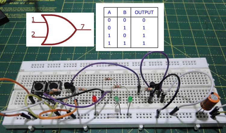
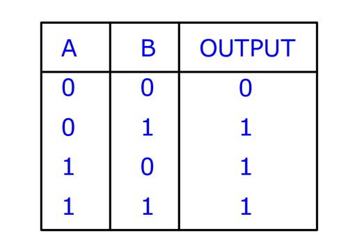
OR gates have the circuit symbol show in figure 1, the curved end is the input and the pointy end is the output. The logic they follow is simple, the output is true if any one input is true or if either input A or input B is true. The OR Gate Truth Table is shown below.
OR Gate Truth Table
This principle can be extended to as many inputs as is needed, the output is true if any one (or at least one) of the inputs is true. In this article we will be building an OR Logic gate using transistor, if you want to know more on OR gate and how they work you can check this basics of OR gate article.
Components Required for OR Gate Using Transistor
To build an OR gate using transistor circuit, you'll need these readily available components:
- NPN small signal transistors (2N2222, BC547, etc.)
- 1K resistors
- 10K resistors
OR Gate Using Transistor Circuit Diagram
The first version of the OR gate is the simplest one – it consists of two paralleled emitter followers sharing a common emitter resistor.The simplest OR gate using transistor circuit diagram consists of two parallel-connected emitter followers sharing a common emitter resistor.
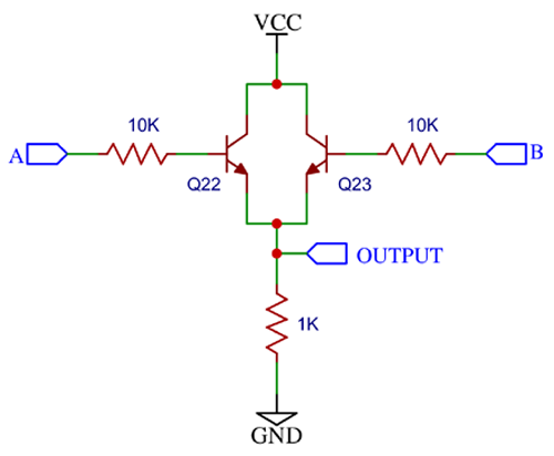
The above circuit diagram shows the simplest way to build an OR gate using NPN transistors. When input A is held high, a small current passes through the base of transistor Q22. This turns Q22 on, and (relatively) large current flows from the collector to the emitter. The current is dropped across the emitter resistor. The voltage across the emitter resistor is VCC – 0.7V, so the output ‘follows’ the input with a gain of a little less than unity. The same thing happens when input B is held high. When both the inputs are held high, both transistors are active, but the same voltage is dropped across the emitter resistor, and the output is still high. This circuit shows perfect OR behaviour. Connecting switches and LEDs to the input shows the behaviour of the circuit better as you can see in the below images.
This OR gate using NPN transistor design features two transistors (Q1 and Q2) with their emitters connected to a common load resistor. The key design elements include:
∗ Input Configuration: Two independent base inputs (A and B) and current limiting resistors.
∗ Transistor Configuration: This is a parallel configuration so that either transistor can drive the output HIGH.
∗ Output Stage: The common emitter resistor creates a voltage divider that the output signal is measured across.
∗ Voltage Levels: The output voltage is VCC - 0.7V when either transistor is turned on (this accounts for the base-emitter junction drop).
How OR Gate Using Transistor Works - Operating Principle
⇒ Case 1: When both the inputs are low, the output is low
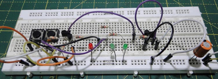
⇒ Case 2: When one input is low and the other is high, the output is high
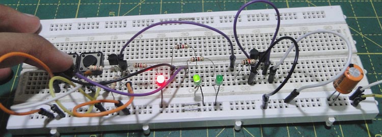
⇒ Case 3: And vice versa, when other input is low, the output is high
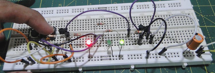
⇒ Case 4: And finally when both inputs are high, the output is high
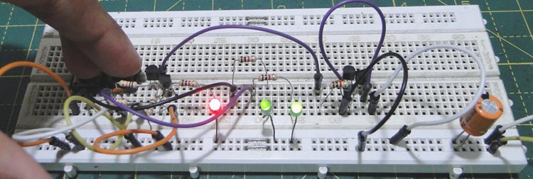
As you can see the circuit is working and following the truth table we discussed earlier. You can stop here if you are happy with this crude circuit, but if you want to make some improvements to the circuit read on.
Improved OR Gate Using Transistor Circuit
While the basic OR gate transistor circuit demonstrates fundamental logic operation, professional IC design requires optimization for speed, power efficiency, and drive capability.
The circuit shown above was a very simple implementation of the OR gate, but this circuit is seldom used in the manufacture of ICs, for a few reasons. If we connect one input to VCC, a switch to the other input and probe the input and the switch and trigger on the rising edge of the switch, we notice a small problem.
Optimization Techniques
The output goes high only after some time, i.e. does not respond instantly to the input. The time taken for the input to be seen at the output is called propagation delay. The same thing happens when the input is removed. The output takes some time to go back to ground.
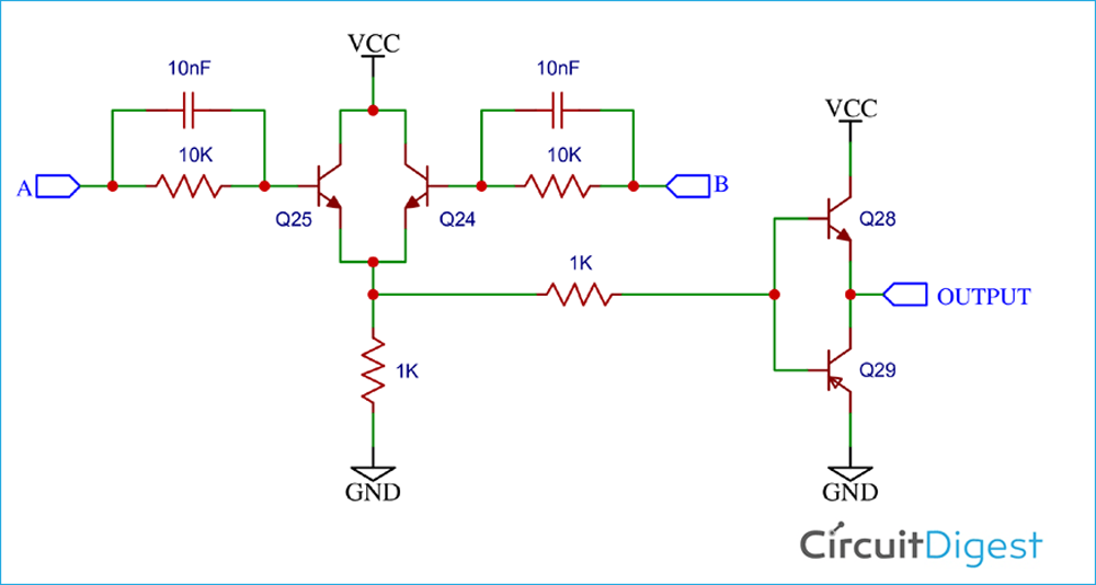
This happens because of the transistor’s base capacitance. One solution would be to decrease the values of all the resistors, so that more current flows and the capacitances are charged quickly. But this would result in too much power dissipation. To circumvent this, we add two small (<10nF) ‘speedup’ capacitors across the base resistor to reduce the ‘storage’ time.
Another problem is that this circuit cannot sink as much current as it sources. Sourcing is not a problem because there’s at least one transistor turned on (when at least one input is high) that is connected directly to the output, so that the output can provide a decent amount of current.
However, when the transistor is turned off, only the 1K resistor pulls the output down, and sink current is limited. To make the drive symmetrical, an output push-pull stage is added. Both these modifications greatly reduce rising and falling propagation delays.
Real-World Applications of OR Gates
Along with the AND gate, the OR gate forms an integral part of all logic circuits. For example, if there are ten inputs that a microcontroller needs to monitor, a 10 input OR gate will tell the controller if any one of the inputs is high without needing ten input pins.
Another interesting applications of logical OR is in your car. The seatbelt warning light turns off only when all the doors are closed, in other words, if any one (or at least one) of the doors are open, the alarm lights up. Understanding these applications clarifies why mastering how to make OR gate using transistor remains relevant.
- Input Multiplexing: If a microcontroller is tasked with monitoring ten sensors but has limited input pins, a 10-input OR gate can signal the status of the ten sensors. If any of the ten sensors detects an event, the 10-input OR gate will signal the microcontroller with a single input pin instead of utilizing ten input pins.
- Automotive Safety Systems: The car door ajar warning is a dynamic example of OR logic; if one or more doors are ajar, the warning light engages. Seatbelt reminders use similar OR gates to evaluate multiple seats.
- Interrupt controllers: Computer systems use OR gates to combine several interrupt sources into a single line fed to the processor consolidating many interrupt lines into a single interrupted alert from the hardware.
- Alarm systems: Home security systems use OR gates to trigger alarms when any sensor detects an intrusion (a noise detector, door sensor, or window sensor).
- Power management: OR gates, combined with AND gates, simply create complex power sequencing logic in electronics to ensure components function in an orderly fashion.
- Boolean expression implementation: OR gates can implement any Boolean function, in conjunction with AND and NOT gates, via the language of Boolean logic called the Sum of Products (SOP) expressions; these gates are the building blocks for nearly all programmable logic devices.
Frequently Asked Questions on OR Gate Using Transistor
⇥ 1. What does adding speedup capacitors accomplish in high-speed applications with OR gates?
Speedup capacitors (typically 4.7-10nF) can reduce propagation delay caused by the capacitor component at the base of a transistor. When switching occurs, speedup capacitors create a burst of current that assists in rapidly charging, or discharging, the base-emitter junction during the turn-on or turn-off intervals, resulting in a decrease in effective storage time without permanent power consumption. This result is a critical component of high-speed digital systems.
⇥ 2. What is the main difference between OR gate transistor circuits and AND gate transistor circuits?
OR gates are implemented with transistors in parallel, and thus only one of the active transistors is needed to produce a HIGH output. AND gates are implemented with transistors in series, and thus all active transistors are needed to produce a HIGH output. Thus, OR gates can be expressed as a disjunction (A+B), and AND gates through a conjunction (A·B), in the language of standard Boolean algebra terminology.
⇥ 3. How many inputs can a transistor OR gate have?
Theoretically unbounded, but real designs usually constrain inputs to 8-12 because of fan-in limitations. Each input adds circuit complexity, power, and propagation delay. The common emitter resistor must conduct aggregate current of all active transistors. Cascade several small OR gates for improved performance for more inputs.
⇥ 4. What are the sources of the propagation delay for an OR gate, in terms of the transistors themselves?
Propagation delay in OR gates is seen, or the result of, exposing the time it takes for positivity charge carriers to charge and discharge the capacitance in the base or other junction capacitances, including turning the transistor ON or OFF, and then possibly negative charge carrier biasing during the turn OFF process. The delays of these processes may be, depending on the specific performance characteristics of the transistor component, the value of the resistors, and the location, similar observations, are on the order of 50 to 500 nanoseconds.
⇥ 5. Can we directly drive LEDs and relays with OR gate circuits?
Simple OR gates can drive LEDs (10-20mA) directly, using current-limiting resistors. Relays, on the other hand, require more current (50-500mA) so you need to include a buffer transistor after the OR gate output for more drive capability. OR gate use the improved circuit, which has a push-pull output stage, and can drive loads directly (50-100mA).
⇥ 6. How can I test if the OR gate circuit is functioning correctly?
Employ a multimeter or LED to check all four states of the truth table: measure output voltage for inputs 00, 01, 10, and 11. Proper operation indicates LOW output (close to 0V) only for both LOW inputs and HIGH output (close to VCC) for any other input combination. Oscilloscope testing indicates propagation delays and switching behavior.
⇥ 7. What voltage levels represent HIGH and LOW for transistor OR gates?
For 5V logic, HIGH is typically 3.5-5V, while LOW is typically 0-0.8V. There is a range from 0.8-2.0V that is not defined in order to prevent unwanted triggering. Output HIGH is VCC minus the saturation voltage of the transistor (approximately 0.7V). Input HIGH is typically greater than the base-emitter threshold (0.6-0.7V) plus enough base current to saturate the transistor.
Exploring Basic Logic Gates: From Transistor-Level Design to VHDL Implementation
Learn how basic logic gates like NOT and NAND work by designing them with transistors and simulating their behavior using VHDL in ModelSim for a complete understanding of digital logic. If you want to know more about those topics, links are given below.
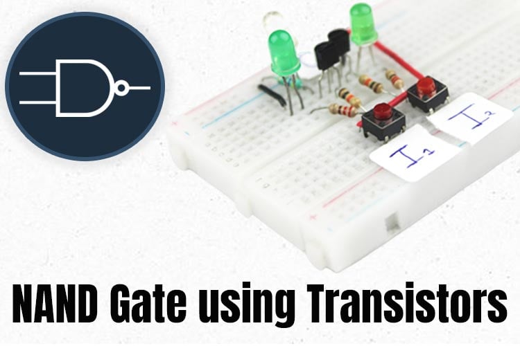
How to Build a NAND Gate with Transistors?
In the realm of digital electronics and logic circuits, the NAND gates stands as a fundamental cornerstone that wields immense power in information processing. NAND, short for Negated AND, is a logical operation that produces an output of low only when all of its inputs are high.
Implementation of Basic Logic Gates using VHDL in ModelSim
This tutorial is all about designing the basic logic gates using different VHDL modeling and their corresponding simulations. If you haven’t installed the ModelSim software, please refer to the previous tutorial “Getting Started with VLSI and VHDL using ModelSim -A Beginner's Guide” for installation guidance.
Designing NOT Gate using Transistors
We have already built an AND Gate using Transistor and an OR Gate using Transistor following that in this article we will build NOT gate using BJT Transistor. Before we begin let's understand the basics of NOT gate and transistors with their working.



why use a PNP for the second set another NPN wouldn't it have worked?